

Linear Technology LTC1531 Datasheet
FEATURES
■
UL Recognized File E151738 to UL1577
■
Self-Powered Across Isolation Barrier
■
2500V
■
2.5V Isolated Reference, I
■
Zero-Cross Output for Line Power
■
Dual Differential Input Comparator
■
High Input Impedance Comparator
Isolation
RMS
LOAD
= 5mA
U
APPLICATIO S
MAX
LTC1531
Self-Powered Isolated
Comparator
U
DESCRIPTIO
The LTC®1531 is an isolated self-powered dual differential
comparator. An internal capacitive isolation barrier provides 2500V
its output. The part provides UL-rated isolated comparisons without the need for an isolated supply since both
comparator power and output data are transmitted across
the capacitive barrier. The comparator data is transferred
differentially across the isolation barrier to provide high
common mode voltage and noise immunity.
of isolation between the comparator and
RMS
■
Self-Powered Isolated Sensing
■
Isolated Temperature Control
■
Isolated Voltage Monitor
■
Isolated Switch Control
, LTC and LT are registered trademarks of Linear Technology Corporation.
U
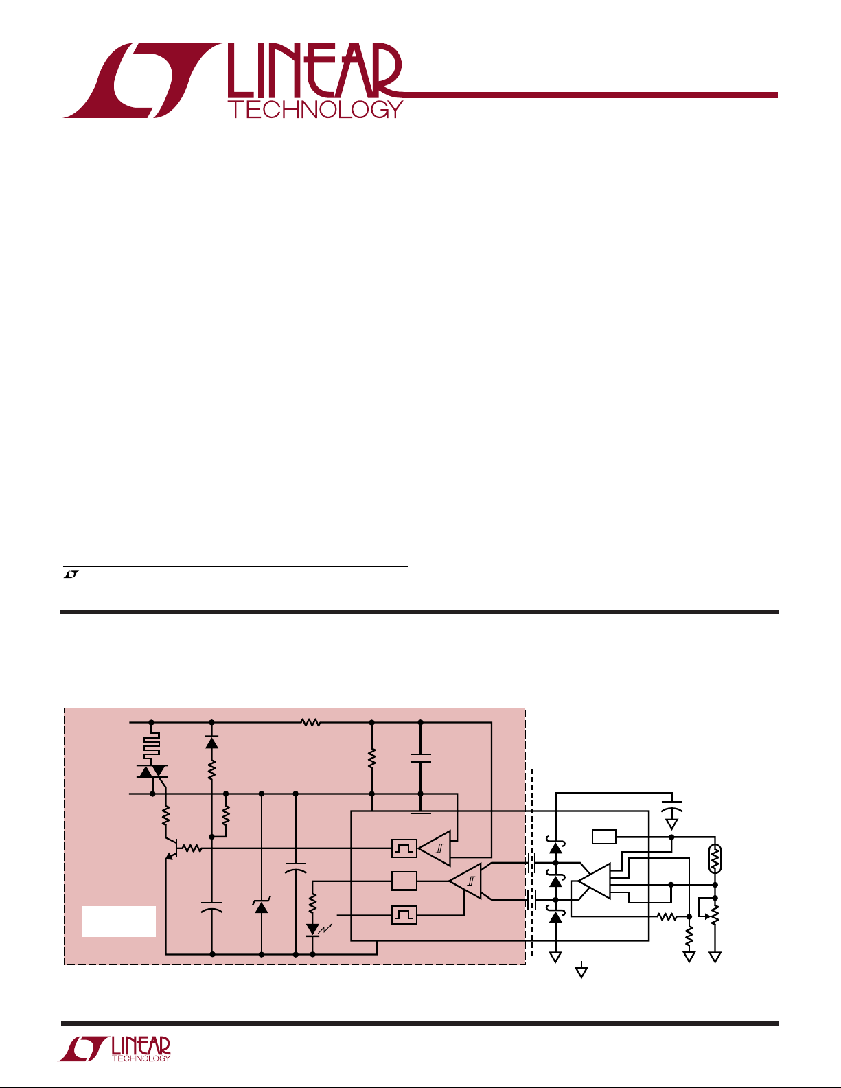
TYPICAL APPLICATION
Isolated Thermistor Temperature Controller
AC
120V
TECCOR
Q4008L4
OR EQUIVALENT
NEUTRAL
DANGER!
LETHAL VOLTAGES
IN THIS SECTION!
2N2222
LOAD
25Ω
150Ω
1k
–5.6V
1N4004
3k
3W
750Ω
0.5W
+
20µF
50V
5.6V
R1
680k
+
100µF
390Ω
LED
V
CC
ZCDATA
DATA
VALID
GND
R2
47k
The isolated side can supply a 2.5V reference output to
power external sensor circuits such as a thermistor bridge.
The dual differential comparator inputs allow for comparison of two differential voltages as well as single-ended
voltages. The powered side provides a latched data output
as well as a pulsed zero-cross comparator output for
controlling a triac. The part is available in a 28-lead SO
package.
C1
SHDN
QD
0.01µF
ZCPOS
LTC1531
ZCNEG
ISOLATION
BARRIER
V
PW
ISOGND
1
*HYSTERESIS = 1°C AT T
V
REG
2.5V
V1
V2
+
V3
–
V4
CMPOUT
R5*1M
= ISOLATED GROUND
1
R
+
R
1µF
B = 3807
T
1
O
T
R6
22k
1
O
=
THERM
B (1/T – 1/TO)
O • e
= 297°K
THERM
30k
YSI 44008
R4
50k
1
1531 TA01
1

LTC1531
WW
W
U
ABSOLUTE MAXIMUM RATINGS
(Note 1)
Total Supply Voltage (VCC to GND) ............................ 7V
Input Voltages
Isolated Comparator
(V1 to V4).............................. –0.3V to (VPW + 0.3V)
SHDN, ZCPOS, ZCNEG ......................... –0.3V to 12V
Current
Input Pins .......................................................±10mA
ZCDATA, VALID, DATA .................................. ±10mA
Operating Temperature Range ..................... 0°C to 70°C
Storage Temperature Range ................. –65°C to 150°C
Lead Temperature (Soldering, 10 sec)..................300°C
U
W
PACKAGE/ORDER INFORMATION
TOP VIEW
V
1
CC
SHDN
2
ZCNEG
3
ZCPOS
4
11
V
PW
CMPOUT
Consult factory for Industrial and Military grade parts.
12
13
V
REG
14
ISOGND
28-LEAD PLASTIC SO (ISO)
T
= 125°C, θJA = 125°C/W
JMAX
SW PACKAGE
28
27
26
25
18
17
16
15
GND
ZCDATA
DATA
VALID
V1
V2
V3
V4
ORDER PART
NUMBER
LTC1531CSW
U
ELECTRICAL CHARACTERISTICS
The ● denotes specifications which apply over the full operating temperature range, otherwise specifications are TA = 25°C, VCC = 5V.
SYMBOL PARAMETER CONDITIONS MIN TYP MAX UNITS
I
VCC
V
ZCOS
V
HYS
f
SAMPLE
V
OS
R
VIN
I
VIN
V
REG
R
VREG
I
CMPOUT
t
VREG
V
PWH
I
VPW
V
ISO
Supply Current SHDN = VCC, No Load ● 10 14 mA
SHDN = 0V
Zero-Cross Offset VCM = V
Zero-Cross Hysteresis VCM = VCC (Note 7) ● 200 800 mV
Isolated Comparator Sample Rate V
Isolated Comparator Offset V1 = V2, V3 = V4 ● 2.0 4.0 mV
Isolated Comparator V1 = V3 = 2.5V, V2 = V4 = 0V 18 MΩ
Input Impedance V1 = V2 = 1.25V, V3 = V4 = 0V 300 MΩ
Isolated Comparator Input Current V1 = V3 – 2.5V, V2 = V4 = 0V ±1nA
V
REG
V
Output Impedance 2mA to 5mA Load ● 415 Ω
REG
CMPOUT High Impedance Leakage Current V
V
On-Time ● 90 108 130 µs
REG
VPW, Power Detect Enable Voltage 3.3 V
Current Transfer to V
Isolation Voltage 1 Minute (Note 6) ● 2500 V
PW
CC
Not Loaded (Note 2) 300 Hz
REG
V1 – V3 = 2V, V4 – V2 = 2V
f
= 700Hz (Note 4)
SAMPLE
2mA Load VPW = 3.3V (Note 5) ● 2.40 2.50 2.55 V
= 2.5V 1 nA
CMPOUT
VPW = 0V 45 µA
V
= 3.3V 30 µA
PW
1 Second ● 4500 V
● 0.2 10 µA
● ±30 ±120 mV
● 2.0 4.0 mV
RMS
DC
2
LTC1531
ELECTRICAL CHARACTERISTICS
The ● denotes specifications which apply over the full operating temperature range, otherwise specifications are TA = 25°C, VCC = 5V.
SYMBOL PARAMETER CONDITIONS MIN TYP MAX UNITS
V
IH
V
IL
V
OH
V
OL
I
, I
INL
INH
dV/dt Continuous dV/dt Rejection (Note 8) ● 50 70 V/µs
C
ISO
SHDN Input High Voltage VCC = 4.5V ● 2.4 V
SHDN Input Low Voltage VCC = 5.5V ● 0.8 V
DATA, VALID, ZCDATA Output High Voltage VCC = 4.5V, IO = –400µA ● 3.0 4.3 V
DATA, VALID, ZCDATA Output Low Voltage VCC = 4.5V, IO = 1.6mA ● 0.2 0.4 V
SHDN Low or High Level Input Current VIN = 5V, 0V ● ±1 µA
2pF
Note 1: Absolute Maximum Ratings are those values beyond which the life
of a device may be impaired.
Note 2: The sample rate is not continuous, but depends on V
charging
PW
rate. See Applications Information.
Note 3: See Applications Information for further description of the
comparator switched-capacitor input circuit.
Note 4: The sample rate, f
Note 5: Load on CMPOUT pulls current from V
Note 6: Value derived from 1 second test.
Note 7: Zero-cross hysteresis is the minimum amount of signal amplitude
above or below 0V differential to retrigger the zero-cross comparator.
Note 8: Parameter not tested but guaranteed by design.
UW
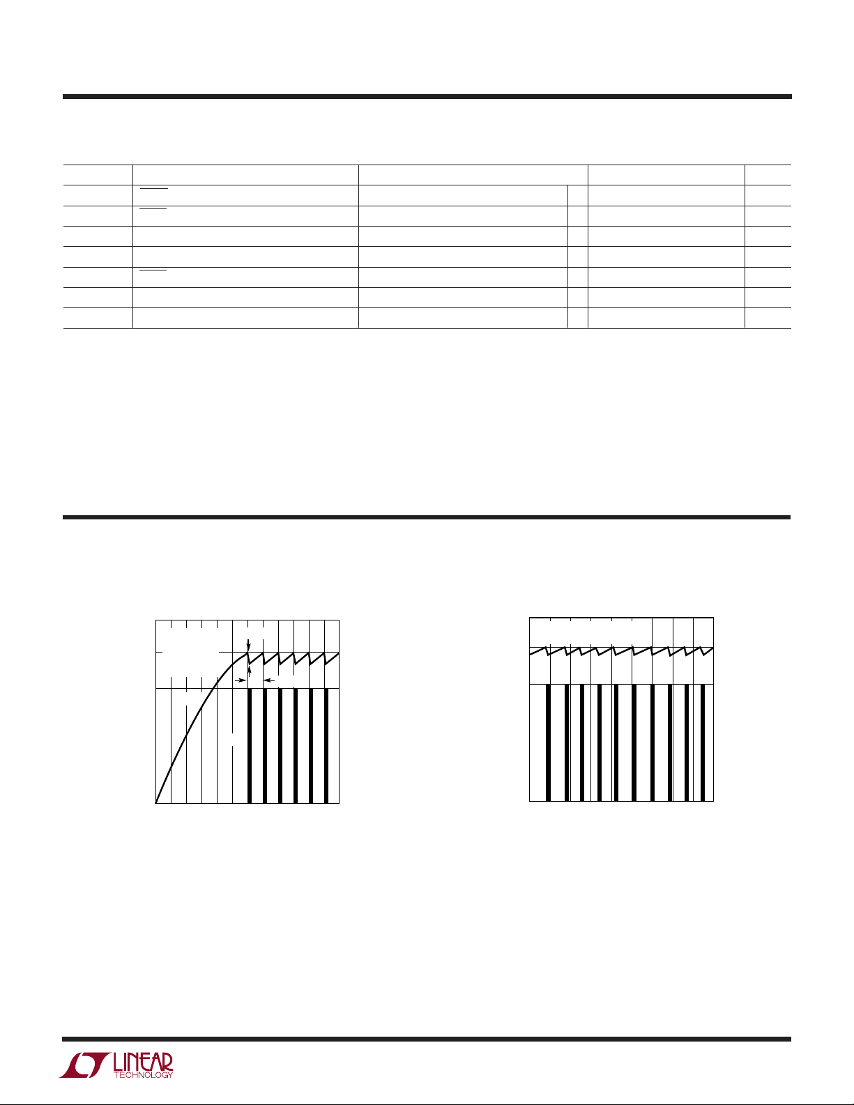
TYPICAL PERFORMANCE CHARACTERISTICS
V
RIPPLE
t
SAMPLE
V
REG
(V)
PW
V
3.3
2.5
VCC = 5V
= 1µF
C
VPW
= 5mA
I
VREG
= 25°C
T
A
V
PW
(V)
REG
V
3.3
2.5
SAMPLE
VCC = 5V, C
I
VREG
VPW
= 100µA, TA = 25°C
, varies with loading on VPW and V
when CMPOUT is high.
REG
= 1µF
REG
.
0
NOTES: V
t
RIPPLE
SAMPLE
100
TIME (ms)
DEPENDS ON C
DEPENDS ON I
Figure 1. VPW Power-Up and
V
Samples vs Time
REG
200 300
AND I
VPW
VPW
+ I
VREG
VPW
+ I
VREG
1531 F01
0
0
NOTE: NONPERIODIC SAMPLES DUE TO DEPENDENCE
ON V
SAMPLING
PW
Figure 2. V
(I
VREG
2010
TIME (ms)
> 3.3V AND THE POWER-LISTEN CYCLE
REG
30 40
1531 F02
and VPW vs Time
= 100µA)
3
LTC1531
UW
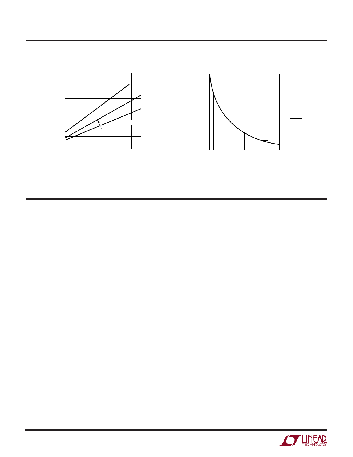
TYPICAL PERFORMANCE CHARACTERISTICS
30
TA = 25°C
25
20
(ms)
15
SAMPLE
t
10
5
0
0
Figure 3. Average t
VCC = 4.5V
VCC = 5.5V
VCC = 5V
I
VREG
2
(mA)
SAMPLE
1
3
vs I
4
1531 F03
VREG
UUU
PIN FUNCTIONS
VCC (Pin 1): Powered Side Power Supply.
SHDN (Pin 2): Active Low Chip Shutdown. A low signal
causes the circuitry to power down. DATA logic output
level will be reset to zero during power-down.
ZCNEG (Pin 3): Zero-Cross Comparator Negative Input.
ZCPOS (Pin 4): Zero-Cross Comparator Positive Input.
VPW (Pin 11): Isolated Power Supply. Connect to an
external storage capacitor.
4500V
BREAKDOWN
LIMIT
RMS
V
10k 10M
100k 1M 100M
FREQUENCY (Hz)
Figure 4. V
2500V
450V
45V
vs Frequency
RMS
RMS
SLEW RATE = (π)(f)(V
= (1.11)(f)(V
50V/µs
(1.11)(f)
4.5V
450mV
1531 F04
= V
RMS
P-P
)
RMS)
equal to (V1 + V2)/2 > (V3 + V4)/2 or equivalently (V1 – V3)
> (V4 – V2).
V3 (Pin 16): Comparator Negative Input.
V2 (Pin 17): Comparator Positive Input.
V1 (Pin 18): Comparator Positive Input.
VALID (Pin 25): Pulsed Output. Indicates when valid data
was received from the comparator. May be used to clock
DATA to external circuitry.
CMPOUT (Pin 12): Isolated Latched Comparator Data.
CMPOUT is active when V
is on. The CMPOUT output
REG
can be used on the isolated side for hysteresis (see
applications). The output will contain the result of the
previous comparison. When V
is low, the CMPOUT pin
REG
is Hi-Z.
V
(Pin 13): Isolated 2.5V Regulated Output. Pulsed on
REG
for 100µs with a maximum load current of 5mA. V
REG
also
supplies power to the CMPOUT output (Pin 12).
ISOGND (Pin 14): Isolated Side Power Ground.
V4 (Pin 15): Comparator Negative Input. The comparator
inputs are summed together with the comparison output
4
DATA (Pin 26): Latched Comparator Result. DATA holds
the value of the last valid comparison result. DATA changes
only when a valid comparison was received from the
isolated side.
ZCDATA (Pin 27): A 24µs to 30µs Pulsed Output. The
pulse occurs when the DATA output is high and the zerocross comparator inputs (ZCPLS-ZCNEG) cross zero volts
differential. Typically the zero-cross input signal is an RC
phase shifted AC sine wave. This output is a TTL level pulse
that can be used for firing an external triac.
GND (Pin 28): Power Supply Low Impedance Ground
Connection.
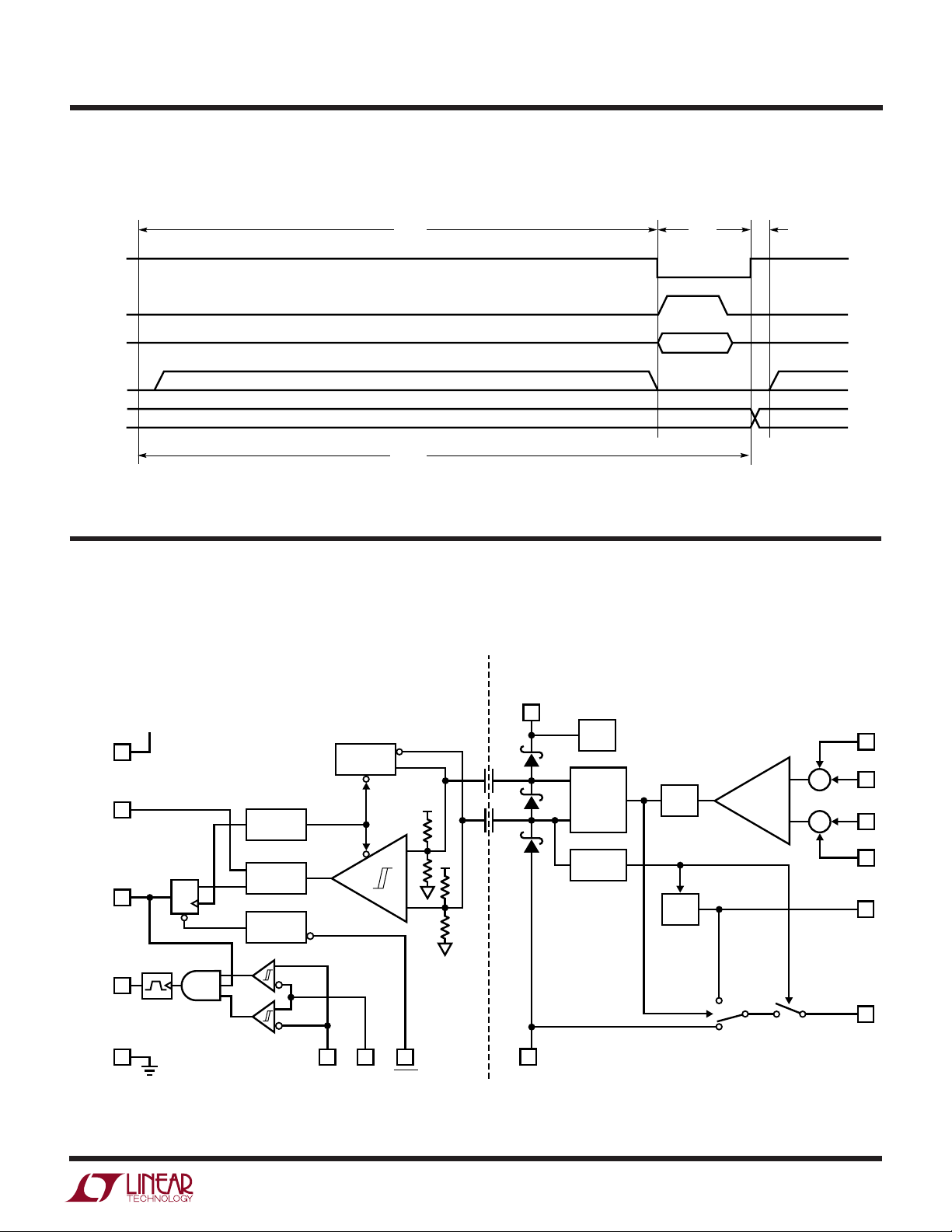
UWW
TI I G DIAGRA
LTC1531
V
REG
CMPOUT
VALID
DATA
BLOCK DIAGRAM
W
POWER CYCLE
960µs
POWER
Hi-Z
POWER-LISTEN CYCLE
1152µs
ISOLATION
BARRIER
LISTEN CYCLE
192µs
LISTEN
108µs
200ns
1531 TD01
V
VALID
DATA
ZCDATA
GND
POWERED SIDE
V
CC
1
CC
25
TIMING
VOLTAGE
PUMP
V
PW
11
3.3V
DET
TRANSMIT
AND
DRIVER
+
Q
26
27
28
D
R
ZERO-CROSS
COMPARATOR
DECODE
POWER-ON
RESET
–
4
ZCPOS ZCNEG SHDN
2
3
14
ISOGND
TIMING
ISOLATED SIDE
LATCH
2.5V
REG
COMPARE
V1
18
V2
+
–
17
Σ
V3
16
Σ
V4
15
V
REG
13
CMPOUT
12
1531 BD
5
 Loading...