

Linear Technology LTC1530 Datasheet
FEATURES
■
High Power Buck Converter from 5V or 3.3V
Main Power
■
Adjustable Current Limit in S0-8 with
Topside FET R
■
No External Sense Resistor Required
■
Hiccup Mode Current Limit Protection
■
Adjustable, Fixed 1.9V, 2.5V, 2.8V and 3.3V Output
■
All N-Channel MOSFET Synchronous Driver
■
Excellent Output Regulation: ±2% over Line, Load
DS(ON)
Sensing
and Temperature Variations
■
High Efficiency: Over 95% Possible
■
Fast Transient Response
■
Fixed 300kHz Frequency Operation
■
Internal Soft-Start Circuit
■
Quiescent Current: 1mA, 45µA in Shutdown
U
APPLICATIO S
LTC1530
High Power Synchronous
Switching Regulator Controller
U
DESCRIPTIO
The LTC®1530 is a high power synchronous switching
regulator controller optimized for 5V to 1.3V-3.5V output
applications. Its synchronous switching architecture drives
two external N-channel MOSFET devices to provide high
efficiency. The LTC1530 contains a precision trimmed
reference and feedback system that provides worst-case
output voltage regulation of ±2% over temperature, load
current and line voltage shifts. Current limit circuitry
senses the output current through the on-resistance of
the topside N-channel MOSFET, providing an adjustable
current limit without requiring an external low value sense
resistor.
The LTC1530 includes a fixed frequency PWM oscillator
that free runs at 300kHz, providing greater than 90%
efficiency in converter designs from 1A to 20A of output
current. Shutdown mode drops the LTC1530 supply current to 45µA.
■
Power Supply for Pentium® II, AMD-K6®-2, SPARC,
ALPHA and PA-RISC Microprocessors
■
High Power 5V to 1.3V-3.5V Regulators
U
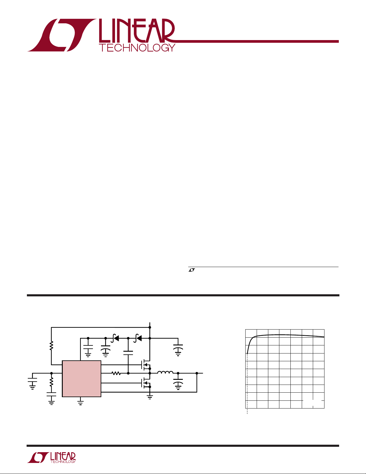
TYPICAL APPLICATIO
V
IN
5V
MBR0530T1 MBR0530T1
0.1µF
+
10µF
G1
I
G2
V
OUT
†
COILTRONICS CTX02-13198
OR PANASONIC ETQP6F2R5HA
††
AVX TPSE337M006R0100
20Ω
FB
0.22µF
Q1*
Q2*
COILTRONICS (561) 241-7876
C1
150pF
0.022µF
2.7k
PV
I
CC
MAX
COMP
R
LTC1530-3.3
C
10k
C
C
GND
Figure 1. Single 5V to 3.3V Supply
The LTC1530 is specified for commercial and industrial
temperature ranges and is available in the S0-8 package.
, LTC and LT are registered trademarks of Linear Technology Corporation.
Pentium is a registered trademark of Intel Corp.
AMD-K6 is a registered trademark of Advanced Micro Devices, Inc.
+
C
**
IN
1200µF
× 4
†
L
O
2µH
††
+
C
O
330µF
× 7
* SILICONIX SUD50N03-10
** SANYO 10MV1200GX
V
3.3V
14A
1530 F01a
OUT
Efficiency vs Load Current
100
90
80
70
60
50
40
EFFICIENCY (%)
30
20
10
0
0
2
0.3
4
LOAD CURRENT (A)
8
6
TA = 25°C
10
12
14
1530 F01b
1
LTC1530
TOP VIEW
G1
G2
I
FB
I
MAX
PV
CC
GND
S8 PACKAGE
8-LEAD PLASTIC SO
1
2
3
4
8
7
6
5
*V
SENSE
/
V
OUT
COMP
WWWU
ABSOLUTE AXI U RATI GS
(Note 1)
Supply Voltage
PVCC........................................................................ 14V
Input Voltage
IFB (Note 2) ............................................... PVCC + 0.3V
I
........................................................ –0.3V to 14V
MAX
IFB Input Current (Notes 2,3) ............................–100mA
Operating Ambient Temperature Range
LTC1530C ............................................... 0°C to 70°C
LTC1530I............................................ –40°C to 85°C
Maximum Junction Temperature
LTC1530C, LTC1530I ...................................... 125°C
Storage Temperature Range ................. –65°C to 150°C
Lead Temperature (Soldering, 10 sec).................. 300°C
UU
W
PACKAGE/ORDER I FOR ATIO
ORDER PART
NUMBER
LTC1530CS8
LTC1530CS8-1.9
LTC1530CS8-2.5
LTC1530CS8-2.8
LTC1530CS8-3.3
LTC1530IS8
T
= 125°C, θJA = 130°C/W
JMAX
*V
FOR FIXED VOLTAGE VERSIONS
OUT
1530
153019
153028
153033
153025
S8 PART MARKING
LTC1530IS8-1.9
LTC1530IS8-2.5
LTC1530IS8-2.8
LTC1530IS8-3.3
1530I
530I19
530I28
530I33
530I25
Consult factory for Military grade parts.
ELECTRICAL CHARACTERISTICS
The ● denotes specifications that apply over the full operating temperature
range, otherwise specifications are at 0°C ≤ TA ≤ 70°C. PVCC = 12V unless otherwise noted. (Note 3)
SYMBOL PARAMETER CONDITIONS MIN TYP MAX UNITS
V
SENSE
V
OUT
g
mERR
Internal Feedback Voltage LTC1530CS8 (Note 4) 1.223 1.235 1.247 V
● 1.216 1.235 1.254 V
Output Voltage LTC1530CS8-1.9 (Note 4) 1.881 1.9 1.919 V
● 1.871 1.9 1.929 V
LTC1530CS8-2.5 (Note 4) 2.475 2.5 2.525 V
● 2.462 2.5 2.538 V
LTC1530CS8-2.8 (Note 4) 2.772 2.8 2.828 V
● 2.758 2.8 2.842 V
LTC1530CS8-3.3 (Note 4) 3.267 3.3 3.333 V
● 3.250 3.3 3.350 V
Error Amplifier Transconductance (Note 5) ● 1.6 2 2.6 millimho
The ● denotes specifications that apply over the full operating temperature range, otherwise specifications are at –40°C ≤ TA ≤ 85°C.
PVCC = 12V unless otherwise noted. (Note 3)
SYMBOL PARAMETER CONDITIONS MIN TYP MAX UNITS
PV
CC
V
UVLO
V
SENSE
2
Supply Voltage (Note 6) ● 13.2 V
Undervoltage Lockout Voltage (Note 7) 3.5 3.75 V
Internal Feedback Voltage LTC1530IS8 (Note 4) 1.223 1.235 1.247 V
● 1.210 1.235 1.260 V
LTC1530
ELECTRICAL CHARACTERISTICS
The ● denotes specifications that apply over the full operating temperature
range, otherwise specifications are at –40°C ≤ TA ≤ 85°C. PVCC = 12V unless otherwise noted. (Note 3)
SYMBOL PARAMETER CONDITIONS MIN TYP MAX UNITS
V
OUT
∆V
I
PVCC
f
OSC
G
ERR
g
mERR
I
MAX
V
SHDN
SR
t
SS
tr, t
t
NOL
DC
OUT
SS
f
MAX
Output Voltage LTC1530IS8-1.9 (Note 4) 1.881 1.9 1.919 V
● 1.862 1.9 1.938 V
LTC1530IS8-2.5 (Note 4) 2.475 2.5 2.525 V
● 2.450 2.5 2.550 V
LTC1530IS8-2.8 (Note 4) 2.772 2.8 2.828 V
● 2.744 2.8 2.856 V
LTC1530IS8-3.3 (Note 4) 3.267 3.3 3.333 V
● 3.234 3.3 3.366 V
Output Load Regulation I
Output Line Regulation VIN = 4.75V to 5.25V, I
= 0 to 14A –5 mV
OUT
= 0 ±1mV
OUT
Operating Supply Current Figure 3, VFB = 0V (Note 8) 15 mA
Quiescent Current Figure 3, COMP = 0.5V, VFB = 5V ● 1.0 1.4 mA
Shutdown Supply Current Figure 3, COMP = 0 (Note 9) ● 45 80 µA
Internal Oscillator Frequency Figure 4 ● 250 300 350 kHz
Oscillator Valley Voltage V
Oscillator Peak Voltage V
at 0% Duty Cycle 2.5 V
COMP
at Max Duty Cycle 3.5 V
COMP
Error Amplifier Open-Loop DC Gain (Note 5) ● 40 54 dB
Error Amplifier Transconductance (Note 5) ● 1.6 2 2.8 millimho
I
Sink Current V
MAX
I
Sink Current Tempco V
MAX
= 5V 170 200 230 µA
IMAX
= 5V ● 120 200 300 µA
V
IMAX
= 5V 3300 ppm/°C
IMAX
Shutdown Threshold Voltage Figure 4, Measured at COMP Pin (Note 9) ● 100 180 mV
Internal Soft-Start Slew Rate Figure 4, COMP Pulls High, VFB = 0V 0.4 V/ms
(Notes 9, 10)
Internal Soft-Start Wake-Up Time Figure 4, COMP Pulls High to G1↑ (Note 10) 3.5 ms
Driver Rise and Fall Time Figure 4 ● 90 140 ns
Driver Nonoverlap Time Figure 4 ● 30 100 ns
Maximum G1 Duty Cycle Figure 4 ● 81 86 %
Note 1: Absolute Maximum Ratings are those values beyond which the life
of a device may be impaired.
Note 2: If I
is taken below GND, it is clamped by an internal diode. This
FB
pin handles input currents ≤ 100mA below GND without latch-up. In the
positive direction, it is not clamped to PVCC.
Note 3: All currents into device pins are positive; all currents out of device
pins are negative. All voltages are referenced to ground unless otherwise
specified.
Note 4: The LTC1530 is tested in an op amp feedback loop which
regulates V
SENSE
based on V
OUT
= 2V for the error amplifier.
COMP
or V
Note 5: The Open-loop DC gain and transconductance from the VFB pin to
the COMP pin are G
ERR
and g
versions, the actual open-loop DC gain and transconductance are G
and g
multiplied by the ratio 1.235/V
mERR
respectively. For fixed output voltage
mERR
.
OUT
ERR
Note 6: The total voltage from the PV
pin to the GND pin must be ≥8V
CC
for the current limit protection circuit to be active.
Note 7: G1 and G2 begin to switch once PV
is ≥ the undervoltage
CC
lockout threshold voltage.
Note 8: Supply current in normal operation is dominated by the current
needed to charge and discharge the external FET gates. This current varies
with the LTC1530 operating frequency, supply voltage and the external
FETs used.
Note 9: The LTC1530 enters shutdown if COMP is pulled low.
Note 10: Slew rate is measured at the COMP pin on the transition from
shutdown to active mode.
3
LTC1530
UW
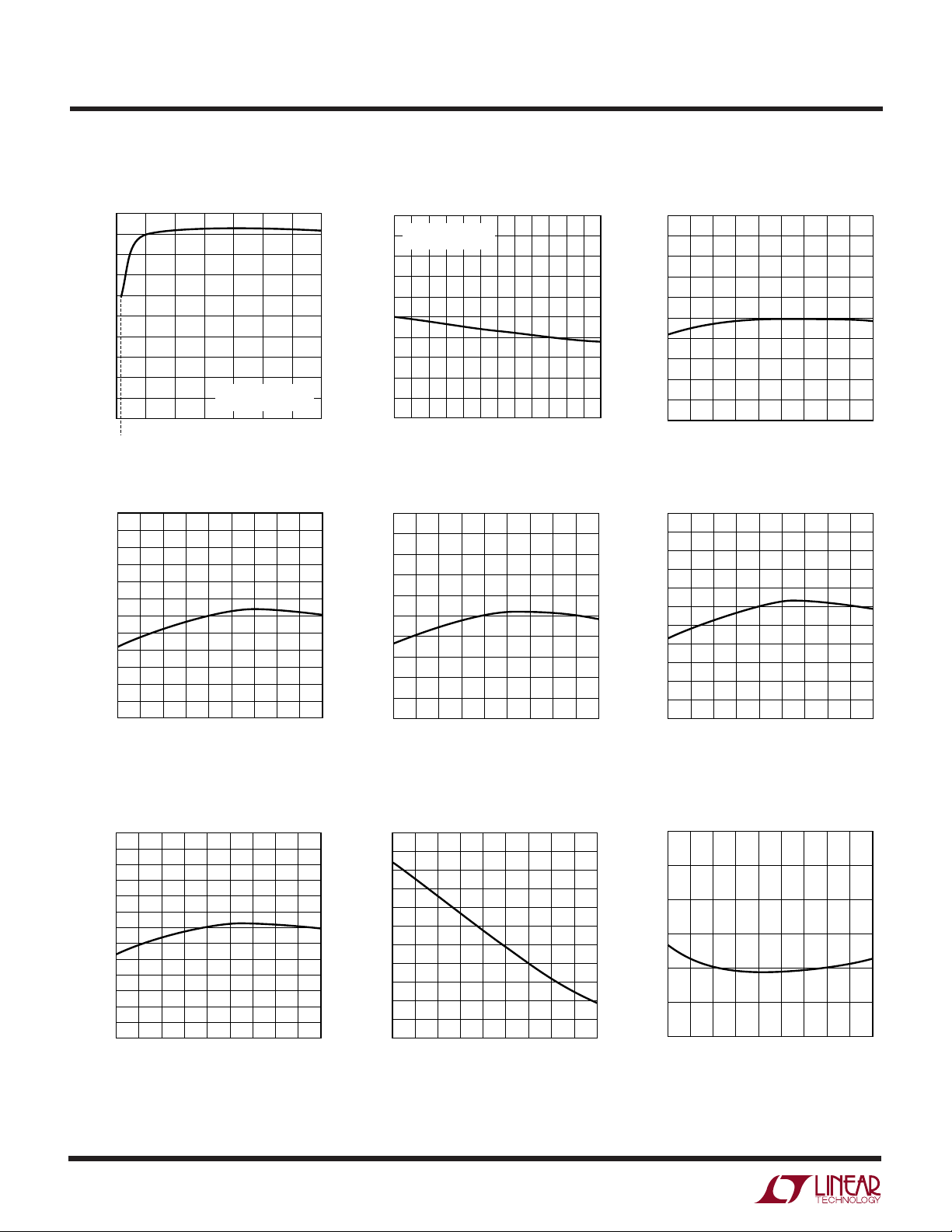
TYPICAL PERFOR A CE CHARACTERISTICS
Efficiency vs Load Current
100
90
80
70
60
50
40
EFFICIENCY (%)
30
20
10
0
0
0.3
4
2
LOAD CURRENT (A)
LTC1530-1.9 V
1.930
1.925
1.920
1.915
1.910
1.905
(V)
1.900
OUT
V
1.895
1.890
1.885
1.880
1.875
1.870
–55
–35
5
–15
TEMPERATURE (°C)
TA = 25°C
REFER TO FIGURE 10
8
6
OUT
25
10
vs Temperature
45 65 85 105 125
12
1530 G01
1530 G04
14
Load Regulation
2.510
TA = 25°C
2.508
REFER TO FIGURE 2
2.506
2.504
2.502
2.500
2.498
2.496
OUTPUT VOLTAGE (V)
2.494
2.492
2.490
0123456
OUTPUT CURRENT (A)
LTC1530-2.5 V
2.55
2.54
2.53
2.52
2.51
(V)
2.50
OUT
V
2.49
2.48
2.47
2.46
2.45
–35 5
–55
–15
TEMPERATURE (°C)
vs Temperature
OUT
85
45 125
25
65
1530 G02
105
1530 G05
LTC1530 V
1.260
1.255
1.250
1.245
1.240
(V)
1.235
SENSE
V
1.230
1.225
1.220
1.215
1.210
–55
LTC1530-2.8 V
2.85
2.84
2.83
2.82
2.81
2.80
(V)
OUT
2.79
V
2.78
2.77
2.76
2.75
2.74
–55
–15
–35 5
–35
–15
vs Temperature
SENSE
45 125
25
TEMPERATURE (°C)
5
TEMPERATURE (°C)
65
vs Temperature
OUT
25
45 65 85 105 125
85
105
1530 G03
1530 G06
4
(V)
OUT
V
3.36
3.35
3.34
3.33
3.32
3.31
3.30
3.29
3.28
3.27
3.26
3.25
3.24
3.23
LTC1530-3.3 V
–35
–55
–15
TEMPERATURE (°C)
vs Temperature
OUT
5
25
45 65 85 105 125
1530 G06
Undervoltage Lockout Threshold
Voltage vs Temperature
4.5
4.3
4.1
3.9
3.7
3.5
3.3
3.1
2.9
2.7
2.5
UNDERVOLTAGE LOCKOUT THRESHOLD (V)
2.3
–35 5
–55
–15
25
TEMPERATURE (°C)
45 125
65
Error Amplifier Transconductance
vs Temperature
2.8
2.6
2.4
2.2
2.0
1.8
1.6
ERROR AMPLIFIER TRANSCONDUCTANCE (millimho)
–35 5
–55
85
105
1530 G08
–15
25
TEMPERATURE (°C)
85
45 125
105
65
1530 G09
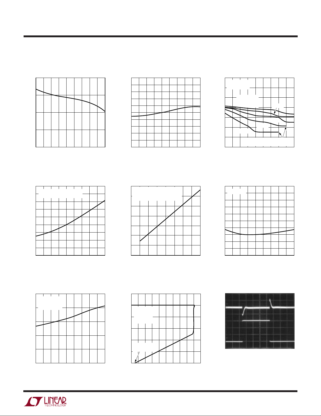
AMBIENT TEMPERATURE (°C)
–55
MAXIMUM G1 DUTY CYCLE (%)
92
90
88
86
84
82
80
78
–15
25
45 125
1530 G12
–35 5
65
85
105
THERMAL SHUTDOWN OCCURS
BEYOND THESE POINTS
G1, G2
CAPACITANCE
= 1000pF
PVCC = 12V
f
OSC
= 300kHz
7700pF
5500pF
3300pF
2200pF
TEMPERATURE (°C)
–55
80
75
70
65
60
55
50
45
40
35
30
–15
25
45 125
1530 G15
–35 5
65
85
105
PVCC = 12V
PV
CC
SHUTDOWN CURRENT (µA)
UW
TYPICAL PERFOR A CE CHARACTERISTICS
LTC1530
Error Amplifier Open-Loop Gain
vs Temperature
60
55
50
45
ERROR AMPLIFIER OPEN-LOOP DC GAIN (dB)
SINK CURRENT (µA)
MAX
I
40
300
280
260
240
220
200
180
160
140
120
–15
–35 5
–55
I
Sink Current vs Temperature
MAX
PVCC = 12V
G1, G2 ARE NOT SWITCHING
–15
–35 5
–55
25
TEMPERATURE (°C)
25
TEMPERATURE (°C)
85
45 125
65
85
45 125
65
105
105
1530 G10
1530 G13
Oscillator Frequency
vs Temperature
350
340
330
320
310
300
290
280
270
OSCILLATOR FREQUENCY (kHz)
260
250
–35 5
–55
–15
25
TEMPERATURE (°C)
PVCC Supply Current
vs Gate Capacitance
70
PVCC = 12V
= 25°C
T
A
60
GATE CAPACITANCE = C
50
40
30
SUPPLY CURRENT (mA)
20
CC
PV
10
0
1357
0
24 8
GATE CAPACITANCE (nF)
85
45 125
= C
G1
105
65
1530 G11
G2
6
1530 G14
Maximum G1 Duty Cycle
vs Ambient Temperature
PVCC Shutdown Supply Current
vs Temperature
Shutdown Threshold Voltage
vs Temperature Output Overcurrent Protection
250
PVCC = 12V
MEASURED AT
COMP PIN
200
150
100
50
SHUTDOWN THRESHOLD VOLTAGE (mV)
0
–35 5
–55
–15
TEMPERATURE (°C)
45 125
25
Transient Response
3.0
2.5
PVCC = 12V
T
= 25°C
A
2.0
REFER TO
FIGURE 2
1.5
1.0
OUTPUT VOLTAGE (V)
SHORT-CIRCUIT
CURRENT
0.5
85
105
65
1530 G16
0
213579
0
OUTPUT CURRENT (A)
6
4
8
1530 G17
50mV/DIV
2A/DIV
50µs/DIV 1530 G18
10
5

LTC1530
U
UU
PI FU CTIO S
PVCC (Pin 1): Power Supply for G1, G2 and Logic. PV
must connect to a potential of at least VIN + V
GS(ON)Q1
VIN = 5V, generate PVCC using a simple charge pump
connected to the switching node between Q1 and Q2 (see
Figure 1) or connect PVCC to a 12V supply. Bypass PV
properly or erratic operation will result. A low ESR 10µF
capacitor or larger bypass capacitor along with a 0.1µF
surface mount ceramic capacitor in parallel is recommended from PVCC directly to GND to minimize switching
ripple. Switching ripple should be ≤100mV at the PV
pin.
GND (Pin 2): Power and Logic Ground. GND is connected
to the internal gate drive circuitry and the feedback circuitry. To obtain good output voltage regulation, use
proper ground techniques between the LTC1530 GND and
bottom-side FET source and the negative terminal of the
output capacitor. See the Applications Information section
for more details on PCB layout techniques.
V
SENSE/VOUT
(Pin 3): Feedback Voltage Pin. For the adjust-
able LTC1530, use an external resistor divider to set the
required output voltage. Connect the tap point of the
resistor divider network to V
and the top of the
SENSE
divider network to the output voltage. For fixed output
voltage versions of the LTC1530, the resistor divider is
internal and the top of the resistor divider network is
brought out to V
. In general, the resistor divider
OUT
network for each fixed output voltage version sinks approximately 30µA. Connect V
to the output voltage
OUT
either at the output capacitors or at the actual point of load.
V
SENSE/VOUT
is sensitive to switching noise injected into
the pin. Isolate high current switching traces from this pin
and its PCB trace.
COMP (Pin 4): External Compensation. The COMP pin is
connected to the error amplifier output and the input of the
PWM comparator. An RC + C network is typically used at
CC
. If
CC
CC
COMP to compensate the feedback loop for optimum
transient response. To shut down the LTC1530, pull this
pin below 0.1V with an open-collector or open-drain
transistor. Supply current is typically reduced to 45µA in
shutdown. An internal 4µA pullup ensures start-up.
I
(Pin 5): Current Limit Threshold. Current limit is set
MAX
by the voltage drop across an external resistor connected
between the drain of Q1 and I
pared with the voltage across the R
. This voltage is com-
MAX
of the high side
DS(ON)
MOSFET. The LTC1530 contains a 200µA internal pull-
down at I
to set current limit. This 200µA current
MAX
source has a positive temperature coefficient to provide
first order correction for the temperature coefficient of the
external N-channel MOSFET’s R
DS(ON)
.
IFB (Pin 6): Current Limit Sense Pin. Connect IFB to the
switching node between Q1’s source and Q2’s drain. If I
drops below I
with G1 on, the LTC1530 enters current
MAX
FB
limit. Under this condition, the internal soft-start capacitor
is discharged and COMP is pulled low slowly. Duty cycle
is reduced and output power is limited. The current limit
circuitry is only activated if PVCC ≥ 8V. This action eases
start-up considerations as PVCC is ramping up because
the MOSFET’s R
can be significantly higher than
DS(ON)
what is measured under normal operating conditions. The
current limit circuit is disabled by floating I
and short-
MAX
ing IFB to PVCC.
G2 (Pin 7): Gate Drive for the Low Side N-Channel MOSFET,
Q2. This output swings from PVCC to GND. It is always low
if G1 is high or if the output is disabled. To prevent
undershoot during a soft-start cycle, G2 is held low until
G1 first transitions high.
G1 (Pin 8): Gate Drive for the Topside N-Channel MOSFET,
Q1. This output swings from PVCC to GND. It is always low
if G2 is high or if the output is disabled.
6
+
0.1µF
10µF
1530 F03
I
MAX
PV
CC
PV
CC
12V
GND
G1
NC
NC
NC
V
FB
I
FB
G2
V
SENSE/VOUT
COMPCOMP
LTC1530
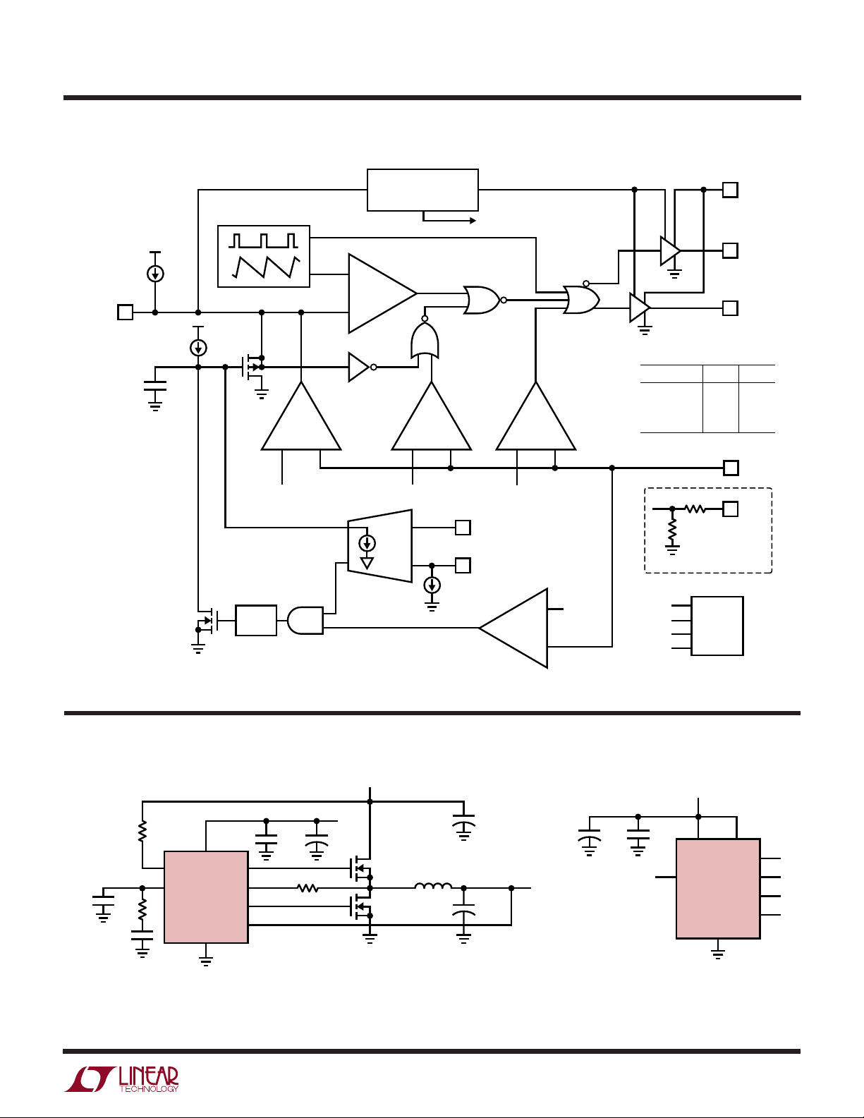
BLOCK DIAGRA
LTC1530
W
COMP
–
+ 3%
LVC
MAX
DISDR
+
–
1
PV
CC
G1
8
G2
7
OUT
R1
23.4k
44.4k
54.9k
68.4k
R2
43.2k
43.2k
43.2k
40.8k
FIXED V
1.9V
2.5V
2.8V
3.3V
+
FB
FB
R2
V
V
/2
REF
REF
V
– 3%
REF
+ 3%
V
REF
/2
V
REF
R1
FOR FIXED
VOLTAGE
VERSIONS
3
V
SENSE
3
V
OUT
V
REF
1530 BD
LOGIC AND
INTERNAL
OSCILLATOR
I
COMP
4
I
C
SS
MHCL
SS
HCL
MONO
M
SS
g
= 2millimho
m
ERR MIN
+
–
V
REF
THERMAL SHUTDOWN
–
PWM
+
V
REF
–
CC
+
–
– 3%
I
MAX
+
POWER DOWN
I
6
FB
I
5
MAX
V
REF
TEST CIRCUITS
V
IN
5V
+
C
***
PV
CC
12V
750Ω
PV
CC
I
MAX
C1
100pF
0.01µF
R
8.2k
C
C
C
COMP
LTC1530-2.5
GND
G1
I
FB
G2
V
OUT
*SUMIDA CDRH127-2R4
**AVX TPSE337M006R0100
***SANYO 10MV1200GX
0.1µF
+
100Ω
Figure 2
10µF
Q1
Si4410DY
Q2
Si4410DY
L
O
2.4µH
*
IN
1200µF
× 2
V
OUT
CO**
+
330µF
× 8
2.5V
6A
1530 F02
Figure 3
7
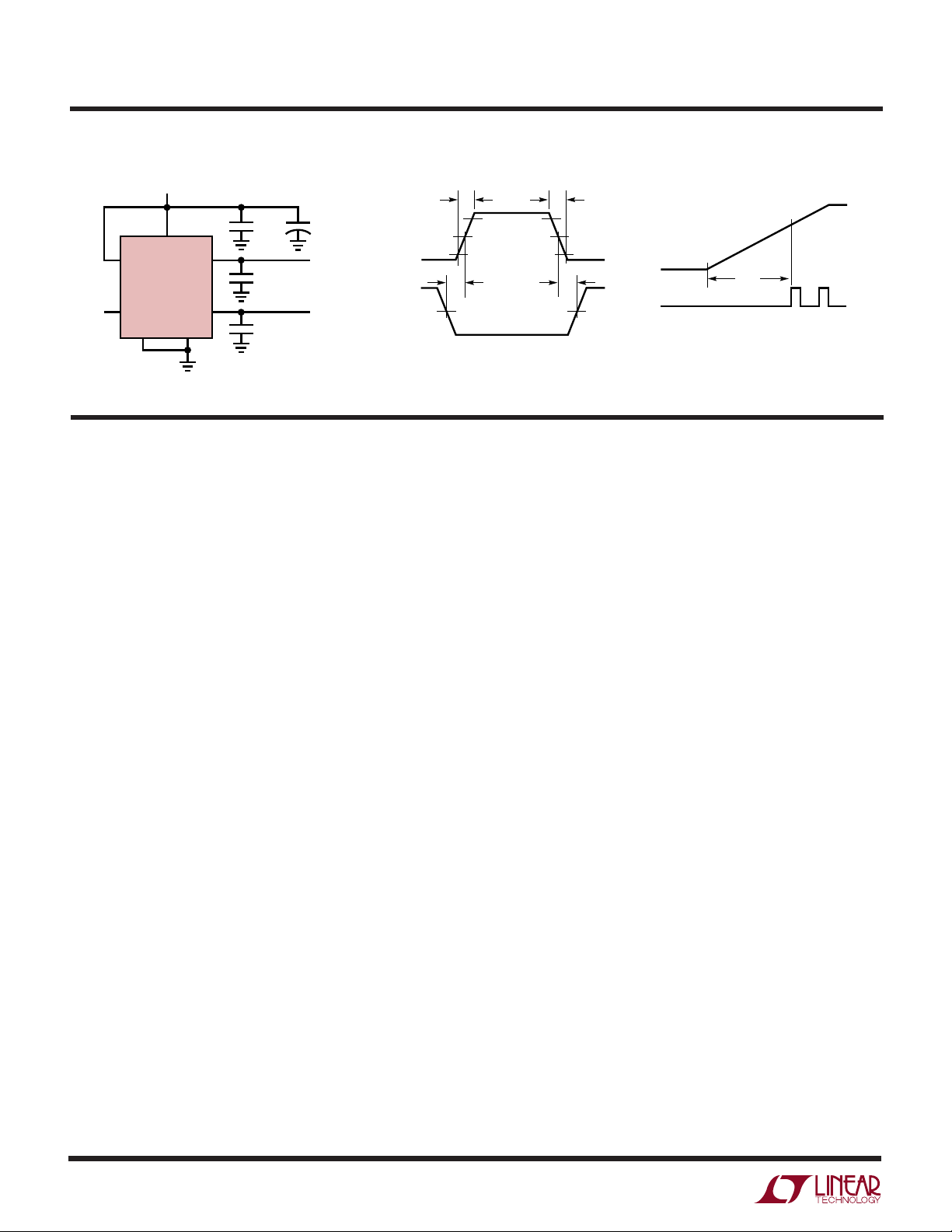
LTC1530
TEST CIRCUITS
PV
CC
12V
+
COMP
I
FB
COMP
V
OUT
PV
CC
LTC1530
GND
0.1µF
G1
3300pF
G2
3300pF
10µF
G1 RISE/FALL
G2 RISE/FALL
1530 F04a
WUUU
APPLICATIO S I FOR ATIO
t
r
90%
50%
10%
t
NOLtNOL
50%
Figure 4
90%
50%
10%
50%
t
f
COMP
G1
t
SS
1530 F04b
OVERVIEW
The LTC1530 is a voltage feedback, synchronous switching regulator controller (see Block Diagram) designed for
use in high power, low voltage step-down (buck) converters. It includes an on-chip soft-start capacitor, a PWM
generator, a precision reference trimmed to ±1%, two high
power MOSFET gate drivers and all the necessary feedback and control circuitry to form a complete switching
regulator circuit running at 300kHz.
The LTC1530 includes a current limit sensing circuit that
uses the topside external N-channel power MOSFET as a
current sensing element, eliminating the need for an
external sense resistor. If the current comparator, CC,
detects an overcurrent condition, the duty cycle is reduced
by discharging the internal soft-start capacitor through a
voltage-controlled current source. Under severe overloads or output short-circuit conditions, the soft-start
capacitor is pulled to ground and a start-up cycle is
initiated. If the short circuit or overload persists, the chip
repeats soft-start cycles and prevents damage to external
components.
THEORY OF OPERATION
Primary Feedback Loop
The LTC1530 compares the output voltage with the internal reference at the error amplifier inputs. The error
amplifier outputs an error signal to the PWM comparator.
This signal is compared to the fixed frequency oscillator
sawtooth waveform to generate the PWM signal. The
PWM signal drives the external MOSFETs at the G1 and G2
pins. The resulting chopped waveform is filtered by LO and
C
which closes the loop. Loop frequency compensa-
OUT
tion is typically accomplished with an external RC + C
network at the COMP pin, which is the output node of the
transconductance error amplifier.
MIN, MAX Feedback Loops
Two additional comparators in the feedback loop provide
high speed fault correction in situations where the error
amplifier cannot respond quickly enough. MIN compares
the feedback signal to a voltage 3% below the internal
reference. If the signal is below the comparator threshold,
the MIN comparator overrides the error amplifier and
forces the loop to maximum duty cycle, typically 86%.
Similarly, the MAX comparator forces the output to 0%
duty cycle if the feedback signal is greater than 3% above
the internal reference. To prevent these two comparators
from triggering due to noise, the MIN and MAX comparators’ response times are deliberately delayed by two to
three microseconds. These comparators help prevent
extreme output perturbations with fast output load current
transients, while allowing the main feedback loop to be
optimally compensated for stability.
Thermal Shutdown
The LTC1530 has a thermal protection circuit that disables
both internal gate drivers if activated. G1 and G2 are held
low and the LTC1530 supply current drops to about 1mA.
8
 Loading...