

Linear Technology LTC1520 Datasheet

Final Electrical Specifications
LTC1520
50Mbps Precision Quad
Line Receiver
FEATURES
■
Precision Propagation Delay: 18ns ±3ns Over
Temperature
■
Data Rate: 50Mbps
■
Low t
■
■
■
■
■
■
■
■
■
PLH/tPHL
Low Channel-to-Channel Skew: 400ps Typ
Rail-to-Rail Input Common Mode Range
High Input Resistance: ≥18k, Even When Unpowered
Hot Swap Capable
Can Withstand Input DC Levels of ±10V
Short-Circuit Protected
Single 5V Supply
LVDS Compatible
Will Not Oscillate with Slow Input Signals
Skew: 500ps Typ
U
APPLICATIONS
■
High Speed Backplane Interface
■
Line Collision Detector
■
PECL and LVDS Line Receivers
■
Level Translator
■
Ring Oscillator
■
Tapped Delay Line
, LTC and LT are registered trademarks of Linear Technology Corporation.
U
May 1996
DESCRIPTION
The LTC®1520 is a high speed, precision differential line
receiver that can operate at data rates as high as 50Mbps.
A unique architecture provides very stable propagation
delays and low skew over a wide input common mode,
input overdrive and ambient temperature range. Propagation delay is 18ns ± 3ns, while typically t
PLH/tPHL
500ps and channel-to-channel skew is 400ps.
Each receiver translates differential input levels (VID ≥
100mV) into valid CMOS and TTL output levels. Its high
input resistance (≥18k) allows many receivers to be connected to the same driver. The receiver outputs go into a
high impedance state when disabled.
Protection features include thermal shutdown and a controlled maximum short-circuit current (50mA max) that
does not oscillate in and out of short-circuit mode. Input
resistance remains ≥18k when the device is unpowered or
disabled, thus allowing the LTC1520 to be hot swapped into
a backplane without loading the data lines.
The LTC1520 operates from a single 5V supply and draws
12mA of supply current. The part is available in a 16-lead
narrow SO package.
skew is
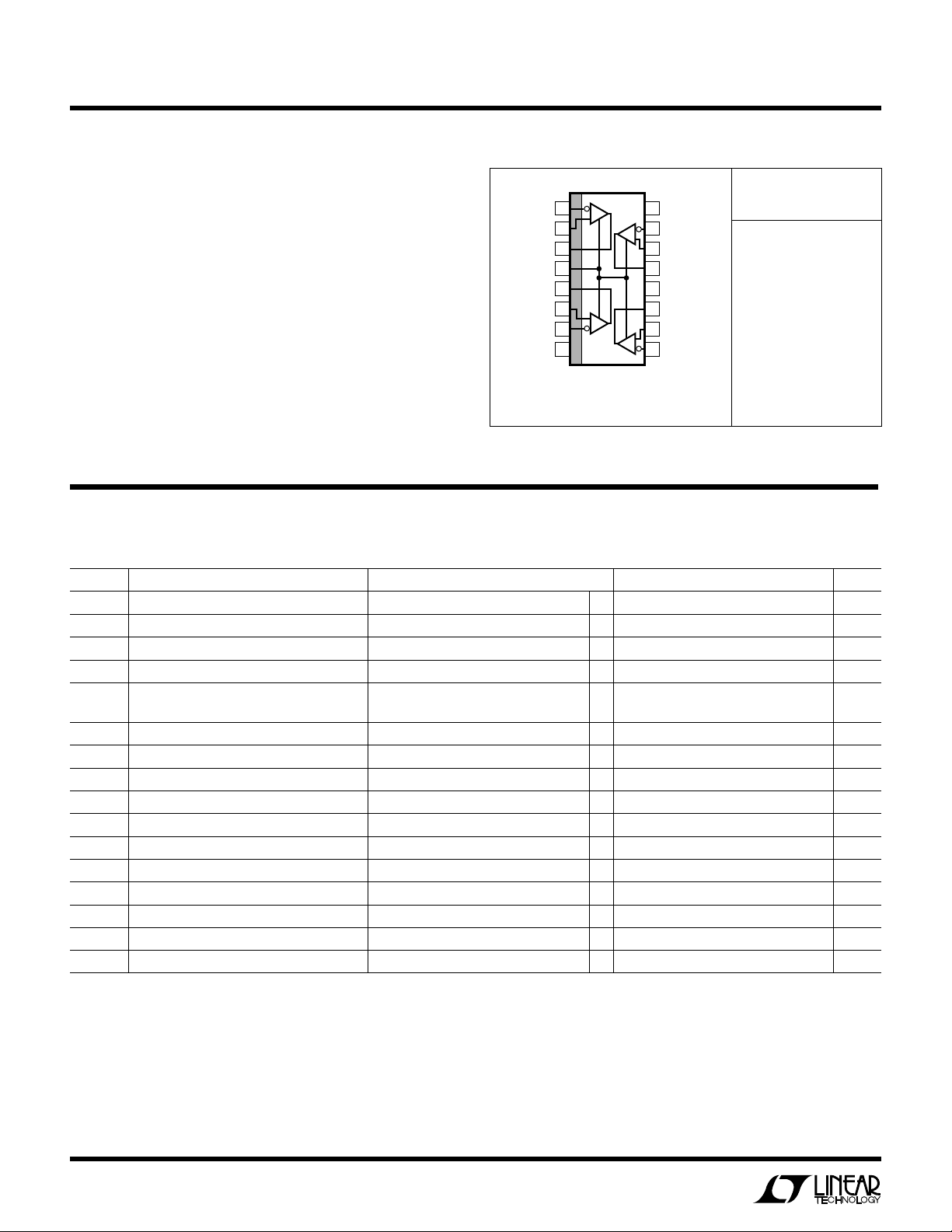
TYPICAL APPLICATION
High Speed Backplane Receiver
LTC1520
+
–
+
–
Information furnished by Linear Technology Corporation is believed to be accurate and reliable.
However, no responsibility is assumed for its use. Linear Technology Corporation makes no representation that the interconnection of its circuits as described herein will not infringe on existing patent rights.
U
+
–
+
–
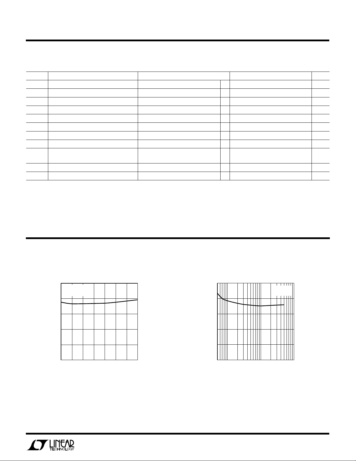
Propagation Delay Guaranteed to Fall
Within Shaded Area (±3ns)
RECEIVER
VIN =
1V/DIV
RECEIVER
OUTPUT
=
V
OUT
5V/DIV
5V
3.3k
3.3k
0.01µF
LTC1520 TA01
= 5V
V
DD
–5 5 15
TIME (ns)
INPUT
V
= 500mV
ID
25 350 1020304045
LTC1520 TA02
1
LTC1520
A
W
O
LUTEXI T
S
A
WUW
ARB
U
G
I
S
(Note 1)
Supply Voltage ....................................................... 10V
Digital Input Currents ..................... –100mA to 100mA
Digital Input Voltages ............................... –0.5V to 10V
Receiver Input Voltages ........................................ ±10V
Receiver Output Voltages ............. – 0.5V to VDD + 0.5V
Short-Circuit Duration .................................... Indefinite
Operating Temperature Range .................... 0°C to 70°C
Storage Temperature Range ................ –65°C to 150°C
Lead Temperature (Soldering, 10 sec)................. 300°C
DC ELECTRICAL CHARACTERISTICS
VDD = 5V (Notes 2, 3) per receiver, unless otherwise noted.
/
TOP VIEW
S PACKAGE
= 150°C, θ
O
RDER I FOR ATIO
ORDER PART
16
V
DD
15
B4
LTC1520CS
= 90°C/W
JA
14
A4
13
OUT 4
12
NC
11
OUT 3
10
A3
9
B3
PACKAGE
1
B1
2
A1
3
OUT 1
4
ENABLE
5
OUT 2
6
A2
7
B2
8
GND
16-LEAD PLASTIC SO
T
JMAX
Consult factory for Industrial and Military grade parts.
WU
U
NUMBER
SYMBOL PARAMETER CONDITIONS MIN TYP MAX UNITS
V
CM
V
IH
V
IL
I
IN1
I
IN2
R
IN
C
IN
V
OC
V
ID(MIN)
dV
ID
V
OH
V
OL
I
OZR
I
DD
I
OSR
CMRR Common Mode Rejection Ratio VCM = 2.5V, f = 25MHz 45 dB
Input Common Mode Voltage A, B Inputs ● –0.2 VDD + 0.2 V
Input High Voltage Enable Input ● 2V
Input Low Voltage Enable Input ● 0.8 V
Input Current Enable Input ● –1 1 µA
Input Current (A, B) VA, VB = 5V ● 250 µA
, VB = 0 ● –250 µA
V
A
Input Resistance (Figure 5) –0.2V ≤ VCM ≤ VDD + 0.2V ● 18 kΩ
A, B Input Capacitance 3pF
Open-Circuit Input Voltage (Figure 5) VDD = 5V (Note 4) ● 3.2 3.3 3.4 V
Differential Input Threshold Voltage –0.2V < VCM < VDD + 0.2V ● –0.1 0.1 V
Input Hysteresis VCM = 2.5V ● 20 mV
Output High Voltage I
Output Low Voltage I
Three-State Output Current 0V ≤ V
Total Supply Current All 4 Receivers VID ≥ 0.1V, No Load, Enable = 5V ● 12 20 mA
Short-Circuit Current V
= –4mA, VID = 0.1V, VDD = 5V ● 4.6 V
OUT
= 4mA, VID = 0.1V, VDD = 5V ● 0.4 V
OUT
≤ 5V ● –10 10 µA
OUT
OUT
= 0V, V
= 5V ● –50 50 mA
OUT
2
LTC1520
UW
SWITCHI G TI E CHARACTERISTICS
VDD = 5V (Notes 2, 3) VID = 500mV, VCM = 2.5V, unless otherwise noted.
SYMBOL PARAMETER CONDITIONS MIN TYP MAX UNITS
t
, t
PLH
tr, t
f
t
SKD
t
ZL
t
ZH
t
LZ
t
HZ
t
CH-CH
t
PKG-PKG
f
IN
Input-to-Output Propagation Delay CL = 15pF (Figure 1) ● 15 18 21 ns
PHL
Rise/Fall Times CL = 15pF 2.5 ns
t
– t
PLH
Skew C
PHL
= 15pF, Same Receiver (Note 5) ● 500 ps
L
Enable to Output Low CL = 15pF (Figure 2) ● 10 25 ns
Enable to Output High CL = 15pF (Figure 2) ● 10 25 ns
Disable from Output Low CL = 15pF (Figure 2) ● 20 35 ns
Disable from Output High CL = 15pF (Figure 2) ● 20 35 ns
Channel-to-Channel Skew CL = 15pF (Figure 3) (Note 6) ● 400 ps
Package-to-Package Skew CL = 15pF, Same Temperature 1.5 ns
(Figure 4, Note 4)
Minimum Input Pulse Width (Note 4) 12 ns
Maximum Input Frequency (Note 4) 40 MHz
The ● denotes specifications which apply over the full operating
temperature range.
Note 1: Absolute Maximum Ratings are those values beyond which the
safety of the device cannot be guaranteed. Recommended: V
= 5V ±5%.
DD
Note 2: All currents into the device pins are positive; all currents out of the
device pins are negative.
W
U
Note 3: All typicals are given for V
Note 4: Guaranteed by design, but not tested.
Note 5: Worst-case t
over the full operating temperature range.
Note 6: Maximum difference between any two t
single package over the full operating temperature range.
TYPICAL PERFORMANCE CHARACTERISTICS
Propagation Delay (t
vs Temperature
25
VCM = 2.5V
= 500mV
V
ID
20
15
10
PROPAGATION DELAY (ns)
5
PLH/tPHL
)
– t
PLH
skew for a single receiver in a package
PHL
Propagation Delay (t
vs Input Overdrive
25
20
15
10
PROPAGATION DELAY (ns)
5
= 5V, TA = 25°C.
DD
PLH/tPHL
TA = 25°C
V
PLH
CM
or t
)
= 2.5V
transitions in a
PHL
0
–50 –25
0
TEMPERATURE (°C)
50
25
100
LTC1520 G01
125
75
0
0.05
0.1 1 5 10
INPUT OVERDRIVE (V)
1520 G02
3
 Loading...