

Linear Technology LTC1519, LTC1518 Datasheet
FEATURES
■
Precision Propagation Delay: 18.5ns ±3.5ns Over
Temperature
■
High Data Rate:
■
Low t
■
■
■
■
PLH/tPHL
Low Channel-to-Channel Skew: 500ps Typ
–7V to 12V RS485 Input Common Mode Range
Input Resistance ≥22k, Even When Unpowered
Guaranteed Fail-Safe Operation over the Entire
52Mbps
Skew: 500ps Typ
Common Mode Range
■
Hot SwapTM Capable
■
High Common Mode Rejection to 26MHz
■
Short-Circuit Protection: 10mA Typ Output Current
for an Indefinite Short
■
Three-State Output Capability
■
Will Not Oscillate with Slow Moving Input Signals
■
Single 5V Supply
■
Pin Compatible with LTC488, LTC489
U
APPLICATIONS
■
High Speed RS485/RS422 Receivers
■
STS-1/OC-1 Data Receivers
■
PECL Line Receivers
■
Level Translators
■
Fast-20/Fast-40 SCSI Receiver
, LTC and LT are registered trademarks of Linear Technology Corporation.
Hot Swap is a trademark of Linear Technology Corporation.
LTC1518/LTC1519
52Mbps Precision Delay
RS485 Quad Line Receivers
U
DESCRIPTION
The LTC®1518/LTC1519 are high speed, precision delay
differential quad bus/line receivers that can operate at data
rates as high as 52Mbps. They are pin compatible with the
LTC488/LTC489 RS485 line receivers and operate over the
entire – 7V to 12V common mode range. A unique architecture provides very stable propagation delays and low skew
over wide input common mode, input overdrive and ambient temperature ranges. Propagation delay is 18.5ns
±3.5ns. Typical t
PLH/tPHL
500ps.
Each receiver translates differential input levels (VID ≥
300mV) into valid CMOS and TTL output levels. Its high
input resistance (≥22k) allows many receivers to be connected to the same driver. The receiver outputs go into a
high impedance state when disabled.
The receivers have a fail-safe feature that guarantees a high
output state when the inputs are shorted or left floating.
Other protection features include thermal shutdown and a
controlled maximum short-circuit current (50mA Max).
Input resistance remains ≥22k when the device is
unpowered or disabled, thus allowing hot swapping without loading the data lines.
The LTC1518/LTC1519 operate from a single 5V supply
and draw 12mA of supply current.
and channel-to-channel skew is
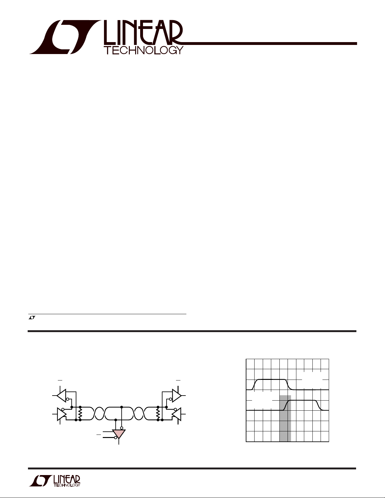
TYPICAL APPLICATION
52Mbps Data Communication over Twisted Pair
RE RE
2
1
RO
7
4
DI
3
DE
100Ω
6
A 1
4
EN
EN
12
2 B
3
RO
U
Propagation Delay Guaranteed to Fall
Within Shaded Area (±3.5ns)
RECEIVER
VIN =
2
1
RO
7
100Ω
1/4 LTC1518 LTC1685LTC1685
6
3
DE
1518/19 F08
4
DI
3V/DIV
=
V
OUT
5V/DIV
–5 5 15
RECEIVER
OUTPUT
= 5V
V
DD
TIME (ns)
INPUT
= 1.5V
V
ID
25 350 1020304045
1518/19 TA02
1
LTC1518/LTC1519
TOP VIEW
S PACKAGE
16-LEAD PLASTIC SO
1
2
3
4
5
6
7
8
16
15
14
13
12
11
10
9
B1
A1
OUT 1
EN12
OUT 2
A2
B2
GND
V
DD
B4
A4
OUT 4
EN34
OUT 3
A3
B3
A
W
O
LUTEXI TIS
S
A
WUW
U
ARB
G
(Note 1)
Supply Voltage ....................................................... 10V
Digital Input Currents ..................... –100mA to 100mA
Digital Input Voltages ............................... –0.5V to 10V
Receiver Input Voltages ........................................ ±14V
Receiver Output Voltages ............. –0.5V to VDD + 0.5V
PACKAGE
1
B1
2
A1
3
OUT 1
4
EN
5
OUT 2
6
A2
7
B2
8
GND
16-LEAD PLASTIC SO
T
= 150°C, θ
JMAX
/
O
RDER I FOR ATIO
TOP VIEW
16
V
DD
15
B4
14
A4
13
OUT 4
12
EN
11
OUT 3
10
A3
9
B3
S PACKAGE
= 90°C/W
JA
WU
ORDER PART
NUMBER
LTC1518CS
U
Receiver Input Differential ....................................... 10V
Short-Circuit Duration .................................... Indefinite
Operating Temperature Range .................... 0°C to 70°C
Storage Temperature Range ................ –65°C to 150°C
Lead Temperature (Soldering, 10 sec)................. 300°C
ORDER PART
NUMBER
LTC1519CS
T
JMAX
= 150°C, θ
= 90°C/W
JA
Consult factory for Industrial and Military grade parts.
DC ELECTRICAL CHARACTERISTICS
VDD = 5V ±5% (Notes 2, 3) per receiver, unless otherwise noted.
SYMBOL PARAMETER CONDITIONS MIN TYP MAX UNITS
V
CM
V
IH
V
IL
I
IN1
I
IN2
R
IN
C
IN
V
OC
V
ID(MIN)
dV
ID
V
OH
V
OL
I
OZR
I
DD
I
OSR
2
Input Common Mode Voltage A, B Inputs ● –7 12 V
Input High Voltage EN, EN, EN12, EN34 ● 2V
Input Low Voltage EN, EN, EN12, EN34 ● 0.8 V
Input Current EN, EN, EN12, EN34 ● –1 1 µA
Input Current (A, B) VA, VB = 12V ● 500 µA
, VB = –7V ● –500 µA
V
A
Input Resistance –7V ≤ VCM ≤ 12V (Figure 5) ● 22 kΩ
Input Capacitance (Note 4) 3 pF
Open-Circuit Input Voltage VDD = 5V (Note 4) (Figure 5) ● 3.2 3.3 3.4 V
Differential Input Threshold Voltage –7V ≤ VCM ≤ 12V ● –0.3 0.3 V
Input Hysteresis VCM = 2.5V 25 mV
Output High Voltage I
Output Low Voltage I
Three-State Output Current 0V < V
Total Supply Current All 4 Receivers VID > 0.3V, No Load, Device Enabled ● 12 20 mA
Short-Circuit Current V
= –4mA, VID = 0.3V, VDD = 5V ● 4.6 V
OUT
= 4mA, VID = –0.3V, VDD = 5V ● 0.4 V
OUT
< 5V ● –10 10 µA
OUT
OUT
= 0V, V
= 5V (Note 7) ● –50 50 mA
OUT
LTC1518/LTC1519
DC ELECTRICAL CHARACTERISTICS
VDD = 5V ±5% (Notes 2, 3) per receiver, unless otherwise noted.
SYMBOL PARAMETER CONDITIONS MIN TYP MAX UNITS
Max VID for Fail-Safe Detection –7V ≤ VCM ≤ 12V 25 mV
Min Time to Detect Fault Condition 2 µs
CMRR Common Mode Rejection Ratio VCM = 2.5V, f = 26MHz (Note 4) 45 dB
UW
SWITCHI G TI E CHARACTERISTICS
VDD = 5V ±5% (Notes 2, 3) VID = 1.5V, VCM = 2.5V, unless otherwise noted.
SYMBOL PARAMETER CONDITIONS MIN TYP MAX UNITS
t
, t
PLH
tr, t
f
t
SKD
t
ZL
t
ZH
t
LZ
t
HZ
t
CH-CH
t
PKG-PKG
tr, tf Input Maximum Input Rise or Fall Time (Note 4) ● 2000 ns
f
IN(MAX)
C
L
The ● denotes specifications which apply over the full operating
temperature range.
Note 1: Absolute Maximum Ratings are those values beyond which the life
of a device may be impaired.
Note 2: All currents into the device pins are positive; all currents out of the
device pins are negative.
Note 3: All typicals are given for V
Note 4: Guaranteed by design, but not tested.
Input-to-Output Propagation Delay CL = 15pF (Figure 1) ● 15 18.5 22 ns
PHL
Rise/Fall Times CL = 15pF 2.5 ns
t
– t
PLH
Enable to Output Low CL = 15pF (Figure 2) ● 10 35 ns
Enable to Output High CL = 15pF (Figure 2) ● 10 35 ns
Disable from Output Low CL = 15pF (Figure 2) ● 20 35 ns
Disable from Output High CL = 15pF (Figure 2) ● 20 35 ns
Channel-to-Channel Skew CL = 15pF (Figure 3, Note 6) 500 ps
Package-to-Package Skew CL = 15pF, Same Temperature 1.5 ns
Minimum Input Pulse Width (Note 4) ● 12 19.2 ns
Maximum Input Frequency Square Wave (Note 4) ● 26 40 MHz
Maximum Data Rate (Note 4) ● 52 80 Mbps
Load Capacitance (Note 4) 500 pF
Skew C
PHL
= 5V, TA = 25°C.
DD
= 15pF, Same Receiver (Note 5) 500 ps
L
(Figure 4, Note 4)
t
– t
Note 5: Worst-case
over the full operating temperature range.
Note 6: Maximum difference between any two t
single package over the full operating temperature range.
Note 7: Short-circuit current does not represent output drive capability.
When the output detects a short-circuit condition, output drive current is
significantly reduced until the short is removed.
PLH
skew for a single receiver in a package
PHL
or t
PLH
transitions in a
PHL
3
LTC1518/LTC1519
DATA RATE (Mbps)
0
SUPPLY CURRENT (mA)
50
45
40
35
30
25
20
15
10
5
0
40
LTC1518/19 • TPC05
10
20
30
50
TA = 25°C
V
CM
= 2.5V
V
ID
= 1.5V
4 RECEIVERS
SWITCHING
1 RECEIVER
SWITCHING
COMMON MODE (V)
–6
PROPAGATION DELAY (ns)
25
20
15
10
5
0
–2
2
412
LTC1464 • TPC08
–4 0
6
8
10
TA = 25°C
V
ID
= 1.5V
INPUT DIFFERENTIAL (V)
0.3
DATA RATE (Mbps)
70
60
50
40
30
20
10
0
0.5 1.0 1.5 2.0
LTC1518/19 • TPC10
2.5
TA = 25°C
V
CM
= 2.5V
W
U
TYPICAL PERFORMANCE CHARACTERISTICS
Propagation Delay (t
CMRR vs Frequency Supply Current vs Data Rate
46.5
46.0
45.5
45.0
44.5
44.0
43.5
43.0
TA = 25°C
42.5
COMMON MODE REJECTION RATIO (dB)
42.0
= 2.5V
V
CM
10
1k 100k 10M
FREQUENCY (Hz)
1518/19 G01
Supply Current
vs Temperature and Data Rate
25
1 RECEIVER
SWITCHING
20
15
10
SUPPLY CURRENT (mA)
5
0
100°C
25°C
–25°C
0°C
= 2.5V
V
CM
= 1.5V
V
ID
10
0
DATA RATE (Mbps)
30
40
20
50
LTC1518/19 • TPC06
vs Temperature
25
VCM = 2.5V
= 1.5V
V
ID
20
15
10
PROPAGATION DELAY (ns)
5
0
–50 –25
0
TEMPERATURE (°C)
Propagation Delay
vs Load Capacitance
30
TA = 25°C
= 2.5V
V
CM
25
= 1.5V
V
ID
20
15
10
PROPAGATION DELAY (ns)
5
0
5 15 25 35 55 105 205
LOAD CAPACITANCE (pF)
PLH/tPHL
50
25
75
100
LTC1518/19 • TPC07
)
125
1518/19 G02
Propagation Delay
vs Common Mode
4
Propagation Delay
vs Input Differential Voltage
25
TA = 25°C
= 2.5V
V
CM
20
15
10
PROPAGATION DELAY (ns)
5
0
0.5 1.0 1.5 2.0
0.3
INPUT DIFFERENTIAL (V)
Maximum Data Rate
vs Input Differential Voltage
2.5
LTC1518/19 • TPC09
 Loading...