

Linear Technology LTC1516 Datasheet
FEATURES
OUTPUT CURRENT (mA)
50
60
70
80
90
EFFICIENCY (%)
100
1516 • TA01
0.01 0.1 1 10
SHDN = 0V
V
IN
= 3V
LOW IQ MODE
(SEE FIGURE 3)
LTC1516
Micropower, Regulated
5V Charge Pump
DC/DC Converter
U
DESCRIPTION
■
Ultralow Power: Typical Operating ICC = 12µA
■
Short Circuit/Thermal Protection
■
Regulated 5V ±4% Output
■
2V to 5V Input Range
■
No Inductors
■
ICC in Shutdown: <1µA
■
Output Current:20mA (VIN > 2V)
50mA (VIN > 3V)
■
Shutdown Disconnects Load from V
■
Internal Oscillator: 600kHz
■
Compact Application Circuit (0.1 in2)
■
8-Pin SO Package
IN
U
APPLICATIONS
■
2-Cell to 5V Conversion
■
Li-Ion Battery Backup Supplies
■
Local 3V to 5V Conversion
■
5V Flash Memory Programmer
■
Smart Card Readers
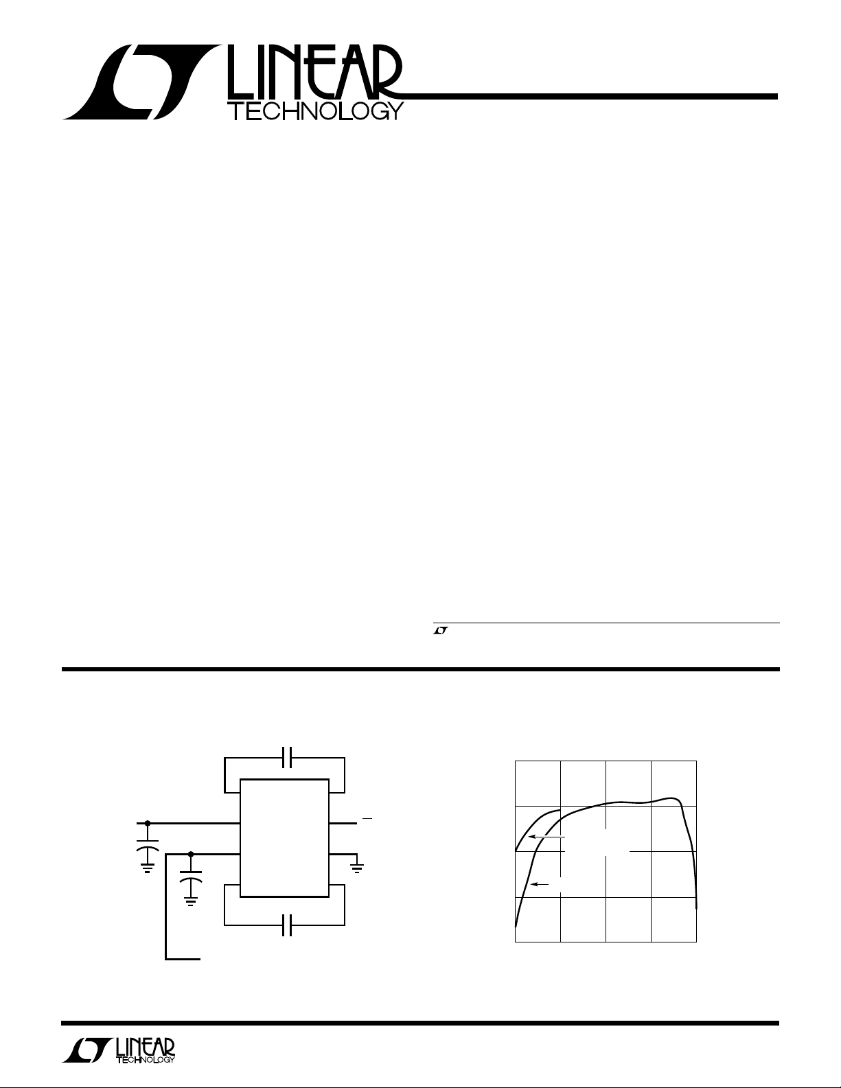
The LTC®1516 is a micropower charge pump DC/DC
converter that produces a regulated 5V output from a 2V
to 5V supply. Extremely low supply current (12µ A typical
with no load, <1µA in shutdown) and low external parts
count (two 0.22µ F flying capacitors and two 10µ F capacitors at VIN and V
) make the LTC1516 ideally suited for
OUT
small, light load battery-powered applications. Typical
efficiency (VIN = 3V) exceeds 70% with load currents
between 50µ A and 50mA. Modulating the SHDN pin keeps
the typical efficiency above 70% with load currents all the
way down to 10µA.
The LTC1516 operates as either a doubler or a tripler
depending on VIN and output load conditions to improve
overall efficiency. The part has thermal shutdown and can
survive a continuous short from V
to GND. In shut-
OUT
down the load is disconnected from VIN.
The LTC1516 is available in an 8-pin SO package in both
commercial and industrial temperature grades.
, LTC and LT are registered trademarks of Linear Technology Corporation.
TYPICAL APPLICATION
VIN = 2V TO 5V
Figure 1. Regulated 5V Output from a 2V to 5V Input
U
0.22µF
1
C1+
2
V
+
10µF
+
10µF
V
I
OUT
I
OUT
IN
LTC1516
3
V
OUT
4
+
C2
0.22µF
= 5V ±4%
OUT
= 0mA TO 20mA, VIN ≥ 2V
= 0mA TO 50mA, VIN ≥ 3V
C1–
SHDN
GND
C2
8
7
ON/OFF
6
5
–
1516 • F01
Efficiency vs Output Current
1
LTC1516
WW
W
ABSOLUTE MAXIMUM RATINGS
U
U
W
PACKAGE/ORDER INFORMATION
(Note 1)
VIN to GND...................................................–0.3V to 6V
V
to GND ................................................–0.3V to 6V
OUT
SHDN to GND ..............................................–0.3V to 6V
V
Short-Circuit Duration............................. Indefinite
OUT
Operating Temperature Range
Commercial .............................................0°C to 70°C
Industrial ............................................ –40°C to 85°C
Storage Temperature Range................. –65°C to 150°C
Lead Temperature (Soldering, 10 sec)..................300°C
TOP VIEW
–
1
C1+
V
2
IN
V
3
OUT
+
C2
4
S8 PACKAGE
8-LEAD PLASTIC SO
T
= 125°C, θJA = 150°C/W
JMAX
Consult factory for Military grade parts.
C1
8
SHDN
7
GND
6
–
C2
5
ORDER PART
NUMBER
LTC1516CS8
LTC1516IS8
S8 PART MARKING
1516
1516I
ELECTRICAL CHARACTERISTICS
VIN = 2V to 5V, C1 = C2 = 0.22µF, CIN = C
SYMBOL PARAMETER CONDITIONS MIN TYP MAX UNITS
V
IN
V
OUT
I
CC
f
OSC
V
IH
V
IL
I
IH
I
IL
t
ON
The ● denotes specifications which apply over the full operating
temperature range.
Note 1: Absolute Maximum Ratings are those values beyond which the life
of the device may be impaired
Input Voltage ● 25V
Output Voltage 2V ≤ VIN ≤ 5V, I
Supply Current 2V ≤ VIN ≤ 5V, I
Output Ripple Full Load 100 mV
Efficiency VIN = 3V, I
Switching Frequency Full Load 600 kHz
SHDN Input Threshold ● (0.7)(VIN)V
SHDN Input Current V
V
Turn-On Time VIN = 3V, I
OUT
= 10µF, T
OUT
≤ V
≤ 3.6V, I
3V
IN
3.6V ≤ VIN ≤ 5V, I
2V ≤ VIN ≤ 5V, I
= V
SHDN
V
= 0V ● –1 1 µA
SHDN
to T
MIN
OUT
OUT
OUT
OUT
OUT
= 20mA 82 %
OUT
IN
= 0mA (Note 3) 500 µs
OUT
unless otherwise specified (Note 3).
MAX
≤ 20mA ● 4.8 5.2 V
≤ 50mA ● 4.8 5.2 V
≤ 50mA, TA = 25°C (Note 2) 4.8 5.2 V
= 0mA, SHDN = 0V ● 12 20 µA
= 0mA, SHDN = V
Note 2: At input voltages >3.6V and ambient temperatures >70°C,
continuous power dissipation must be derated to maintain junction
temperatures below 125°C. Derate 6mW/°C above 70°C in SO-8.
Note 3: The LTC1516 is tested with the capacitors shown in Figure 1.
IN
● 0.005 1 µA
● 0.4 V
● –1 1 µA
U
2
W
U
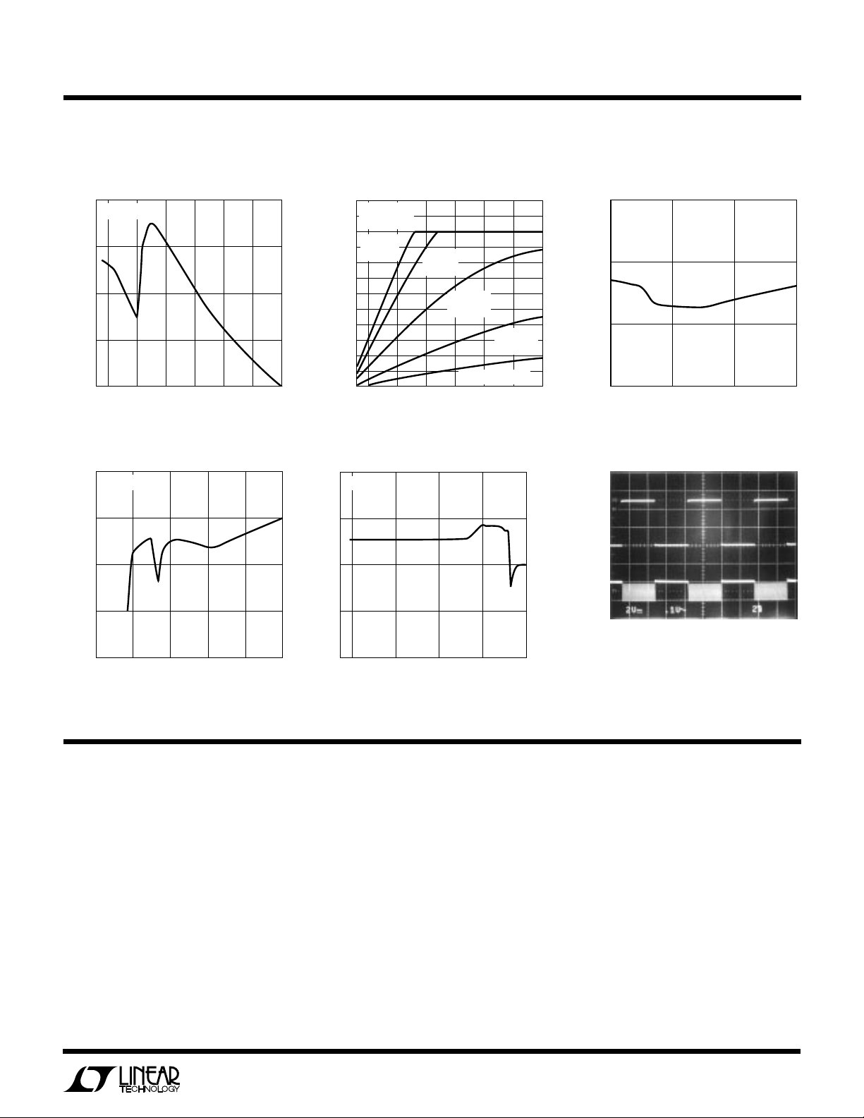
TYPICAL PERFORMANCE CHARACTERISTICS
Efficiency vs Input Voltage
90
= 10mA
I
OUT
80
Output Current vs Input Voltage
120
C
= 10µF
OUT
= 25°C
T
A
100
C1 = C2
80
= 0.22µF
C1 = C2
= 0.1µF
LTC1516
No Load Supply Current vs
Input Voltage
20
15
70
EFFICIENCY (%)
60
50
2.0 2.5 3.0 4.0 4.53.5
INPUT VOLTAGE (V)
Output Voltage vs Input Voltage
5.10
5.05
5.00
OUTPUT VOLTAGE (V)
4.95
4.90
= 20mA
I
OUT
2134
INPUT VOLTAGE (V)
1516 • G01
1516 • G04
5.0
5.10
5.05
5.00
OUTPUT VOLTAGE (V)
4.95
4.90
65
60
40
20
MAXIMUM OUTPUT CURRENT (mA)
0
234
C1 = C2
= 0.047µF
C1 = C2 = 0.01µF
INPUT VOLTAGE (V)
C1 = C2
= 0.022µF
Output Voltage vs Output Current
VIN = 3V
0.01 0.1 1 10 100
OUTPUT CURRENT (mA)
1516 • G05
1516 • G02
5
0mA TO 25mA,
10mA/DIV
AC COUPLED,
100mV/DIV
10
SUPPLY CURRENT (µA)
5
234
INPUT VOLTAGE (V)
Load Transient Response, VIN = 3V
I
,
OUT
V
,
OUT
1516 • G03
1516 • G04
5
UUU
PIN FUNCTIONS
C1+ (Pin 1): Flying Capacitor 1, Positive Terminal.
VIN (Pin 2): Input Supply Voltage.
V
(Pin 3): 5V Output Voltage (V
OUT
C2+ (Pin 4): Flying Capacitor 2, Positive Terminal.
C2– (Pin 5): Flying Capacitor 2, Negative Terminal.
= 0V in Shutdown).
OUT
GND (Pin 6): Ground.
SHDN (Pin 7): Active High CMOS Logic-Level Shutdown
Input.
C1– (Pin 8): Flying Capacitor 1, Negative Terminal.
3
 Loading...