

Linear Technology LTC1503-2, LTC1503-1.8 Datasheet
1
LTC1503-1.8/LTC1503-2
High Efficiency Inductorless
Step-Down DC/DC Converters
■
Input Voltage Range: 2.4V to 6V
■
Fixed Output Voltages: 1.8V ±4%, 2V ±4%
■
Output Current: Up to 100mA
■
No Inductors
■
Typical Efficiency 25% Higher than LDOs
■
Low Operating Current: 25µA
■
Low Shutdown Current: 5µA
■
600kHz Switching Frequency
■
Shutdown Disconnects Load from V
IN
■
Soft-Start Limits Inrush Current at Turn-On
■
Short-Circuit and Overtemperature Protected
■
Available in 8-Pin MSOP and SO Packages
The LTC®1503-1.8/LTC1503-2 are switched capacitor
step-down DC/DC converters that produce a regulated
output from a 2.4V to 6V input. The parts use switched
capacitor fractional conversion to achieve high efficiency
over the entire input range. No inductors are required.
Internal circuitry controls the step-down conversion ratio
to optimize efficiency as the input voltage and load conditions vary. Typical efficiency is 25% higher than that of a
low dropout (LDO) linear regulator.
Regulation is achieved by sensing the output voltage and
enabling the internal switching network as needed to
maintain a fixed output voltage. This method of regulation
enables the parts to achieve high efficiency at extremely
light loads. Low operating current (25µA with no load, 5µA
in shutdown) and low external parts count (two 1µF flying
capacitors and two 10µF bypass capacitors) make the
LTC1503-1.8/LTC1503-2
ideally suited for space constrained battery-powered applications. The parts are fully
short-circuit and overtemperature protected.
The
LTC1503-1.8/
LTC1503-2 are available in 8-pin MSOP
and SO packages.
, LTC and LT are registered trademarks of Linear Technology Corporation.
■
Cellular Phones
■
Handheld Computers
■
Smart Card Readers
■
Low Power DSP Supplies
■
Portable Electronic Equipment
■
Handheld Medical Instruments
Efficiency vs Input Voltage
Single Li-Ion to 2V DC/DC Converter
FEATURES
DESCRIPTIO
U
APPLICATIO S
U
TYPICAL APPLICATIO
U
4
2
3
5
1
8
6
7
V
IN
C1
–
C1
+
SHDN/SS
V
OUT
C2
–
C2
+
GND
LTC1503-2
1µF
1503-1.8/2 TA01
1µF
10µF
1-CELL Li-Ion OR
3-CELL NiMH
10µF
V
OUT
= 2V
I
OUT
= 100mA
INPUT VOLTAGE (V)
2
EFFICIENCY (%)
60
80
6
1503-1.8/2 TA02
40
20
3
4
5
100
LTC1503-2
V
OUT
= 2V
I
OUT
= 100mA
I
OUT
= 1mA
“IDEAL” LDO
2
LTC1503-1.8/LTC1503-2
Industrial Temperature Range ............... –40°C to 85°C
Specified Temperature Range (Note 2)... – 40°C to 85°C
Storage Temperature Range ................ –65°C to 150°C
Lead Temperature (Soldering, 10 sec)................. 300°C
(Note 1)
PARAMETER CONDITIONS MIN TYP MAX UNITS
VIN Operating Voltage ● 2.4 6 V
V
OUT
LTC1503-1.8, 0mA < I
OUT
< 100mA ● 1.728 1.8 1.872 V
LTC1503-2, 0mA < I
OUT
< 100mA ● 1.920 2.0 2.080 V
VIN Operating Current I
OUT
= 0mA ● 25 50 µA
VIN Shutdown Current SHDN/SS = 0V ● 510 µA
Output Ripple Voltage LTC1503-X, VIN = 3.6V, I
OUT
= 100mA 25 mV
P-P
Efficiency LTC1503-2, VIN = 3.6V, I
OUT
= 100mA 82.9 %
Switching Frequency Oscillator Free Running 600 kHz
SHDN/SS Input Threshold ● 0.2 0.35 0.5 V
SHDN/SS Input Current V
SHDN/SS
= 0V (Note 3) ● –3.5 –2 –1 µA
V
SHDN/SS
= V
IN
● –1 1 µA
V
OUT
Short-Circuit Current V
OUT
= 0V (Note 4) ● 82250 mA
V
OUT
Turn-On Time CSS = 0nF, VIN = 3.6V, C
OUT
= 10µF 0.1 ms
C
SS
= 10nF 8 ms
Note 1: Absolute Maximum Ratings are those values beyond which the life
of a device may be impaired.
Note 2: The LTC1503C is guaranteed to meet specified performance from
0°C to 70°C and is designed, characterized and expected to meet these
extended temperature limits, but are not tested at –40°C and 85°C. The
LTC1503I is guaranteed to meet the extended temperature limits.
Note 3: Currents flowing into the device are positive polarity. Currents
flowing out of the device are negative polarity.
Note 4: When V
OUT
is less than 150mV, I
OUT
is limited to much less than
the maximum rated output current to prevent damage to the output
devices.
ORDER PART
NUMBER
LTC1503CMS8-1.8
LTC1503CMS8-2
MS8 PART MARKING
LTFX
LTHN
ORDER PART
NUMBER
LTC1503CS8-1.8
LTC1503CS8-2
LTC1503IS8-1.8
LTC1503IS8-2
S8 PART MARKING
150318
15032
Consult factory for Military grade parts.
T
JMAX
= 125°C, θJA = 200°C/W
1
2
3
4
V
OUT
C1
–
C1
+
V
IN
8
7
6
5
C2
–
GND
C2
+
SHDN/SS
TOP VIEW
MS8 PACKAGE
8-LEAD PLASTIC MSOP
T
JMAX
= 125°C, θJA = 150°C/W
1
2
3
4
8
7
6
5
TOP VIEW
S8 PACKAGE
8-LEAD PLASTIC SO
V
OUT
C1
–
C1
+
V
IN
C2
–
GND
C2
+
SHDN/SS
VIN, C1+, C1–, C2+, C2– to GND............... –0.3V to 6.5V
SHDN/SS to GND......................... –0.3V to (VIN + 0.3V)
V
OUT
Short-Circuit Duration............................. Indefinite
Commercial Temperature Range ............ –40°C to 85°C
The ● denotes specifications which apply over the full operating temperature range, otherwise specifications are at TA = 25°C.
VIN = V
IN(MIN)
to V
IN(MAX)
, C1 = C2 = 1µF, CIN = C
OUT
= 10µF unless otherwise noted.
503I18
1503I2
ABSOLUTE AXI U RATI GS
WWWU
PACKAGE/ORDER I FOR ATIO
UU
W
ELECTRICAL CHARACTERISTICS
3
LTC1503-1.8/LTC1503-2
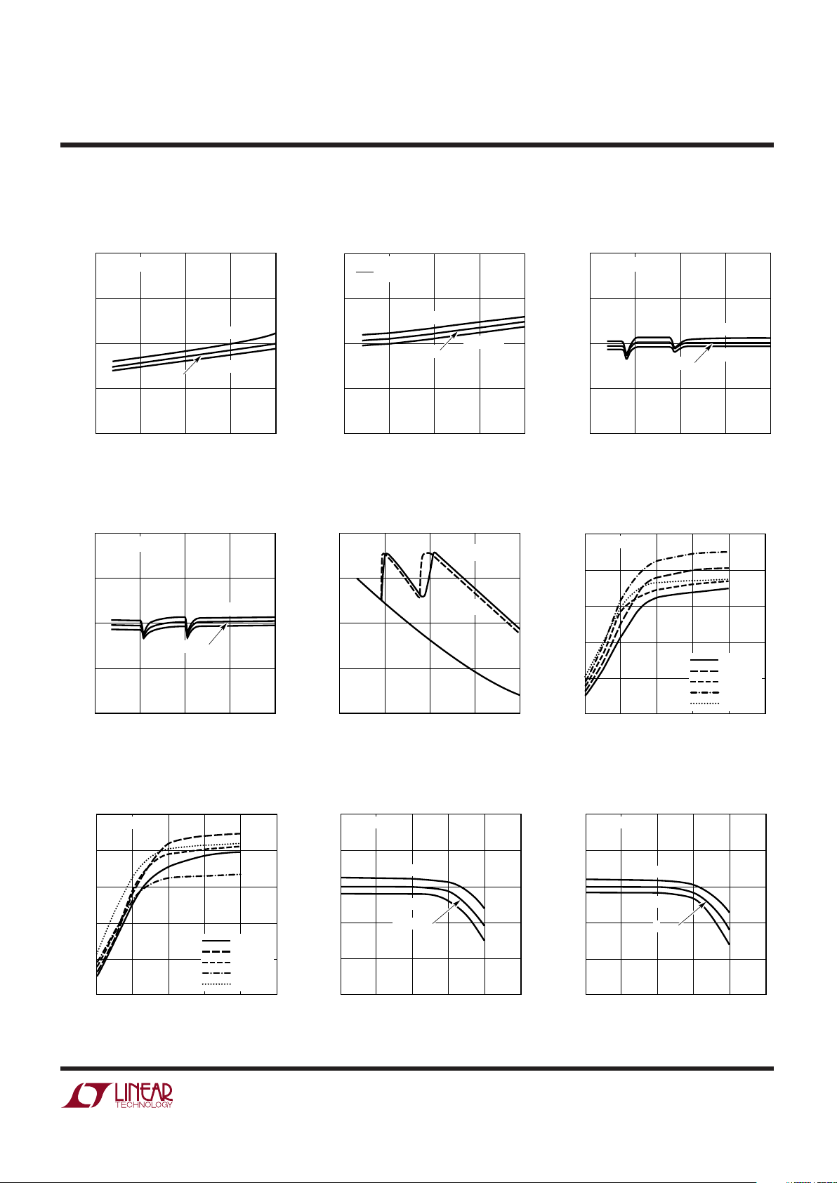
LTC1503-X Input Operating
Current vs Input Voltage
INPUT VOLTAGE (V)
2
INPUT CURRENT (µA)
30
T
A
= 25°C
40
6
1503 G01
20
10
3
4
5
50
I
OUT
= 0mA
TA = –40°C
T
A
= 85°C
LTC1503-1.8
Output Voltage vs Input Voltage
LTC1503-2
Output Voltage vs Input Voltage
LTC1503-1.8
Efficiency vs Input Voltage
INPUT VOLTAGE (V)
2
OUTPUT VOLTAGE (V)
2.00
2.05
6
1503 G03
1.95
1.90
3
4
5
2.10
I
OUT
= 50mA
TA = –40°C
T
A
= 85°C
T
A
= 25°C
INPUT VOLTAGE (V)
2
EFFICIENCY (%)
60
80
6
1503-1.8/2 G05
40
20
3
4
5
100
“IDEAL”
LDO
TA = 25°C
I
OUT
= 100mA
I
OUT
= 1mA
LTC1503-1.8
Efficiency vs Output Current
LTC1503-X Input Shutdown
Current vs Input Voltage
INPUT VOLTAGE (V)
2
INPUT SHUTDOWN CURRENT (µA)
5
7.5
6
1503-1.8/2 TA02
2.5
0
3
4
5
10
V
OUT
= 0V
V
SHDN
/SS = 0V
TA = –40°C
T
A
= 85°C
T
A
= 25°C
INPUT VOLTAGE (V)
2
OUTPUT VOLTAGE (V)
1.80
1.85
6
1503-1.8/2 G03
1.75
1.70
3
4
5
1.90
I
OUT
= 50mA
TA = –40°C
T
A
= 85°C
TA = 25°C
OUTPUT CURRENT (mA)
0.01
EFFICIENCY (%)
60
80
100
100
1503-1.8/2 G06
40
20
0
0.1
1
10
1000
VIN = 5V
V
IN
= 4.4V
V
IN
= 3.6V
V
IN
= 3V
V
IN
= 2.4V
TA = 25°C
LTC1503-2
Efficiency vs Output Current
OUTPUT CURRENT (mA)
0.01
EFFICIENCY (%)
60
80
100
100
1503-1.8/2 G07
40
20
0
0.1
1
10
1000
VIN = 5V
V
IN
= 4.4V
V
IN
= 3.6V
V
IN
= 3V
V
IN
= 2.4V
TA = 25°C
LTC1503-1.8
Output Voltage vs Output Current
OUTPUT CURRENT (mA)
0.01
OUTPUT VOLTAGE (V)
1.80
1.82
1.84
100
1503-1.8/2 G08
1.78
1.76
1.74
0.1
1
10
1000
VIN = 3.3V
TA = –40°C
TA = 85°C
T
A
= 25°C
LTC1503-2
Output Voltage vs Output Current
OUTPUT CURRENT (mA)
0.01
OUTPUT VOLTAGE (V)
2.00
2.02
2.04
100
1503-1.8/2 G09
1.98
1.96
1.94
0.1
1
10
1000
VIN = 3.3V
TA = –40°C
TA = 85°C
T
A
= 25°C
TYPICAL PERFOR A CE CHARACTERISTICS
UW
4
LTC1503-1.8/LTC1503-2
TYPICAL PERFOR A CE CHARACTERISTICS
UW
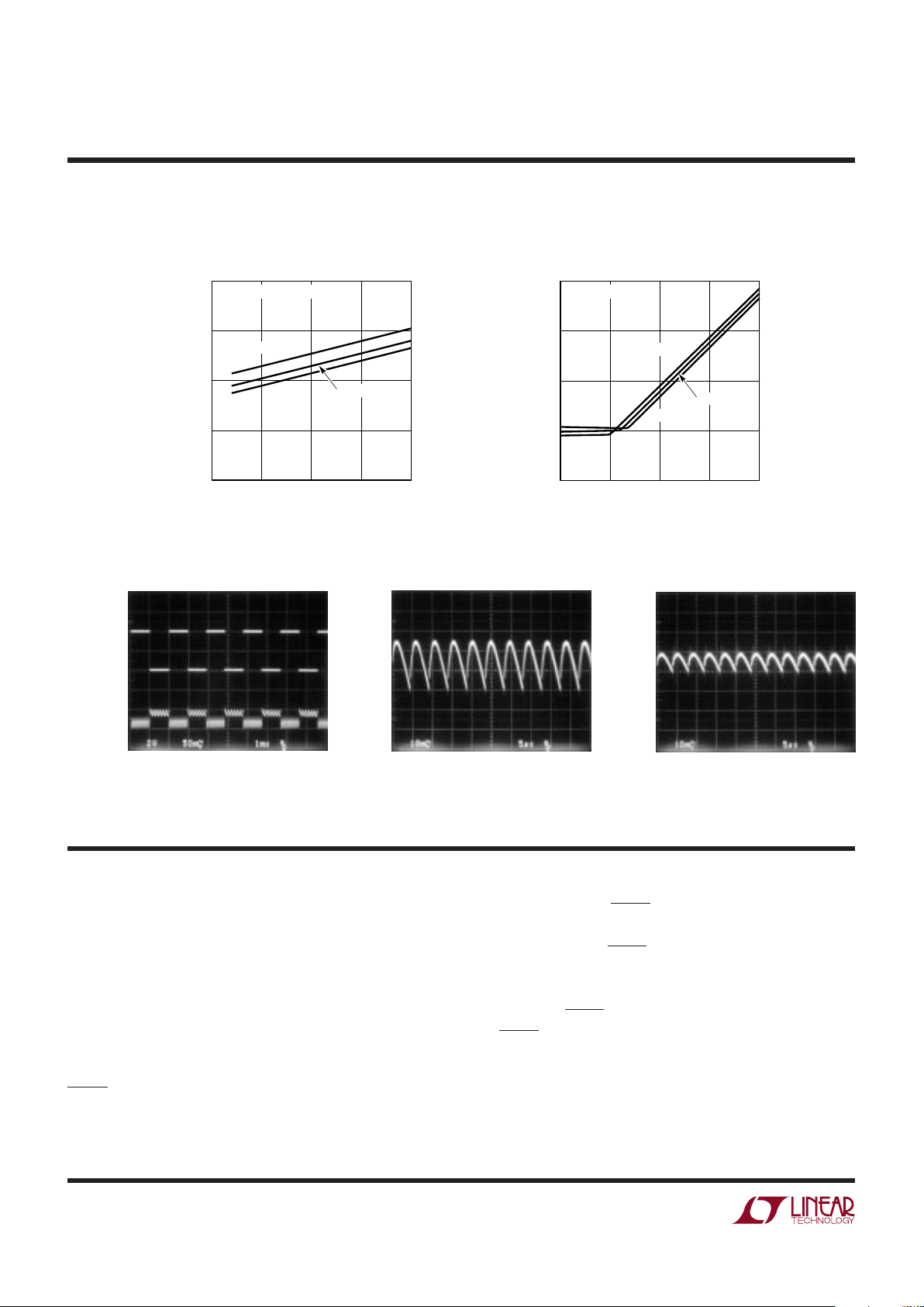
LTC1503-X Output Short-Circuit
Current vs Input Voltage
LTC1503-X Start-Up Time
vs Soft-Start Capacitor
INPUT VOLTAGE (V)
2
OUTPUT CURRENT (mA)
20
30
6
1503-1.8/2 G10
10
0
3
4
5
40
V
OUT
SHORTED TO GND
TA = –40°C
TA = 85°C
T
A
= 25°C
SOFT-START CAPACITOR (nF)
0.01
START-UP TIME (ms)
1
10
100
1503-1.8/2 G10
0.1
0.01
0.1
1
10
100
VIN = 3.6V
TA = –40°C
TA = 25°C
TA = 85°C
Output Load Transient Response
(LTC1503-1.8,1mA to 100mA Step)
I
OUT
50mA/DIV
V
OUT
50mV/DIV
AC COUPLED
100mA
1mA
1ms/DIV
1503-1.8/2 G12
Output Ripple, C
OUT
= 10µF
V
OUT
10mV/DIV
AC COUPLED
5µs/DIV
1503-1.8/2 G13
VIN = 3.6V
V
OUT
= 2V
I
OUT
= 100mA
C
OUT
= 10µF CERAMIC
Output Ripple, C
OUT
= 22µF
V
OUT
10mV/DIV
AC COUPLED
5µs/DIV
1503-1.8/2 G14
VIN = 3.6V
V
OUT
= 2V
I
OUT
= 100mA
C
OUT
= 22µF CERAMIC
V
OUT
(Pin 1): Regulated Output Voltage. V
OUT
is discon-
nected from VIN during shutdown. Bypass V
OUT
to ground
with a ≥10µF low ESR capacitor.
C1– (Pin 2): Flying Capacitor One Negative Terminal.
C1+ (Pin 3): Flying Capacitor One Positive Terminal.
VIN (Pin 4): Input Voltage. VIN may be between 2.4V and
6V. Bypass VIN to ground with a ≥10µF low ESR capacitor.
SHDN/SS (Pin 5): Shutdown/Soft-Start Control. The pin
is designed to be driven with an external open-drain
output. Holding the SHDN/SS pin below 0.25V will force
the part into shutdown mode. An internal pull-up current
of 2µA will force the SHDN/SS voltage to climb to VIN once
the device driving the pin is forced into a Hi-Z state. To
limit inrush current on start-up, connect a capacitor
between the SHDN/SS pin and ground. Capacitance on
the SHDN/SS pin will limit the dV/dt of the pin during turnon which, in turn, will limit the dV/dt of V
OUT
. By selecting
an appropriate soft-start capacitor for a known output
capacitor, the user can control the inrush current during
UU
U
PI FU CTIO S
 Loading...