

Linear Technology LTC1502-3.3 Datasheet
FEATURES
■
Input Voltage Range: 0.9V to 1.8V
■
0.9V Guaranteed Start-Up Voltage
■
Regulated Output Voltage: 3.3V ±4%
■
Output Current: 10mA (VIN ≥ 1V)
■
No Inductors
■
Shutdown Disconnects Load from V
■
Low Operating Current: 40µA
■
Low Shutdown Current: 5µA
■
Short-Circuit and Overtemperature Protected
■
Application Circuit Fits in <0.125in2 PCB Area
■
Available in 8-Pin MSOP and SO Packages
IN
U
APPLICATIO S
■
Pagers
■
Battery Backup Supplies
■
Portable Electronic Equipment
■
Handheld Medical Instruments
■
Glucose Meters
LTC1502-3.3
Single Cell to 3.3V
Regulated Charge Pump
DC/DC Converter
U
DESCRIPTIO
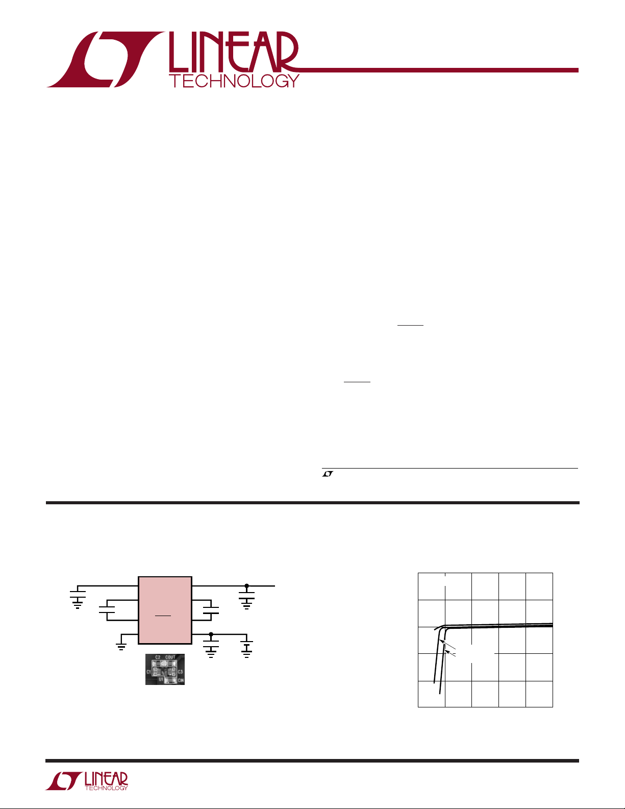
The LTC®1502-3.3 is a quadrupler charge pump DC/DC
converter that produces a regulated 3.3V output from a
single alkaline cell input. It requires only five small external
capacitors—no inductors are required. Low supply current (40µA typical, 5µA in shutdown) and minimal external
components make the LTC1502-3.3 ideal for space and
power conscious single-cell applications. The total printed
circuit board area of the circuit shown below is less than
0.125in2.
Forcing the C1–/SHDN pin low through an external resis-
tive pull-down puts the part into shutdown mode. During
shutdown, the internal oscillator is stopped and the load is
disconnected from VIN. An internal pull-up current on the
C1–/SHDN pin forces the part back into normal operation
once the pull-down resistance is removed.
The LTC1502-3.3 is short-circuit protected and survives
an indefinite V
available in 8-pin MSOP and SO packages.
, LTC and LT are registered trademarks of Linear Technology Corporation.
short to ground. The LTC1502-3.3 is
OUT
TYPICAL APPLICATIO
Single Cell to 3.3V DC/DC Converter
10µF
1
C2
2
C1
1µF
3
C1–/SHDN
4
GND
PCB LAYOUT FITS IN <0.125IN
V
+
LTC1502-3.3
OUT
C3
C3
+
–
V
IN
U
Output Voltage vs Input Voltage
3.5
8
7
1µF
6
5
10µF
2
V
OUT
I
OUT
10µF
V
IN
SINGLE CELL
NiCd or
ALKALINE
= 3.3V
= 10mA
1502-3.3 TA01
TA = 25°C
3.4
3.3
3.2
OUTPUT VOLTAGE (V)
3.1
3.0
0.8
1.0
I
= 10mA
OUT
= 15mA
I
OUT
1.4
1.2
INPUT VOLTAGE (V)
1.6
1502-3.3 TA02
1.8
1
LTC1502-3.3
1
2
3
4
8
7
6
5
TOP VIEW
V
OUT
C3
+
C3
–
V
IN
C2
C1
+
C1–/SHDN
GND
S8 PACKAGE
8-LEAD PLASTIC SO
WW
W
ABSOLUTE MAXIMUM RATINGS
U
(Note 1)
VIN to GND.................................................. –0.3V to 2V
V
to GND ............................................... – 0.3V to 5V
OUT
All Other Pins to GND ................................. –0.3V to 5V
V
Short-Circuit Duration............................ Indefinite
OUT
Storage Temperature Range ................ –65°C to 150°C
U
W
PACKAGE/ORDER INFORMATION
ORDER PART
TOP VIEW
C2
+
C1
C1–/SHDN
GND
8-LEAD PLASTIC MSOP
T
JMAX
1
2
3
4
MS8 PACKAGE
= 125°C, θJA = 250°C/ W
8
V
OUT
+
7
C3
–
6
C3
5
V
IN
Consult factory for Military grade parts.
NUMBER
LTC1502CMS8-3.3
MS8 PART MARKING
LTEC
Operating Temperature Range
Commercial ............................................ 0°C to 70°C
Extended Commercial (Note 4).......... –40°C to 85°C
Industrial ........................................... –40°C to 85°C
Lead Temperature (Soldering, 10 sec)................. 300°C
U
ORDER PART
NUMBER
LTC1502CS8-3.3
LTC1502IS8-3.3
S8 PART MARKING
150233
T
= 125°C, θJA = 150°C/ W
JMAX
502I33
ELECTRICAL CHARACTERISTICS
The ● denotes the specifications which apply over the full operating temperature range, otherwise specifications are at TA = 25°C.
VIN = 0.9V to 1.8V, C1 = C3 = 1µF, CIN = C2 = C
PARAMETER CONDITIONS MIN TYP MAX UNITS
VIN Operating Voltage ● 0.9 1.8 V
Minimum VIN Start-Up Voltage TA = 0°C to 70°C (Note 2) ● 0.75 0.9 V
V
Voltage I
OUT
VIN Operating Current I
VIN Shutdown Current C1–/SHDN = 0V ● 515 µA
Output Ripple I
Efficiency VIN = 1V, I
Switching Frequency Oscillator Free-Running 500 kHz
C1–/SHDN Shutdown Input Threshold C1–/SHDN in Hi-Z Sampling State ● 0.20 0.55 0.85 V
C1–/SHDN Shutdown Input Current C1–/SHDN = 0V (Note 3) ● –0.5 –2.5 – 8 µA
V
Turn-On Time VIN = 1V, I
OUT
V
Short-Circuit Current VIN = 1.5V, V
OUT
Note 1: Absolute Maximum Ratings are those values beyond which the life
of the device may be impaired.
Note 2: Start-up testing is done with a 100kΩ equivalent load on V
Note 3: Currents flowing into the device are positive polarity. Currents
flowing out of the device are negative polarity.
2
= 10µF unless otherwise specified.
OUT
T
= –40°C to 85°C (Note 2) ● 1.1 V
A
≤ 3.5mA, 0.9V ≤ VIN ≤ 1.8V ● 3.17 3.3 3.43 V
OUT
≤ 10mA, 1V ≤ VIN ≤ 1.8V ● 3.17 3.3 3.43 V
I
OUT
= 0mA ● 40 90 µA
OUT
= 10mA, VIN = 1.25V 50 mV
OUT
= 10mA 77 %
OUT
= 0mA 5 ms
OUT
Forced to 0V 20 mA
OUT
Note 4: Commercial grade specifications are guaranteed over the 0°C to
70°C operating temperature range. In addition, commercial grade
OUT
.
specifications are assured over the –40°C to 85°C operating temperature
range by design, characterization and correlation with statistical process
controls. Industrial grade specifications are guaranteed and tested over the
–40°C to 85°C operating temperature range.
P-P
UW
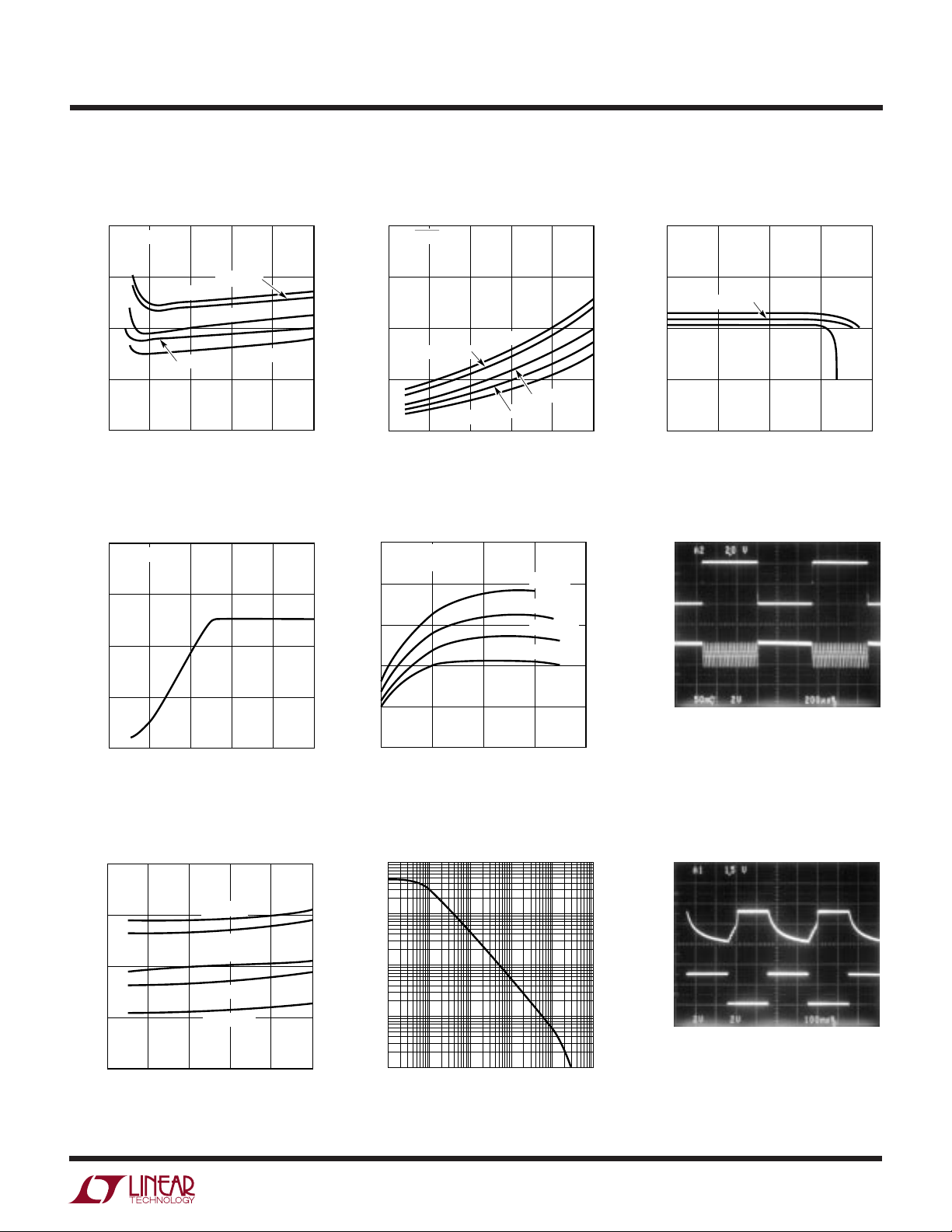
TYPICAL PERFOR A CE CHARACTERISTICS
LTC1502-3.3
No Load Input Current
vs Input Voltage
80
I
= 0mA
OUT
60
40
INPUT CURRENT (µA)
20
0
0.8
TA = 85°C
TA = 0°C
1.0
INPUT VOLTAGE (V)
1.2
= 70°C
T
A
TA = 25°C
T
1.4
Maximum Start-Up Load Current
vs Input Voltage
16
TA = 25°C
12
8
LOAD CURRENT (mA)
4
0
0.8
1.0
INPUT VOLTAGE (V)
1.2
1.4
= –40°C
A
1.6
1.6
1502-3.3 G01
1502-3.3 G04
1.8
1.8
Shutdown Input Current
vs Input Voltage
16
–
/SHDN = 0V
C1
12
8
TA = 70°C
INPUT CURRENT (µA)
4
0
1.0
0.8
T
T
= – 40°C
A
1.2
INPUT VOLTAGE (V)
Efficiency vs Output Current
100
TA = 25°C
= 3.3V
V
OUT
80
60
40
EFFICIENCY (%)
20
0
0.01
0.1
OUTPUT CURRENT (mA)
1
= 85°C
A
1.4
T
A
TA = 25°C
= 0°C
1.6
= 1V
V
IN
VIN = 1.25V
VIN = 1.5V
VIN = 1.8V
10
1502-3.3 G05
1502-3.3 G02
100
1.8
Output Voltage vs Output Current
3.40
3.35
3.30
OUTPUT VOLTAGE (V)
3.25
3.20
0.01
I
OUT
0mA to 10mA
5mA/DIV
V
OUT
AC COUPLED
50mV/DIV
= 25°C
T
A
VIN = 1.5V
V
= 1V
IN
0.1
OUTPUT CURRENT (mA)
= 1.8V
V
IN
1
10
Load Transient Response
VIN = 1.25V
T
= 25°C
A
200µs/DIV
100
1502-3.3 G03
1502-3.3 G06
Oscillator Frequency
vs Input Voltage
700
600
500
400
OSCILLATOR FREQUENCY (kHz)
300
0.8
1.0
TA = 85°C
TA = – 40°C
1.2
INPUT VOLTAGE (V)
TA = 70°C
TA = 25°C
TA = 0°C
1.4
1.6
1502-3.3 G07
1.8
Calculated Battery Life,
Battery = 2400mA • Hr AA Cell
100k
10k
1k
BATTERY LIFE (HOURS)
100
10
0.001
0.1 1 100.01 100
AVERAGE LOAD CURRENT (mA)
1502-3.3 G08
Shutdown Waveforms
(See Figure 1)
V
OUT
2V/DIV
OFF
V
CTRL
ON
V
= 1.25V
IN
R
= 10k
LOAD
= 25°C
T
A
100µs/DIV
1502-3.3 G09
3
 Loading...