

Linear Technology LTC1482 Datasheet
FEATURES
LTC1482
Low Power RS485 Transceiver
with Carrier Detect and
Receiver Fail-Safe
U
DESCRIPTIO
■
No Damage or Latchup to ±15kV (Human Body
Model), IEC1000-4-2 Level 4 (±8kV) Contact and
Level 3 (±8kV) Air Discharge
■
Active Low Carrier Detect Output
■
Guaranteed High Receiver Output State for
Floating, Shorted or Terminated Inputs with
No Signal Present
■
Drives Low Cost Residential Telephone Wires
■
Low Power: ICC = 700µA Max with Driver Disabled
■
ICC = 900µA Max in Driver Mode Without Load
■
20µA Max Quiescent Current in Shutdown Mode
■
Single 5V Supply
■
–7V to 12V Common Mode Range Permits ±7V
Ground Difference Between Devices on the Data Line
■
Maximum Data Rate of 4Mbps
■
Power Up/Down Glitch-Free Driver Outputs
■
Up to 32 Transceivers on the Bus
■
Available in 8-Lead MSOP, PDIP and SO Packages
U
APPLICATIO S
■
Battery-Powered RS485/RS422 Applications
■
Low Power RS485/RS422 Transceiver
■
Level Translator
, LTC and LT are registered trademarks of Linear Technology Corporation.
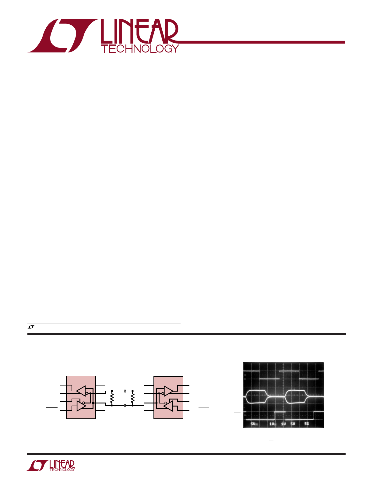
The LTC®1482 is a low power RS485 compatible transceiver that offers an active low carrier detect output. The
open-drain carrier detect pin allows several transceivers
to share the same carrier detect line and can be used to
detect the insertion or removal of a driven RS485/RS422
cable.
Enhanced ESD protection allows the LTC1482 to withstand ±15kV (human body model), IEC-1000-4-2 level 4
(±8kV) contact and level 3 (±8kV) air discharge ESD
without latchup or damage.
The LTC1482 receiver stays alive at all times except in
shutdown. The supply current is a maximum of 700µA
and 900µA when the driver is disabled and enabled
respectively. In shutdown, the quiescent current of the
LTC1482 drops to a maximum of 20µA.
When the driver is disabled or the LTC1482 is in shutdown, the driver outputs are three-stated and remain in
a high impedance state over the RS485 common mode
range.
Excessive power dissipation caused by bus contention or
faults is prevented by a thermal shutdown circuit, which
forces the driver outputs into a high impedance state.
The LTC1482 is fully specified over the commercial and
industrial temperature ranges and is available in 8-lead
MSOP, PDIP and SO packages.
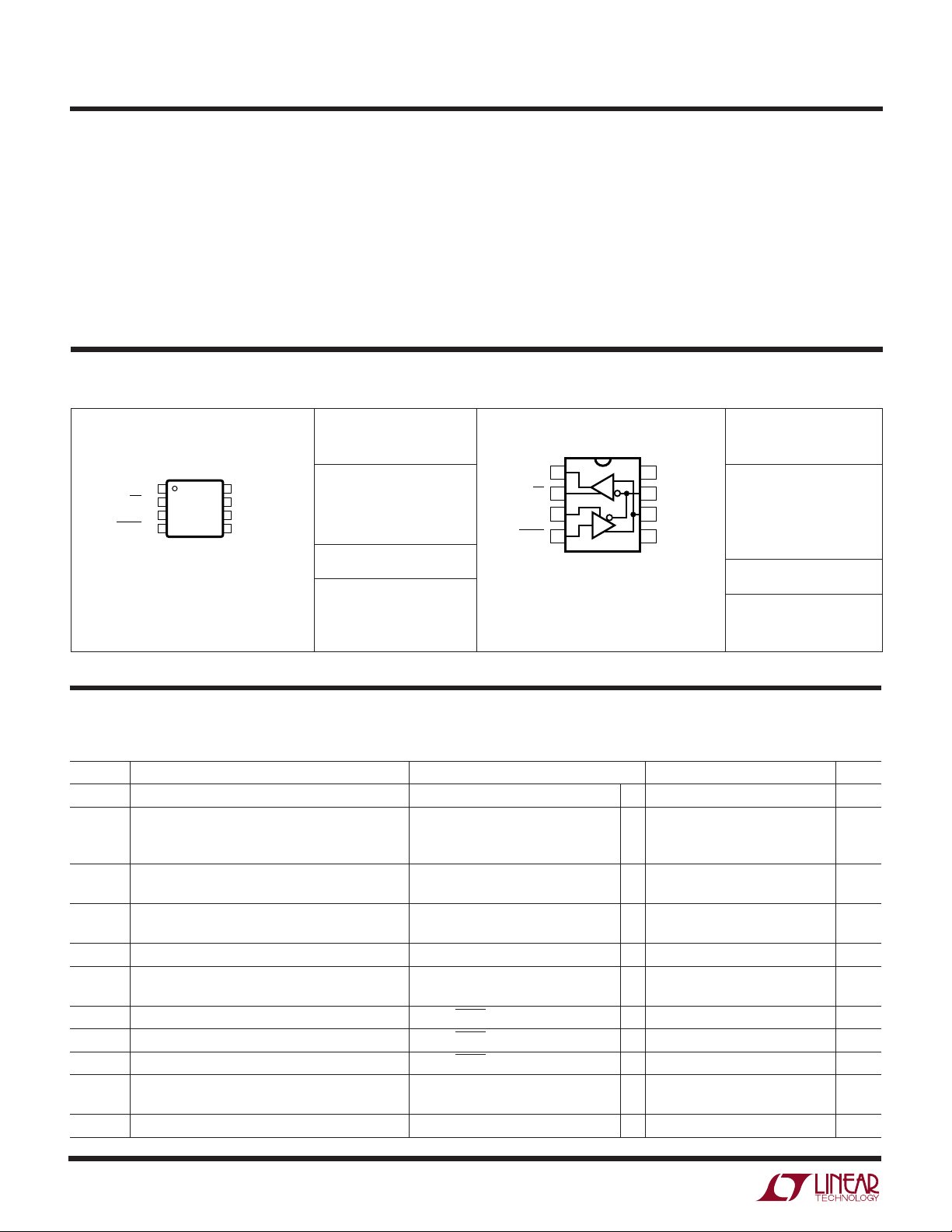
TYPICAL APPLICATIO
RS485 Interface
RO1
CD1
DE1
DI1/SHDN1
LTC1482
R
D
B1
A1
V
CC1
120Ω 120Ω
GND1
U
V
CC2
GND2
Carrier Detect Output (2000 Foot STP Cable)
LTC1482
B2
A2
R
D
RO2
CD2
DE2
DI2/SHDN2
1482 TA01
DE1
A2
B2
CD2
DE1 ↑↓ Dl1 = V
DE2 = 0 Dl2 = V
1k PULL-UP AT CD
CC
CC
1482 TA01a
1
LTC1482
WW
W
U
ABSOLUTE MAXIMUM RATINGS
(Note 1)
Supply Voltage (VCC)............................................... 6.5V
Control Input Voltages ................. –0.3V to (VCC + 0.3V)
Carrier Detect Voltage ................................. –0.3V to 8V
Driver Input Voltage ..................... –0.3V to (VCC + 0.3V)
Driver Output Voltages ................................. –7V to 10V
Receiver Input Voltages (Driver Disabled) .. –12V to 14V
Receiver Output Voltage ............... – 0.3V to (VCC + 0.3V)
U
W
U
PACKAGE/ORDER INFORMATION
ORDER PART
NUMBER
RO
1
CD
2
DE
3
DI/SHDN
4
8-LEAD PLASTIC MSOP
T
= 125°C, θJA = 200°C/ W
JMAX
TOP VIEW
MS8 PACKAGE
8
V
CC
7
B
6
A
5
GND
LTC1482CMS8 LTC1482CN8
MS8 PART MARKING
LTCB
Junction Temperature .......................................... 125°C
Operating Temperature Range
LTC1482C ........................................ 0°C ≤ TA ≤ 70°C
LTC1482I...................................... –40°C ≤ TA ≤ 85°C
Storage Temperature Range .................. –65°C to 150°C
Lead Temperature (Soldering, 10 sec)...................300°C
ORDER PART
RO
1
CD
2
DE
3
DI/SHDN
4
N8 PACKAGE
8-LEAD PDIP
T
= 125°C, θJA = 130°C/ W (N8)
JMAX
T
= 125°C, θJA = 135°C/W (S8)
JMAX
TOP VIEW
8-LEAD PLASTIC SO
V
8
CC
B
7
A
6
GND
5
S8 PACKAGE
NUMBER
LTC1482CS8
LTC1482IN8
LTC1482IS8
S8 PART MARKING
1482
1482I
Consult factory for Military grade parts.
ELECTRICAL CHARACTERISTICS
temperature range, otherwise specifications are at T
SYMBOL PARAMETER CONDITIONS MIN TYP MAX UNITS
V
OD1
V
OD2
V
OD3
∆V
OD
V
OC
∆|VOC| Change in Magnitude of Driver Common Mode R = 22Ω, 27Ω or R = 50Ω, Figure 1 ● 0.2 V
V
IH
V
IL
I
IN1
I
IN2
V
THRO
Differential Driver Output Voltage (Unloaded) I
Differential Driver Output Voltage (with Load) R = 50Ω (RS422) ● 2V
Differential Driver Output Voltage V
(with Common Mode)
Change in Magnitude of Driver Differential R = 22Ω, 27Ω or R = 50Ω, Figure 1 ● 0.2 V
Output Voltage for Complementary Output States V
Driver Common Mode Output Voltage R = 22Ω, 27Ω or R = 50Ω, Figure 1 ● 3V
Output Voltage for Complementary Output States
Input High Voltage DE, DI/SHDN ● 2V
Input Low Voltage DE, DI/SHDN ● 0.8 V
Input Current DE, DI/SHDN ● ±2 µA
Input Current (A, B) with Driver Disabled DE = 0, VCC = 0 or 5V, VIN = 12V ● 1.0 mA
Differential Input Threshold Voltage for Receiver –7V ≤ VCM ≤ 12V, DE = 0 ● –0.20 –0.015 V
The ● denotes the specifications which apply over the full operating
= 25°C. VCC = 5V ±5% (Notes 2 and 3) unless otherwise noted.
A
= 0 ● V
OUT
R = 27Ω (RS485) Figure 1
R = 22Ω, Figure 1
= –7V to 12V, Figure 2 ● 1.5 5 V
TST
= –7V to 12V, Figure 2
TST
DE = 0, V
= 0 or 5V, VIN = –7V ● –0.8 mA
CC
● 1.5 5 V
● 1.5 5 V
CC
V
2
LTC1482
ELECTRICAL CHARACTERISTICS
temperature range, otherwise specifications are at T
The ● denotes the specifications which apply over the full operating
= 25°C. VCC = 5V ±5% (Notes 2 and 3) unless otherwise noted.
A
SYMBOL PARAMETER CONDITIONS MIN TYP MAX UNITS
V
∆V
V
V
I
OZR
THCD
TH
OH
OL
Differential Input Threshold Voltage for CD = 1 –7V ≤ VCM ≤ 12V, DE = 0 ● –0.20 0.20 V
Receiver Input Hysteresis VCM = 0V, DE = 0 ±30 mV
CD Output High Voltage I
RO Output High Voltage I
RO and CD Output Low Voltage I
Three-State (High Impedance) Receiver Output VCC = Max, 0.4V ≤ V
= –10µA, (VA – VB) = 0V ● 3.4 V
OUT
= –4mA, (VA – VB) = 200mV ● 3.5 V
OUT
= 4mA, (VA – VB) = –200mV ● 0.4 V
OUT
≤ 2.4V ● ±1 µA
OUT
Current in Shutdown DI/SHDN = 0, DE = 0
R
IN
I
CC
I
SHDN
I
OSD1
I
OSD2
I
OS
I
PULL-UP
Receiver Input Resistance –7V ≤ VCM ≤ 12V ● 12 22 kΩ
Supply Current No Load, Driver Enabled (DE = VCC) ● 580 900 µA
No Load, Driver Disabled (DE = 0)
● 430 700 µA
Supply Current in Shutdown Mode DE = 0, DI = 0 ● 10 20 µA
Driver Short-Circuit Current, V
Driver Short-Circuit Current, V
RO and CD Short-Circuit Current 0V ≤ V
= High (Note 4) –7V ≤ V
OUT
= Low (Note 4) –7V ≤ V
OUT
≤ 10V 35 250 mA
OUT
≤ 10V 35 250 mA
OUT
OUT
≤ V
CC
● 785mA
CD Pull-Up Current CD = 0V ● 15 30 60 µA
U
SWITCHING CHARACTERISTICS
temperature range, otherwise specifications are at T
The ● denotes the specifications which apply over the full operating
= 25°C. VCC = 5V ±5% (Notes 2 and 3) unless otherwise noted.
A
SYMBOL PARAMETER CONDITIONS MIN TYP MAX UNITS
t
PLH
t
PHL
t
SKEW
tr, t
f
t
ZH
t
ZL
t
LZ
t
HZ
t
ZH(SHDN)
Driver Input to Output R
= 54Ω, CL1 = CL2 = 100pF ● 10 28 60 ns
DIFF
Driver Input to Output (Figures 4, 6) ● 10 30 60 ns
Driver Output to Output ● 210 ns
Driver Rise or Fall Time ● 31540 ns
Driver Enable to Output High CL = 100pF (Figures 5, 7) S2 Closed ● 40 70 ns
Driver Enable to Output Low CL = 100pF (Figures 5, 7) S1 Closed ● 40 100 ns
Driver Disable Time from Low CL = 15pF (Figures 5, 7) S1 Closed ● 40 70 ns
Driver Disable Time from High CL = 15pF (Figures 5, 7) S2 Closed ● 40 70 ns
Driver Enable from Shutdown to Output High CL = 100pF (Figures 5, 7) S2 Closed ● 40 100 ns
(Note 5)
t
ZL(SHDN)
t
HZ(SHDN)
t
LZ(SHDN)
f
MAX
t
PLH
Driver Enable from Shutdown to Output Low CL = 100pF (Figures 5, 7) S1 Closed ● 40 100 ns
Driver Disable on Shutdown from Output High CL = 15pF (Figures 5, 7) S2 Closed ● 40 100 ns
Driver Disable on Shutdown from Output Low CL = 15pF (Figures 5, 7) S1 Closed ● 40 100 ns
Maximum Data Rate (Note 6) ● 4 5 Mbps
Receiver Input to Output (Note 7) R
= 54Ω, CL1 = CL2 = 100pF, ● 30 138 200 ns
DIFF
(Figures 4, 8)
t
PHL
Receiver Input to Output R
= 54Ω, CL1 = CL2 = 100pF, ● 30 122 200 ns
DIFF
(Figures 4, 8)
t
SKD
|t
– t
PLH
| Differential Receiver Skew R
PHL
= 54Ω, CL1 = CL2 = 100pF, 16 ns
DIFF
(Figures 4, 8)
t
t
CDH
CDL
Receiver Input to CD Output High (Note 7) R
Receiver Input to CD Output Low (Note 7) R
= 54Ω, CL1 = CL2 = 100pF, ● 2900 5000 ns
DIFF
(Figures 4, 10) DI/SHDN = V
= 54Ω, CL1 = CL2 = 100pF, ● 150 300 ns
DIFF
(Figures 4, 10) DI/SHDN = V
CC
CC
3

LTC1482
U
SWITCHING CHARACTERISTICS
temperature range, otherwise specifications are at T
SYMBOL PARAMETER CONDITIONS MIN TYP MAX UNITS
t
CDH(SHDN)
t
CDL(SHDN)
t
ZH(SHDN)
t
ZL(SHDN)
t
HZ(SHDN)
t
LZ(SHDN)
Receiver Input to CD Output High at Shutdown R
Receiver Input to CD Output Low from Shutdown R
Receiver Enable from Shutdown to Output High CL = 15pF (Figures 3, 9) S2 Closed, ● 30 600 ns
Receiver Enable from Shutdown to Output Low CL = 15pF (Figures 3, 9) S1 Closed, ● 2600 5000 ns
Receiver Disable from High on Shutdown CL = 15pF (Figures 3, 9) S2 Closed, ● 200 600 ns
Receiver Disable from Low on Shutdown CL = 15pF (Figures 3, 9) S1 Closed, ● 200 600 ns
The ● denotes the specifications which apply over the full operating
= 25°C. VCC = 5V ±5% (Notes 2 and 3) unless otherwise noted.
A
= 54Ω, CL1 = CL2 = 100pF, ● 2600 5000 ns
DIFF
(Figures 4, 11) DI/SHDN = DE
= 54Ω, CL1 = CL2 = 100pF, ● 2600 5000 ns
DIFF
(Figures 4, 11) DI/SHDN = DE
A = 750mV, B = –750mV, DE = 0,
DI/SHDN =
A = –750mV, B = 750mV, DE = 0,
DI/SHDN =
A = 750mV, B = –750mV, DE = 0,
DI/SHDN =
A = –750mV, B = 750mV, DE = 0,
DI/SHDN =
Note 1: Absolute Maximum Ratings are those values beyond which the life of
a device may be impaired.
Note 2: All typicals are given for V
= 5V and TA = 25°C.
CC
Note 3: All currents into device pins are positive; all currents out of device
pins are negative. All voltages are referenced to device ground unless
otherwise specified.
Note 4: For higher ambient temperatures, the part may enter thermal
shutdown during short-circuit conditions.
Note 5: Both driver input and driver enable pins are pulled high
simultaneously.
Note 6: Guaranteed by design.
Note 7: Measured with an external LTC1485 driver.
UW
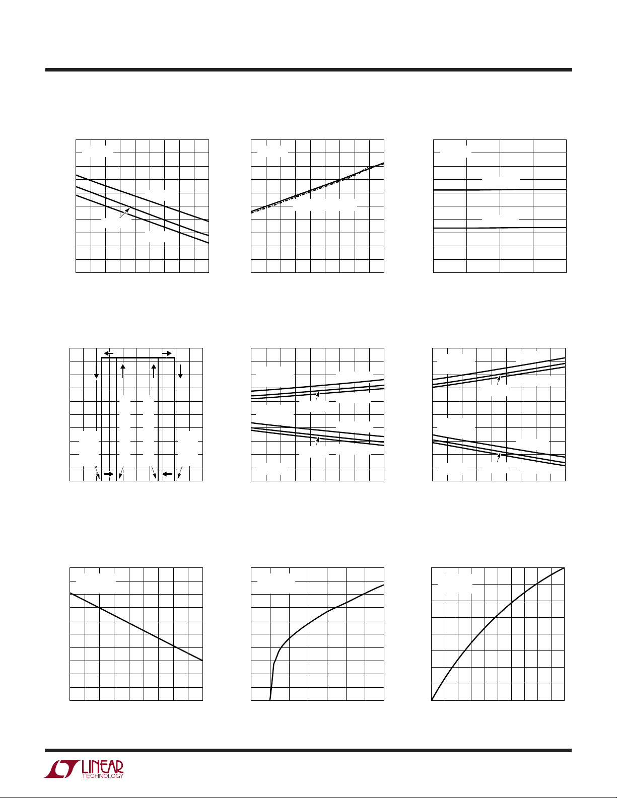
TYPICAL PERFOR A CE CHARACTERISTICS
Receiver Output Voltage vs Input
Voltage
6
TA = 25°C
5
4
3
2
1
RECEIVER OUTPUT VOLTAGE (V)
V
THRO(LOW)
0
–0.16 –0.12 –0.08 –0.04 0
–0.2
INPUT VOLTAGE (V)
V
THRO(HIGH)
1482 G01
Receiver Input Threshold Voltage
(Output High) vs Temperature
0
–0.02
–0.04
–0.06
–0.08
–0.1
–0.12
–0.14
–0.16
–0.18
RECEIVER INPUT THRESHOLD VOLTAGE (mV)
–0.20
–55 –35 –15 5 25 45 65 85 105 125
VCM = 12V
VCM = 0V
TEMPERATURE (°C)
VCC = 5V
V
VCM = –7V
THRO(HIGH)
1482 G02
Receiver Input Threshold Voltage
(Output Low) vs Temperature
0
–0.02
–0.04
–0.06
–0.08
–0.1
–0.12
–0.14
–0.16
–0.18
RECEIVER INPUT THRESHOLD VOLTAGE (mV)
–0.20
–55 –35 –15 5 25 45 65 85 105 125
VCM = 12V
VCM = 0V
TEMPERATURE (°C)
VCC = 5V
V
VCM = –7V
THRO(LOW)
1482 G03
4
UW
TEMPERATURE (°C)
CARRIER DETECT THRESHOLD VOLTAGE (V)
1482 G09
0.25
0.20
0.15
0.10
0.05
0
–0.05
–0.10
–0.15
–0.20
–0.25
VCC = 5V
POSITIVE
V
THCD(LOW)
NEGATIVE
V
THCD(LOW)
–55 –35 –15 5 25 45 65 85 105 125
VCM = 12V
VCM = –7V
VCM = 12V
VCM = –7V
VCM = 0V
VCM = 0V
TYPICAL PERFOR A CE CHARACTERISTICS
LTC1482
Receiver Input Offset Voltage vs
Temperature
0
VCC = 5V
–20
–40
–60
–80
–100
–120
–140
–160
–180
RECEIVER INPUT OFFSET VOLTAGE (mV)
–200
–55 –35 –15 5 25 45 65 85 105 125
VCM = 0V
TEMPERATURE (°C)
VCM = 12V
VCM = –7V
Carrier Detect Output Voltage vs
Receiver Input Voltage
5.0
4.5
4.0
3.5
3.0
2.5
2.0
1.5
1.0
0.5
CARRIER DETECT OUTPUT VOLTAGE (V)
0
–0.25
THCD(LOW)
NEGATIVE
V
–0.15 –0.05 0.05 0.15 0.25
RECEIVER INPUT VOLTAGE (V)
THCD(HIGH)
THCD(HIGH)
NEGATIVE, V
POSITIVE, V
1482 G04
THCD(LOW)
POSITIVE
V
1482 G07
Receiver Hysteresis vs
Temperature
100
VCC = 5V
90
80
70
60
50
40
HYSTERESIS (mV)
30
20
10
0
–55 –35 –15 5 25 45 65 85 105 125
VCM = –7V TO 12V
TEMPERATURE (°C)
Carrier Detect Threshold Voltage
(Output High) vs Temperature
0.25
0.20
POSITIVE
0.15
V
THCD(HIGH)
0.10
0.05
NEGATIVE
0
V
–0.05
–0.10
–0.15
–0.20
CARRIER DETECT THRESHOLD VOLTAGE (V)
–0.25
THCD(HIGH)
VCC = 5V
–55 –35 –15 5 25 45 65 85 105 125
VCM = 0V
VCM = 0V
TEMPERATURE (°C)
VCM = 12V
VCM = –7V
VCM = 12V
VCM = –7V
1482 G05
1482 G08
Receiver Input Threshold Voltage
vs Supply Voltage
0
TA = 25°C
–0.02
–0.04
–0.06
–0.08
–0.10
–0.12
–0.14
–0.16
–0.18
RECEIVER INPUT THRESHOLD VOLTAGE (V)
–0.20
4.5
V
THRO(HIGH)
V
THRO(LOW)
4.75 5 5.25 5.5
SUPPLY VOLTAGE (V)
Carrier Detect Threshold Voltage
(Output Low) vs Temperature
1482 G06
Receiver Output High Voltage vs
Temperature
4.5
VCC = 4.75V
4.4
4.3
4.2
4.1
4.0
3.9
3.8
3.7
RECEIVER OUTPUT HIGH VOLTAGE (V)
3.6
3.5
= –8mA
I
OUT
–55 –35 –15 5 25 45 65 85 105 125
TEMPERATURE (°C)
1482 G10
Carrier Detect Output High
Voltage vs Output Current
5.0
VCC = 4.75V
4.5
= 25°C
T
A
4.0
3.5
3.0
2.5
2.0
1.5
1.0
0.5
CARRIER DETECT OUTPUT HIGH VOLTAGE (V)
0
–35 –30 –25 –20 –15 –10 –5 0
OUTPUT CURRENT (µA)
1482 G11
Receiver and Carrier Detect
Output Low Voltage vs Output
Current
40
TA = 25°C
35
= 4.75
V
CC
30
25
20
15
OUTPUT CURRENT (mA)
10
5
0
0
0.2 0.4 0.6 0.8 1 1.2 1.4 1.6 1.8 2
OUTPUT LOW VOLTAGE (V)
1482 G12
5
 Loading...