

Linear Technology LTC1477, LTC1478 Datasheet
FEATURES
■
Extremely Low R
■
No Parasitic Body Diode
■
Built-In Short-Circuit Protection: 2A
■
Built-In Thermal Overload Protection
■
Operates from 2.7V to 5.5V
■
Inrush Current Limited
■
Ultralow Standby Current: 0.01µA
■
Built-In Charge Pump
■
Controlled Rise and Fall Times: tR = 1ms
■
Single Switch in 8-Pin SO Package
■
Dual Switch in Narrow 16-Pin SO Package
Switch: 0.07
DS(ON)
U
APPLICATIONS
■
Notebook Computer Power Management
■
Power Supply/Load Protection
■
Supply/Battery Switch-Over Circuits
■
Circuit Breaker Function
■
"Hot Swap" Board Protection
■
Peripheral Power Protection
Ω
LTC1477/LTC1478
Single and Dual Protected
High Side Switches
U
DESCRIPTION
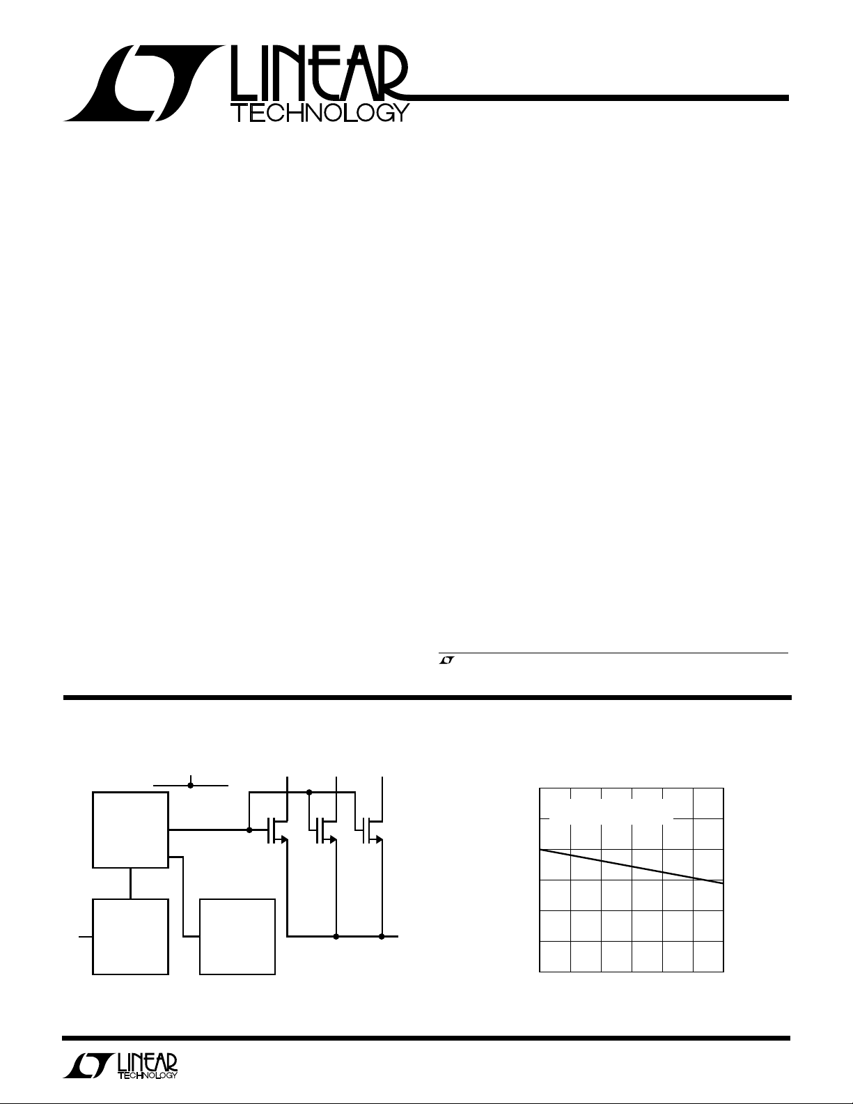
The LTC®1477/LTC1478 protected high side switches
provide extremely low R
DS(ON)
protection against short-circuit and thermal overload conditions. A built-in charge pump generates gate drive
higher than the supply voltage to fully enhance the internal
NMOS switch. This switch has no parasitic body diode and
therefore no current flows through the switch when it is
turned off and the output is forced above the input supply
voltage. (DMOS switches have parasitic body diodes that
become forward biased under these conditions.)
Two levels of protection are provided by the
LTC1477/LTC1478. The first level of protection is shortcircuit current limit which is set at 2A. The short-circuit
current can be reduced to as low as 0.85A by disconnecting portions of the power device (see Applications Information). The second level of protection is provided by
thermal overload protection which limits the die temperature to approximately 130°C.
The LTC1477 single is available in 8-lead SO packaging.
The LTC1478 dual is available in 16-lead SO packaging.
switching with built-in
SI PLIFIED BLOCK DIAGRAM
EN
GATE CHARGE
AND
DISCHARGE
CONTROL LOGIC
CHARGE
PUMP
*NMOS SWITCHES WITH NO PARASITIC BODY DIODES
V
INS
CURRENT LIMIT
AND THERMAL
SHUTDOWN
V
IN1
***
V
IN2
, LTC and LT are registered trademarks of Linear Technology Corporation.
WW
V
IN3
V
OUT
LTC1477/1478 • TA01
5.20
5.10
5.00
4.90
4.80
OUTPUT VOLTAGE (V)
4.70
4.60
Switch Output Voltage
TA = 25°C
= V
V
0
= V
IN1
IN2
0.5 0.75 1.00
0.25
OUTPUT CURRENT (A)
IN3
= V
INS
= 5V
1.25 1.50
LTC1477/1478 • TP02
1
LTC1477/LTC1478
WW
W
U
ABSOLUTE MAXIMUM RATINGS
Supply Voltage .......................................................... 7V
Enable Input Voltage...................... (7V) to (GND –0.3V)
Output Voltage (OFF) (Note 1) .......(7V) to (GND –0.3V)
Output Short-Circuit Duration.......................... Indefinite
Junction Temperature...........................................110°C
U
W
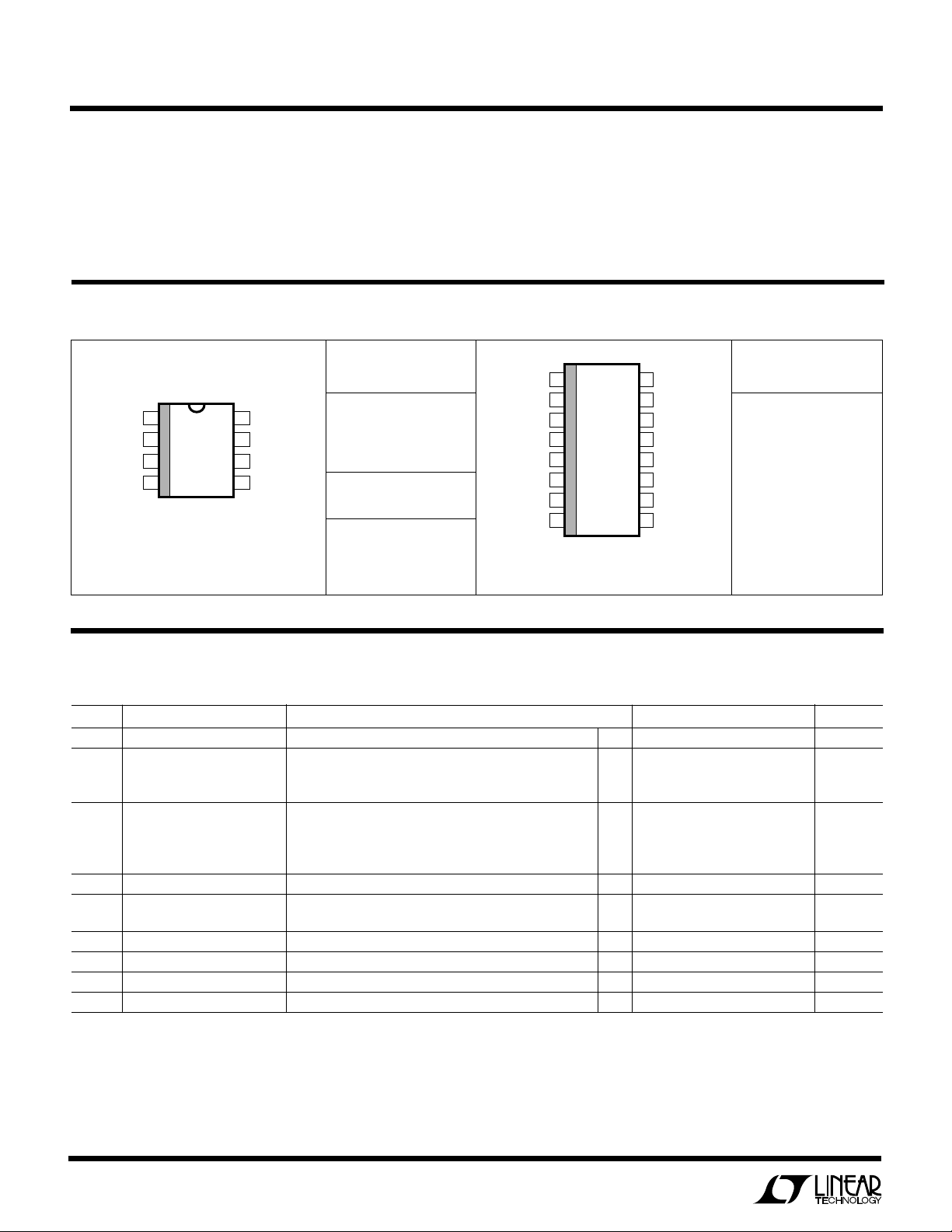
PACKAGE/ORDER INFORMATION
ORDER PART
NUMBER
LTC1477CS8
S8 PART MARKING
1477
V
1
OUT
V
2
IN1
V
3
INS
EN
4
8-LEAD PLASTIC SO
T
= 110°C, θJA = 120°C/W
JMAX
TOP VIEW
S8 PACKAGE
V
8
OUT
V
7
IN2
V
6
IN3
GND
5
Operating Temperature
LTC1477C/LTC1478C ..............................0°C to 70°C
Storage Temperature Range ................. –65°C to 150°C
Lead Temperature (Soldering, 10 sec)..................300°C
U
1
AV
OUT
2
AV
IN
3
AV
INS
4
AEN
5
GND
6
BV
IN3
7
BV
IN2
8
BV
OUT
16-LEAD PLASTIC SO
T
JMAX
TOP VIEW
16
15
14
13
12
11
10
9
S PACKAGE
= 110°C, θJA = 100°C/ W
AV
AV
AV
GND
BEN
BV
BV
BV
OUT
IN2
IN3
INS
IN1
OUT
ORDER PART
NUMBER
LTC1478CS
Consult factory for Industrial and Military grade parts.
ELECTRICAL CHARACTERISTICS
V
= V
= V
= V
INS
IN1
IN2
SYMBOL PARAMETER CONDITIONS MIN TYP MAX UNITS
V
IN
I
VIN
R
ON
I
LKG
I
SC
V
ENH
V
ENL
I
EN
t
D+R
The
Supply Voltage Range 2.7 5.5 V
Supply Current Switch OFF, Enable = 0V ● 0.01 10 µA
ON Resistance V
Output Leakage Current OFF Switch OFF, Enable = 0V ● ±20 µA
Short-Circuit Current Limit V
Enable Input High Voltage 3.0V ≤ V
Enable Input Low Voltage 3.0V ≤ V
Enable Input Current 0V ≤ VEN ≤ 5.5V ● ±1 µA
Delay and Rise Time R
● denotes specifications which apply over the full operating
temperature range.
Note 1: The V
Note 2: The V
pins are typically connected to V
V
IN3
pins must be connected together.
OUT
and V
INS
selectively disconnected to reduce the short-circuit current limit and
= 5V (Note 2), TA = 25°C, unless otherwise noted. Each channel of the LTC1478 is tested separately (Note 3).
IN3
Switch ON, Enable = 5V, VIN = 5V ● 120 180 µA
Switch ON, Enable = 3.3V, VIN = 3.3V ● 80 120 µA
= V
= V
= V
INS
V
INS
V
INS
V
INS
INS
V
INS
OUT
IN1
= V
= V
= V
= V
= V
IN2
= V
IN1
IN2
= 5V, V
IN1
= 3.3V, V
IN1
= V
IN1
IN2
= 5V, V
IN1
≤ 5.5V ● 2.0 V
INS
≤ 5.5V ● 0.8 V
INS
= 100Ω, C
= 5V, I
IN3
= V
= 3.3V, I
IN3
= V
IN2
IN3
= V
IN2
= V
= 5V, V
IN3
= V
IN2
IN3
= 1µF, to 90% of Final Value 0.50 1.00 2.00 ms
OUT
= 1A 0.07 0.12 Ω
OUT
= 1A 0.08 0.12 Ω
OUT
= NC, I
= NC, I
IN3
= NC, V
= 0.5A 0.12 0.20 Ω
OUT
= 0.5A 0.13 0.20 Ω
OUT
= 0V, (Note 4) 1.60 2.00 2.40 A
OUT
= 0V, (Note 4) 0.68 0.85 1.02 A
OUT
increase the ON resistance of the switch. The LTC1478 GND pins must be
connected together. (See Pin Functions and Block Diagram for more detail.)
Note 3: Other channel turned OFF, i.e. AEN and BEN = 0V.
pins must be connected together. The V
IN1
INS
and V
pins but can be
IN1
IN2
and
Note 4: The output is protected with fold-back current limit which reduces
the short-circuit (0V) currents below peak permissible current levels at
higher output voltages. (See Typical Performance Characteristics for
further detail on output current versus output voltage).
2
W
JUNCTION TEMPERATURE (°C)
0
0
SWITCH RESISTANCE (Ω)
0.05
0.10
0.15
0.20
0.25
0.30
25 50 75 100
LTC1477/1478 • TPC03
125
V
INS
= V
IN1
= 5V
V
IN2
= V
IN3
= NC
ALL VIN PINS = 5V
OUTPUT VOLTAGE (V)
0
0
OUTPUT CURRENT (A)
1
2
3
4
6
1
234
LTC1477/1478 • TPC06
56
5
TA = 25°C
ALL VIN PINS = 5V
V
IN2
= V
IN3
= NC
TIME (ms)
–0.4
INRUSH CURRENT (A)OUTPUT VOLTAGE (V)
0
1
2.8
LTC1477/1478 • TPC09
6
4
0
0.4
1.2
2.0
2
3
2
0
0.8
1.6
2.4
C
OUT
= 470µF
R
OUT
= 10Ω
C
OUT
= 10µF
R
OUT
= 10Ω
CURRENT
LIMITED
TJ = 25°C
ALL V
IN
PINS = 3.3V
U
TYPICAL PERFORMANCE CHARACTERISTICS
LTC1477/LTC1478
Supply Current (ON) Switch Resistance
300
TA = 25°C
OUTPUT TURNED ON, NO LOAD
250
200
150
100
SUPPLY CURRENT (µA)
50
0
0
1
SUPPLY VOLTAGE (V)
234
LTC1477/1478 • TPC01
56
SWITCH RESISTANCE (Ω)
0.30
0.25
0.20
0.15
0.10
0.05
0
TA = 25°C
1
2
Switch Resistance (3.3V) Short-Circuit Current
SWITCH RESISTANCE (Ω)
0.30
0.25
0.20
0.15
0.10
0.05
V
= V
= 3.3V
INS
IN1
= V
V
= NC
IN2
IN3
ALL VIN PINS = 3.3V
3.0
TJ = 25°C
2.5
2.0
1.5
1.0
SHORT-CIRCUIT CURRENT (A)
0.5
V
= V
IN2
ALL VIN PINS
CONNECTED
345
INPUT VOLTAGE (V)
ALL VIN PINS
CONNECTED
V
= V
IN2
IN3
= NC
IN3
67
LTC1477/1478 • TPC02
= NC
Switch Resistance (5V)
Output Current (5V)
0
6
5
4
3
2
OUTPUT CURRENT (A)
1
0
0
25 50 75 100
JUNCTION TEMPERATURE (°C)
125
LTC1477/1478 • TPC04
0
0
234
1
SUPPLY VOLTAGE (V)
Output Current (3.3V) Inrush Current (5V)
TA = 25°C
ALL VIN PINS = 3.3V
V
= V
= NC
IN2
IN3
0
234
1
OUTPUT VOLTAGE (V)
56
LTC1477/1478 • TPC07
3
2
1
0
INRUSH CURRENT (A)OUTPUT VOLTAGE (V)
6
4
2
0
–0.4
C
= 10µF
OUT
= 10Ω
R
OUT
0
0.4
1.2
0.8
TIME (ms)
C
OUT
R
OUT
LTC1477/1478 • TPC05
CURRENT
LIMITED
= 470µF
= 10Ω
TJ = 25°C
ALL V
IN
1.6
56
PINS = 5V
2.0
2.4
LTC1477/1478 • TPC08
Inrush Current (3.3V)
2.8
3
 Loading...