

Linear Technology LTC1473L Datasheet
FEATURES
PowerPath
DESCRIPTIO
LTC1473L
Dual Low Voltage
TM
Switch Driver
U
■
Power Path Management for Systems
with Multiple DC Sources
■
Switches and Isolates Sources from 3.3V to 10V
■
All N-Channel Switching to Reduce Power Losses
and System Cost
■
Built-In Step-Up Regulator for N-Channel Gate Drive
■
Capacitor Inrush and Short-Circuit Current Limited
■
User-Programmable Timer Prevents Overdissipation
During Current Limiting
■
Undervoltage Lockout Prevents Operation with Low
Inputs
■
Small Footprint: 16-Pin Narrow SSOP
U
APPLICATIO S
■
Portable Computers
■
Portable Instruments
■
Fault Tolerant Computers
■
Battery-Backup Systems
■
3.3V/5V Power Management
The LTC®1473L provides reliable and efficient switching
between two DC power sources. This device drives two
external sets of back-to-back N-channel MOSFET switches
to route power to the input of a low voltage system. An
internal boost regulator provides the voltage to fully enhance the logic-level N-channel MOSFET switches while
an internal undervoltage lock-out circuit keeps the system
alive down to 2.8V.
The LTC1473L senses current to limit inrush between the
batteries and the system supply capacitor during switchover transitions or during fault conditions. A user-programmable timer monitors the time the MOSFET switches
are in current limit and latches them off when the programmed time is exceeded.
A unique “2-diode” logic mode ensures system start-up
regardless of which input receives power first.
, LTC and LT are registered trademarks of Linear Technology Corporation.
PowerPath is a trademark of Linear Technology Corporation.
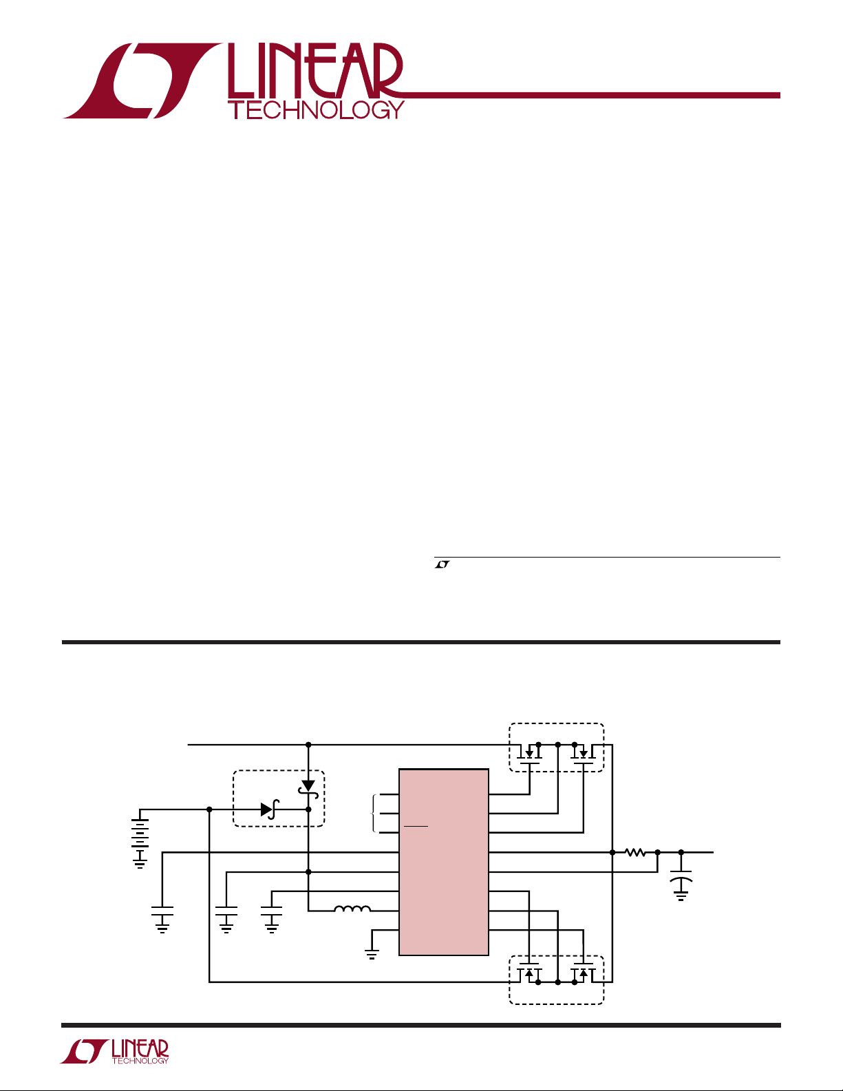
TYPICAL APPLICATIO
DCIN
3.3V
V
BAT1
4× NiMH
C
TIMER
2000pF
1µF
* COILCRAFT 1812LS-105XKBC
BAT54C
U
1µF
3.3V to 4-Cell NiMH Backup Switch
LOGIC
DRIVEN
1mH*
1
2
3
4
5
6
7
8
IN1
IN2
DIODE
TIMER
+
V
V
GG
SW
GND
LTC1473L
GA1
SAB1
GB1
SENSE
SENSE
GA2
SAB2
GB2
16
15
14
13
+
12
–
11
10
9
Si9926DY
Si9926DY
R
SENSE
0.04Ω
1473 TA01
3.3V OR
V
+
BAT1
C
OUT
1
LTC1473L
WW
W
ABSOLUTE AXI U RATI GS
(Note 1)
SENSE+, SENSE–, V+..................................–0.3 to 10V
GA1, GB1, GA2, GB2 ...................................–0.3 to 20V
SAB1, SAB2.................................................–0.3 to 10V
SW, VGG......................................................–0.3 to 20V
IN1, IN2, DIODE...........................................–0.3V to 7V
Junction Temperature (Note 2).............................125°C
Operating Temperature Range.....................0°C to 70°C
Storage Temperature Range................. –65°C to 150°C
Lead Temperature (Soldering, 10 sec)..................300°C
U
UUW
PACKAGE/ORDER I FOR A TIO
TOP VIEW
IN1
1
IN2
2
DIODE
3
TIMER
4
+
V
5
V
6
GG
SW
7
GND
8
GN PACKAGE
16-LEAD NARROW PLASTIC SSOP
T
= 125°C, θJA = 150°C/W
JMAX
16
15
14
13
12
11
10
9
GA1
SAB1
GB1
SENSE
SENSE
GA2
SAB2
GB2
+
–
ORDER PART
NUMBER
LTC1473LCGN
GN PART MARKING
1473L
Consult factory for Military and Industrial grade parts.
ELECTRICAL CHARACTERISTICS
The ● denotes the specifications which apply over the full operating
temperature range, otherwise specifications are at TA = 25°C. Test circuit, V+ = 5V, unless otherwise specified.
SYMBOL PARAMETER CONDITIONS MIN TYP MAX UNITS
+
V
I
S
V
GS
+
V
UVLO
+
V
UVLOHYS
V
HIDIGIN
V
LODIGIN
I
IN
V
GS(ON)
V
GS(OFF)
I
BSENSE
I
BSENSE
V
SENSE
I
PDSAB
I
TIMER
V
TIMER
t
ON
t
OFF
t
D1
t
D2
f
OVGG
Supply Operating Range 2.8 9 V
Supply Current V
IN1
= V
DIODE
= 5V, V
IN2
= 0V, V
SENSE
+
= V
–
= 5V ● 100 200 µA
SENSE
VGS Gate Supply Voltage VGS = VGG – V+, 2.8V ≤ V+ ≤ 10V (Note 3) ● 7.5 8.5 9.5 V
V+ Undervoltage Lockout Threshold V+ Ramping Down ● 2.3 2.5 2.8 V
V+ Undervoltage Lockout Hysteresis 70 mV
Digital Input Logic High (Note 4) ● 2 0.9 V
Digital Input Logic Low (Note 4) ● 0.6 0.4 V
Input Current V
Gate-to-Source ON Voltage I
Gate-to-Source OFF Voltage I
+
SENSE+ Input Bias Current V
–
SENSE– Input Bias Current V
Inrush Current Limit Sense Voltage V
SAB1, SAB2 Pull-Down Current V
Timer Source Current V
Timer Latch Threshold Voltage V
Gate Drive Rise Time C
Gate Drive Fall Time C
Gate Drive Turn-On Delay C
Gate Drive Turn-Off Delay C
= V
IN1
= I
GA1
= I
GA1
SENSE
V
SENSE
SENSE
V
SENSE
SENSE–
V
SENSE–
= V
IN1
= V
V
IN1
= 0.4V, V
IN1
V
SENSE
= 0.4V, V
IN1
= 1000pF, V
GS
= 1000pF, V
GS
= 1000pF, V
GS
= 1000pF, V
GS
= V
IN2
= I
GA2
= I
GA2
+
= V
SENSE
+
= V
SENSE
+
= V
SENSE–
+
= V
SENSE
= 10V (V
= 0V (V
= V
IN2
= 0.4V, V
IN2
+
– V
SENSE
= 5V ±1 µA
DIODE
= I
GB1
GB1
DIODE
IN2
IN2
= –1µA, V
GB2
= I
= 100µA, V
GB2
–
= 10V (Note 3) ● 24.510µA
–
= 0V (Note 5) ● –300 –175 –75 µA
= 10V (Note 3) ● 24.510µA
–
= 0V (Note 5) ● –300 –175 –75 µA
– V
SENSE+
SENSE+
– V
SENSE
SENSE
= 0.4V, V+ = 10V (Note 3) 5 20 35 µA
= 2V 30 140 300 µA
DIODE
= V
= V
SAB1
SAB1
SAB1
SAB1
= 2V, V
DIODE
–
= 300mV
= 2V ● 1.05 1.16 1.25 V
DIODE
= V
= 0V (Note 6) 33 µs
SAB2
= V
= 5V (Note 6) 2 µs
SAB2
= V
= 0V (Note 6) 22 µs
SAB2
= V
= 5V (Note 6) 1 µs
SAB2
= V
SAB1
SAB1
–
) (Note 3) 0.15 0.20 0.25 V
–
) 0.10 0.20 0.30 V
TIMER
= 5V ● 4.5 5.6 7.0 V
SAB2
= V
= 5V ● 0 0.4 V
SAB2
= 0V, ● 369µA
VGS Regulator Operating Frequency 30 kHz
2
ELECTRICAL CHARACTERISTICS
LTC1473L
Note 1: Absolute Maximum Ratings are those values beyond which the life
of a device may be impaired.
Note 2: T
dissipation P
is calculated from the ambient temperature TA and power
J
according to the following formula:
D
TJ = TA + (PD)(150°C/W)
Note 3: Some tests are performed under more stringent conditions to
ensure reliable operation over the entire supply voltage range.
Note 4: Digital inputs include: IN1, IN2 and DIODE.
Note 5: I
increases by the same amount as I
S
their common mode falls below 5V.
Note 6: Gate turn-on and turn-off times are measured with no inrush
current limiting, i.e., V
4.5V and fall times are measured from 4.5V to 1V. Delay times are
measured from the input transition to when the gate voltage has risen or
fallen to 3V. Results are not tested, but guaranteed by design.
UW
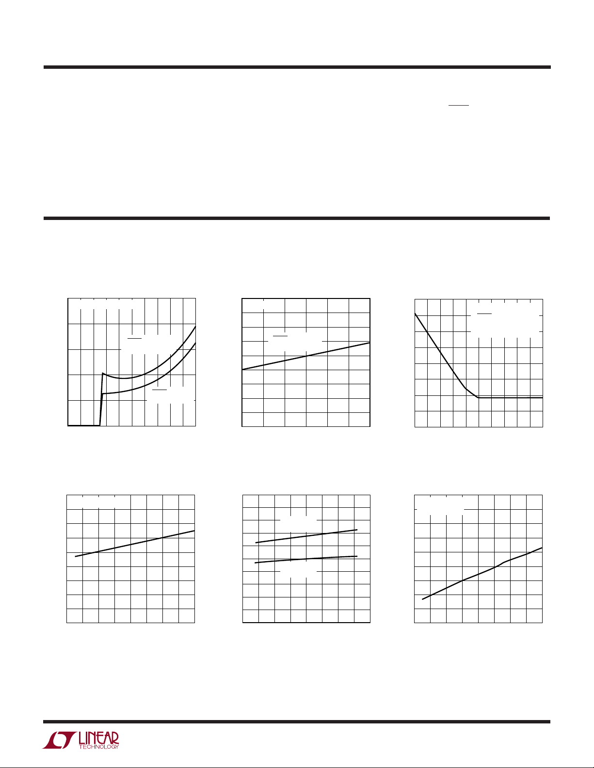
TYPICAL PERFOR A CE CHARACTERISTICS
DC Supply Current
vs Supply Voltage
250
200
150
100
SUPPLY CURRENT (µA)
50
0
0
V
SENSE
+
= V
2 45678913
+
–
= V
SENSE
V
= V
DIODE
IN1
V
IN2
V
DIODE
V
IN1
SUPPLY VOLTAGE (V)
= 5V
= 0V
= V
= 5V
IN2
= 0V
10
1473 G01
DC Supply Current
vs Temperature
140
V+ = 5V
130
120
110
100
90
80
SUPPLY CURRENT (µA)
70
60
50
–25 25 50 75 100
–50
V
= V
DIODE
TEMPERATURE (°C)
= 5V
IN1
V
= 0V
IN2
0
1473 G02
+
+ I
BSENSE
= 0V. Gate rise times are measured from 1V to
SENSE
DC Supply Current vs V
400
350
300
250
200
150
SUPPLY CURRENT (µA)
100
50
0
0
V
V+ = 5V
V
DIODE
V
IN2
V
SENSE
567 101234 89
COMMON MODE (V)
SENSE
BSENSE
= V
= 0V
+
– V
–
when
SENSE
= 5V
IN1
SENSE
–
= 0V
1473 G03
VGS Gate-to-Source ON Voltage
vs Temperature
6.0
V+ = V
= 10V
5.9
5.8
5.7
5.6
5.5
5.4
5.3
GATE-TO-SOURCE ON VOLTAGE (V)
GS
5.2
V
5.1
SAB
–60–40–20 204060800
TEMPERATURE (°C)
1473 G04
100
Undervoltage Lockout Threshold (V+)
vs Temperature
2.75
2.70
2.65
2.60
2.55
2.50
2.45
2.40
2.35
2.30
UNDERVOLTAGE LOCKOUT THRESHOLD (V)
2.25
–60
–40 0
START-UP
THRESHOLD
SHUTDOWN
THRESHOLD
–20
20
TEMPERATURE (°C)
40
VGS Gate Supply Voltage
vs Temperature
9.0
V+ = 5V
= VGG – V
V
8.9
GS
8.8
8.7
8.6
8.5
8.4
GATE SUPPLY VOLTAGE (V)
8.3
GS
V
8.2
80
60
100
1473 G05
8.1
–40–60
+
–20 20406080100
0
TEMPERATURE (°C)
1473 G06
3
LTC1473L
UW
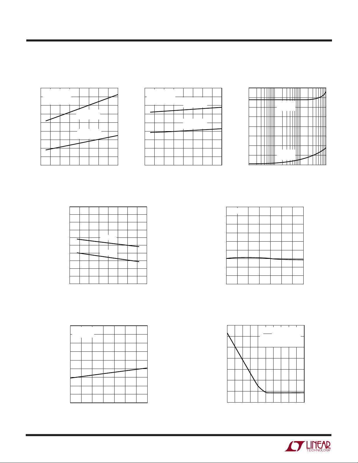
TYPICAL PERFOR A CE CHARACTERISTICS
Turn-Off Delay and Gate Fall Time
vs Temperature
2.2
+
= 5V
V
= 1000pF
C
2.0
LOAD
V
= 5V
SAB
1.8
1.6
1.4
1.2
1.0
0.8
0.6
TURN-OFF DELAY AND GATE FALL TIME (µs)
0.4
–20 20406080100
–40–60
GATE FALL
TIME
TURN-OFF
DELAY
0
TEMPERATURE (°C)
Logic Input Threshold Voltage
vs Temperature
2.0
1.8
1.6
1.4
1.2
1.0
0.8
0.6
0.4
INPUT THRESHOLD VOLTAGE (V)
0.2
0
–60
–40 0
–20
TEMPERATURE (°C)
1473 G07
V+ = 10V
V+ = 2.8V
20
Turn-On Delay and Gate Rise Time
vs Temperature
45
+
= 5V
V
40
35
30
25
20
15
10
5
TURN-ON DELAY AND GATE RISE TIME (µs)
0
= 1000pF
C
LOAD
V
= 0V
SAB
–40 –20 20 40 60 80 100
–60
TEMPERATURE (°C)
GATE RISE
TIME
TURN-ON
DELAY
0
1473 G08
Rise and Fall Time
vs Gate Capacitive Loading
40
35
30
25
20
15
10
RISE AND FALL TIME (µs)
5
0
10
RISE TIME
= 0V
V
SAB
FALL TIME
= 5V
V
SAB
100 1000 10000
GATE CAPACITIVE LOADING (pF)
1473 G08
Timer Latch Threshold Voltage
vs Temperature
1.28
V+ = 5V
1.26
1.24
1.22
1.20
1.18
1.16
1.14
1.12
TIMER LATCH THRESHOLD VOLTAGE (V)
80
60
40
100
1473 G10
1.10
–25 25 50 75 100 125
–50
0
TEMPERATURE (°C)
1473 G11
4
Timer Source Current
vs Temperature
8.5
V+ = 5V
TIMER = 0V
8.0
7.5
7.0
6.5
6.0
5.5
5.0
TIMER SOURCE CURRENT (µA)
4.5
4.0
–25 25 50 75 100 125
–50
0
TEMPERATURE (°C)
1473 G12
SENSE Pin Source Current
(I
300
250
200
150
100
50
SENSE PIN CURRENT (µA)
0
–50
0
) vs V
BSENSE
123456789
SENSE
V+ = 5V
V
V
V
V
SENSE
DIODE
= 0V
IN2
SENSE
(V)
= V
+
– V
IN1
SENSE
= 5V
–
= 0V
10
1473 G13
UUU
PI FU CTIO S
LTC1473L
IN1 (Pin 1): Logic Input of Gate Drivers GA1 and GB1. IN1
is disabled when IN2 is high or DIODE is low. During
2-diode mode, asserting IN1 disables the fault timer
function.
IN2 (Pin 2): Logic Input of Gate Drivers GA2 and GB2. IN2
is disabled when IN1 is high or DIODE is low. During
2-diode mode, asserting IN2 disables the fault timer
function.
DIODE (Pin 3): “2-Diode Mode” Logic Input. Diode overrides IN1 and IN2 by forcing the two back-to-back
external N-channel MOSFET switches to mimic two diodes.
TIMER (Pin 4): Fault Timer. A capacitor connected from
this pin to GND programs the time the MOSFET switches
are allowed to be in current limit. To disable this function,
Pin 4 can be grounded.
V+ (Pin 5): Power Supply. Bypass this pin with at least a
1µF capacitor.
VGG (Pin 6): Gate Driver Supply. This high voltage supply
is intended only for driving the internal micropower gate
drive circuitry.
circuitry
. Bypass this pin with at least 1µF.
Do not load this pin with any external
SW (Pin 7): Open Drain of an Internal N-Channel MOSFET
Switch. This pin drives the bottom of the VGG switching
regulator inductor which is connected between this pin and
the V+ pin.
GND (Pin 8): Ground.
GB2, GA2 (Pins 9, 11): Switch Gate Drivers. GA2 and GB2
drive the gates of the second back-to-back external
N-channel switches.
SAB2 (Pin 10): Source Return. The SAB2 pin is connected
to the sources of SW A2 and SW B2. A small pull-down
current source returns this node to 0V when the switches
are turned off.
SENSE– (Pin 12): Inrush Current Input. This pin should be
connected directly to the bottom (output side) of the low
valued resistor in series with the two input power selector
switch pairs, SW A1/B1 and SW A2/B2, for detecting and
controlling the inrush current into and out of the power
supply sources and the output capacitor.
SENSE+ (Pin 13): Inrush Current Input. This pin should be
connected directly to the top (switch side) of the low
valued resistor in series with the two input power selector
switch pairs, SW A1/B1 and SW A2/B2, for detecting and
controlling the inrush current into and out of the power
supply sources and the output capacitor. Current limit is
invoked when (V
Pin Function Table
PIN NAME DESCRIPTION MIN TYP MAX MIN MAX
1 IN1 Logic Input of Gate Drivers GA1 and GB1 0.4 1 2 –0.3 7
2 IN2 Logic Input of Gate Drivers GA2 and GB2 0.4 1 2 –0.3 7
3 DIODE “2-Diode Mode” Logic Input 0.4 1 2 –0.3 7
4 TIMER Fault Timer Programs Time in Current Limit 1.16 –0.3 5
5V+Power Supply 2.8 9 –0.3 10
6VGGGate Driver Supply 10.2 20 –0.3 20
7 SW Switch Node of Internal Boost Switching Regulator 0 20 –0.3 20
8 GND Ground 0 0 0
9 GB2 Switch Gate Driver for Switch B2 0 17 –0.3 20
10 SAB2 Source Return of Switch 2 0 10 –0.3 10
11 GA2 Switch Gate Driver for Switch A2 0 17 –0.3 20
12 SENSE
13 SENSE
14 GB1 Switch Gate Driver for Switch B1 0 17 –0.3 20
15 SAB1 Source Return of Switch 1 0 10 –0.3 10
16 GA1 Switch Gate Driver for Switch A1 0 17 –0.3 20
–
Inrush Current Input, Low Side 0 10 –0.3 10
+
Inrush Current Input, High Side 0 10 –0.3 10
NOMINAL (V) ABSOLUTE MAX (V)
SENSE
+
– V
SENSE
–
) exceeds ±0.2V.
5
 Loading...