

Linear Technology LTC1472 Datasheet
LTC1472
FEATURES
■
Both VCC and VPP Switching in a Single Package
■
Built-In Current Limit and Thermal Shutdown
■
16-Pin (Narrow) SOIC Package
■
Inrush Current Limited (Drives 150µF Loads)
■
Continuous 12V Power Not Required
■
Extremely Low R
■
Guaranteed 1A VCC Current and 120mA VPP Current
■
1µA Quiescent Current in Standby
■
No External Components Required
■
Compatible with Industry Standard Controllers
■
Break-Before-Make Switching
■
Controlled Rise and Fall Times
NMOS Switches
DS(ON)
U
APPLICATIONS
■
Notebook Computers
■
Palmtop Computers
■
Pen-Based Computers
■
Handi-Terminals
■
Bar-Code Readers
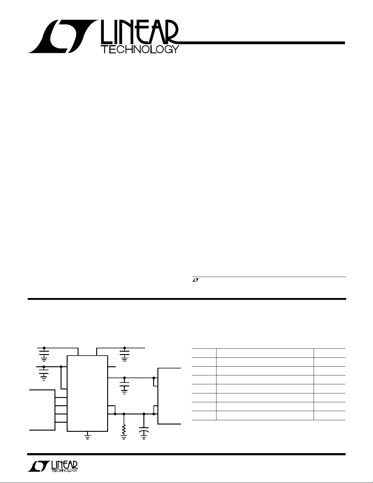
Protected PCMCIA V
CC
and
VPP Switching Matrix
U
DESCRIPTION
The LTC®1472 switching matrix routes power to both the
VCC and VPP power supply pins of the PCMCIA compatible
card socket. The V
between three operating states: OFF, 3.3V, and 5V. The
VPP output is switched between four operating states: 0V,
VCC, 12V, and Hi-Z. The output voltages are selected by
two sets of digital inputs which are compatible with
industry standard PC Card controllers (see Truth Tables).
The VCC output of the LTC1472 can supply up to 1A of
current and the VPP output up to 120mA. Both switches
have built-in SafeSlotTM current limiting and thermal shutdown to protect the card, socket and power supply against
accidental short-circuit conditions.
The LTC1472 is designed to conserve power by automatically dropping to 1µA standby current when the two
outputs are switched OFF. A shutdown pin is provided
which holds the external 12V regulator in standby mode
except when required for VPP power.
The LTC1472 is available in 16-pin SO.
, LTC and LT are registered trademarks of Linear Technology Corporation.
SafeSlot is a trademark of Linear Technology Corporation.
output of the LTC1472 is switched
CC
TYPICAL APPLICATION
Protected PCMCIA VCC and VPP Card Driver
3.3V
5V
CARD SLOT
CONTROLLER
PCMCIA
0.1µF
0.1µF
3V
IN
5V
IN
LTC1472
V
DD
VPP EN0
VPP EN1
V
EN0
CC
V
EN1
CC
GND
VPP
SHDN
VPP
V
CC(IN)
V
CC(OUT)
IN
TO 12V REGULATOR
OV, V
OUT
U
0.1µF
, 12V, Hi-Z
CC
0.1µF
OFF, 3.3V, 5V
+
10k
12V
1µF
VPP1
VPP2
PCMCIA
CARD SLOT
V
CC
V
CC
LTC1472-TA01
Linear Technology PCMCIA Product Family
DEVICE DESCRIPTION PACKAGE
LT®1312 Single PCMCIA VPP Driver/Regulator 8-Pin SO
LT1313 Dual PCMCIA VPP Driver/Regulator 16-Pin SO*
LTC1314 Single PCMCIA Switch Matrix 14-Pin SO
LTC1315 Dual PCMCIA Switch Matrix 24-Pin SSOP
LTC1470 Protected VCC 5V/3.3V Switch Matrix 8-Pin SO
LTC1471 Dual Protected VCC 5V/3.3V Switch Matrix 16-Pin SO*
LTC1472 Protected VCC and VPP Switch Matrix 16-Pin SO*
*Narrow Body
1
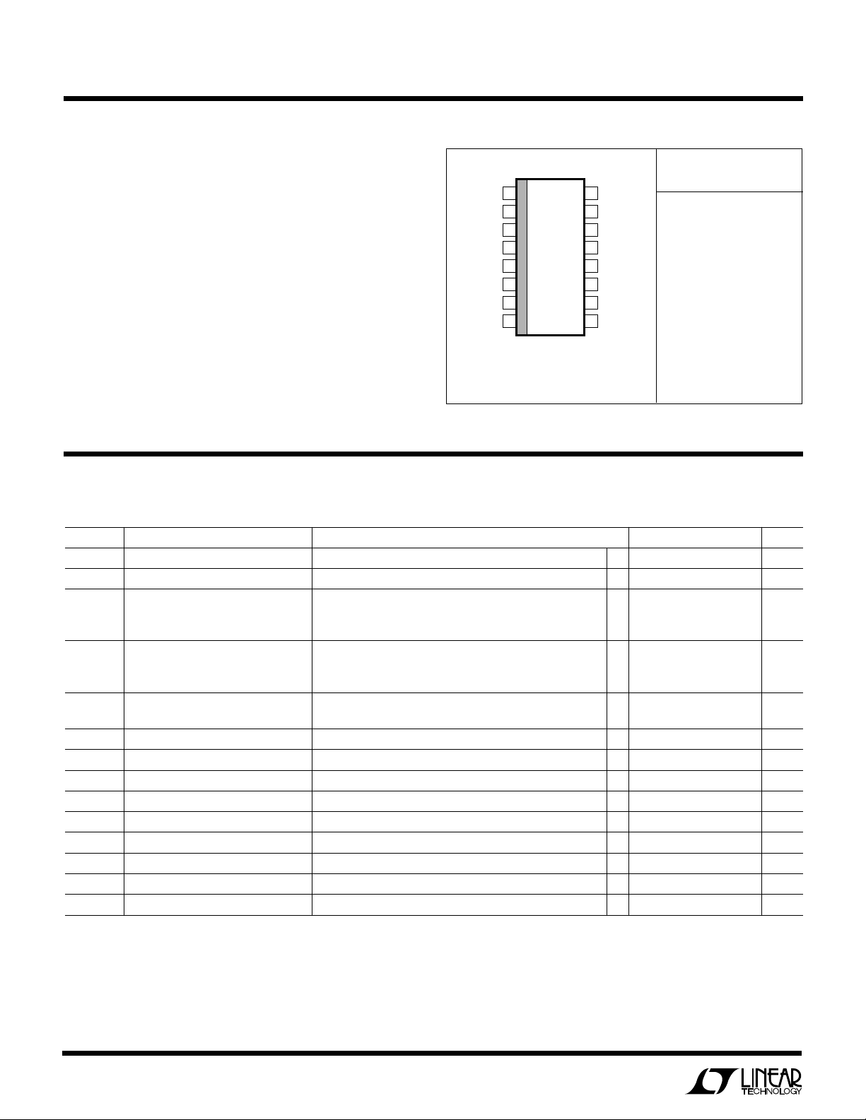
LTC1472
TOP VIEW
S PACKAGE
16-LEAD PLASTIC SO
T
JMAX
= 100°C, θJA = 100°C/W
1
2
3
4
5
6
7
8
16
15
14
13
12
11
10
9
V
CC(OUT)
5V
IN
V
CC
EN1
V
CC
EN0
VPP
IN
SHDN
VPP EN0
VPP EN1
V
CC(OUT)
3V
IN
3VIN
GND
V
CC(IN)
VPP
OUT
GND
V
DD
WW
W
ABSOLUTE MAXIMUM RATINGS
U
PACKAGE/ORDER INFORMATION
5VIN Supply Voltage ................................... – 0.3V to 7V
3VIN Supply Voltage ................................... –0.3V to 7V
VPPIN Supply Voltage ............................ –0.3V to 13.2V
V
V
VPP
V
Supply Voltage...................................–0.3 to 7V
CC(IN)
Supply Voltage ............................... –0.3V to 7V
DD(IN)
(OFF) ........................................ –0.3V to 13.2V
OUT
CC(OUT)
(OFF) ............................................ –0.3V to 7V
Enable Inputs.............................................. –0.3V to 7V
VPP
V
Short-Circuit Duration ........................ Indefinite
OUT
CC(OUT)
Short-Circuit Duration ....................... Indefinite
Operating Temperature Range ..................... 0°C to 70°C
Junction Temperature...........................................100°C
Storage Temperature Range ................. –65°C to 150°C
Lead Temperature (Soldering, 10 sec).................. 300°C
ELECTRICAL CHARACTERISTICS
5VIN = 5V, 3VIN = 3.3V, VPP EN0 = VPP EN1 = OV, TA = 25°C, (Note 1) unless otherwise noted.
(VCC Switch Section)
Consult factory for Industrial and Military grade parts.
U
ORDER PART
NUMBER
LTC1472CS
W
U
SYMBOL PARAMETER CONDITIONS MIN TYP MAX UNITS
5V
IN
3V
IN
I
5VIN
I
3VIN
R
ON
I
LKG
I
LIM5V
I
LIM3V
V
CCENH
V
CCENL
I
VCCEN
t
VCC1
t
VCC2
t
VCC3
2
5VIN Supply Voltage Range (Note 2) 4.75 5.25 V
3VIN Supply Voltage Range (Note 3) 0 3.60 V
5VIN Supply Current Program to Hi-Z ● 0.01 10 µA
Program to 5V, No Load
Program to 3.3V, No Load
3VIN Supply Current Program to Hi-Z. ● 0.01 10 µA
Program to 5V, No Load
Program to 3.3V, No Load
5V Switch On Resistance Program to 5V, I
3.3V Switch On Resistance Program to 3.3V, I
Output Leakage Current OFF V
V
5V Current Limit Program to 5V, V
CC(OUT)
V
3.3V Current Limit Program to 3.3V, V
CC(OUT)
VCC Enable Input High Voltage ● 2V
V
Enable Input Low Voltage ● 0.8 V
CC
V
Enable Input Current 0V ≤ V
CC
Delay + Rise Time From 0V to 3.3V, R
Delay + Rise Time From 3.3V to 5V, R
Delay + Rise Time From 0V to 5V, R
EN0 = V
CC
CCEN
= 500mA 0.14 0.18 Ω
OUT
= 500mA 0.12 0.16 Ω
OUT
EN1 = 0V or 5V, 0V ≤ V
CC
= 0V (Note 4) 1 A
CC(OUT)
= 0V (Note 4) 1 A
CC(OUT)
≤ 5V ● ±1 µA
= 100Ω, C
LOAD
LOAD
LOAD
= 100Ω, C
= 100Ω, C
LOAD
LOAD
LOAD
≤ 5V ● ±10 µA
CC(OUT)
= 1µF (Note 5) 0.2 0.32 1 ms
= 1µF (Note 5) 0.2 0.52 1 ms
= 1µF (Note 5) 0.2 0.38 1 ms
● 140 200 µA
● 100 160 µA
● 0.01 10 µA
● 40 80 µA
LTC1472
ELECTRICAL CHARACTERISTICS
VDD = 5V, V
= 5V, VPPIN = 12V, V
CC(IN)
CCEN0
= V
CCEN1
(VPP Switch Section)
= 0V, TA= 25°C, (Note 1), unless otherwise noted.
SYMBOL PARAMETER CONDITIONS MIN TYP MAX UNITS
V
CC(IN)
VPP
V
DD
I
CCIN
I
PPIN
I
DD
I
VPPOUT
R
ON
VPP
VPP
I
VPPEN
V
SDH
V
SDL
I
LIMVCC
I
LIMVPP
t
VPP1
t
VPP2
t
VPP3
t
VPP4
t
VPP5
t
VPP6
t
VPP7
t
VPP8
IN
ENH
ENL
VCC Input Voltage Range ● 3 5.5 V
VPP Input Voltage Range (Note 6) ● 0 12.6 V
Logic Supply Voltage Range (Note 7) ● 4.5 5.5 V
V
Supply Current, No Load Program to VPPIN or V
CC(IN)
Program to 0V or Hi-Z
VPPIN Supply Current, No Load Program to VPPIN or V
Program to 0V or Hi-Z
VDD Supply Current, No Load Program to VPP
Program to V
Program to V
IN
, VPPIN = 0V ● 85 150 µA
CC(IN)
, VPPIN = 12V ● 40 80 µA
CC(IN)
Program to 0V or Hi-Z
Hi-Z Output Leakage Current Program to Hi-Z, 0V < VPP
On Resistance VPP
On Resistance VPP
On Resistance VPP
to VPP
OUT
OUT
OUT
IN
to V
CC(IN)
to GND VDD = 5V, I
VPPIN = 12V, I
V
CC(IN)
= 120mA 0.50 1 Ω
LOAD
= 5V, I
= 5mA 1.70 5 Ω
LOAD
= 1mA 100 250 Ω
SINK
VPPIN = 12V ● 35 60 µA
CC(IN)
CC(IN)
< 12V ● 0.01 10 µA
OUT
● 0.01 10 µA
● 40 80 µA
● 0.01 10 µA
● 70 120 µA
● 0.01 10 µA
VPP Enable Input High Voltage VDD = 5V ● 2V
VPP Enable Input Low Voltage VDD = 5V ● 0.8 V
VPP Enable Input Current 0V < VPP EN < VDD ● ±1 µA
SHDN Output High Voltage Program to 0V, V
SHDN Output Low Voltage Program to VPPIN, I
VPP
Current Limit, V
OUT
VPP
Current Limit, VPP
OUT
CC(IN)
IN
Delay and Rise Time From 0V to V
Program to V
CC(IN)
Program to VPPIN, VPP
CC(IN)
or Hi-Z, I
CC(IN)
= 400µA ● 0.4 V
SINK
, VPP
= 0V (Note 4) 60 mA
OUT
= 0V (Note 4) 100 mA
OUT
= 400µA ● 3.5 V
LOAD
,VPPIN = 0V (Note 8) 5 15 50 µs
Delay and Rise Time From 0V to VPPIN (Note 8) 25 85 250 µs
Delay and Rise Time From V
Delay and Fall Time From VPPIN to V
to VPPIN (Note 8) 30 100 300 µs
CC(IN)
(Note 9) 5 15 50 µs
CC(IN)
Delay and Fall Time From VPPIN to 0V (Note 10) 10 35 100 µs
Delay and Fall Time From V
Output Turn-On Delay From Hi-Z to V
to 0V, VPPIN = 0V (Note 10) 10 30 100 µs
CC(IN)
(Note 8) 5 15 50 µs
CC(IN)
Output Turn-On Delay From Hi-Z to VPPIN (Note 8) 25 85 250 µs
The ● denotes the specifications which apply over the full operating
temperature range.
Note 1: V
ENH
= 5V, V
= 0V. See VCC and VPP Switch Truth Tables for
ENL
programming enable inputs for desired output states.
Note 2: Power for the V
from the 5V
power supply which must be continuously powered. 12V
IN
and 3.3V power is not required to control the NMOS V
input logic and charge pump circuitry is derived
CC
switches. (See
CC
Applications Information.)
Note 3: The two 3V
together and the two V
together. The 3V
supply input pins (14 and 15) must be connected
IN
supply pins do not need to be continuously powered
IN
output pins (1 and 16) must be connected
CC(OUT)
and may drop to 0V when not required.
Note 4: The V
and VPP output are protected with foldback current limit
CC
which reduces the short-circuit (0V) currents below peak permissible
current levels at higher output voltages.
Note 5: To 90% of final value.
Note 6: 12V power is only required when VPP
is programmed to 12V.
OUT
The external 12V regulator can be shutdown at all other times. Built-in
charge pumps power the internal NMOS switches from the 5V V
supply
DD
when 12V is not present.
Note 7: Power for the VPP input logic and charge pump circuitry is derived
from the V
Note 8: To 90% of the final value, C
Note 9: To 10% of the final value, C
Note 10: To 50% of the initial value, C
power supply which must be continuously powered.
DD
= 0.1µF, R
OUT
= 0.1µF, R
OUT
OUT
= 0.1µF, R
OUT
OUT
= 2.9k.
= 2.9k.
= 2.9k.
OUT
3
LTC1472
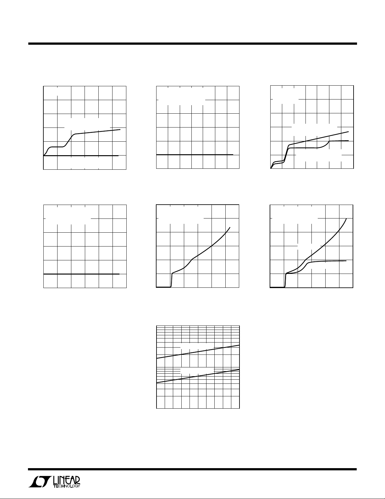
TIME (ms)
–0.2
INRUSH CURRENT (A)OUTPUT VOLTAGE (V)
0
1
1.4
LTC1472 TPC09
6
4
0
0.2
0.6
1.0
2
3
2
0
0.4
0.8
1.2
C
OUT
= 150µF
R
OUT
= 6.6Ω
C
OUT
= 150µF
R
OUT
= 6.6Ω
C
OUT
= 15µF
R
OUT
= 6.6Ω
TJ = 25°C
5VIN SUPPLY VOLTAGE (V)
0
0
5V
IN
SUPPLY CURRENT (µA)
50
100
150
200
300
1
234
LTC1472 TPC03
56
250
TA = 25°C V
CC(OUT)
PROGRAMMED
TO 3.3V, NO LOAD
W
U
TYPICAL PERFORMANCE CHARACTERISTICS
(VCC Section) VPP EN0 = VPP EN1 = 0V
5VIN Supply Current (OFF)
5
TA = 25°C V
PROGRAMMED TO OFF
4
3
2
1
SUPPLY CURRENT (µA)
IN
5V
0
–1
0
5
T
PROGRAMMED TO OFF
4
3
2
CC(OUT)
234
1
5VIN SUPPLY VOLTAGE (V)
= 25°C OUTPUT
A
5VIN Supply Current (5V ON) 5VIN Supply Current (3.3V ON)
56
LTC1472 TPC01
300
250
200
150
100
SUPPLY CURRENT (µA)
IN
5V
50
0
TA = 25°C V
PROGRAMMED
TO 5V, NO LOAD
0
1
5VIN SUPPLY VOLTAGE (V)
CC(OUT)
234
56
LTC1472 TPC02
5V Switch Resistance3VIN Supply Current (3.3V ON)3VIN Supply Current (OFF)
120
T
PROGRAMMED TO
100
3.3V, NO LOAD
80
60
= 25°C V
A
CC(OUT)
0.30
0.25
0.20
0.15
V
CC(OUT)
PROGRAMMED
TO 5V
SUPPLY CURRENT (µA)
3V
3.3V SWITCH RESISTANCE (Ω)
4
1
IN
0
–1
0
12
3VIN SUPPLY VOLTAGE (V)
3.3V Switch Resistance
0.30
V
CC(OUT)
PROGRAMMED
0.25
TO 3.3V
0.20
0.15
0.10
0.05
0
0
25 50 75 100
JUNCTION TEMPERATURE (°C)
3
LTC1472 TPC04
LT1472 TPC07
4
125
40
SUPPLY CURRENT (µA)
IN
3V
20
0
0
3
2
1
0
INRUSH CURRENT (A)OUTPUT VOLTAGE (V)
6
4
2
0
–0.2
12
3VIN SUPPLY VOLTAGE (V)
CURRENT
LIMITED
C
= 150µF
OUT
= 10Ω
R
OUT
0
0.2
0.6
0.4
TIME (ms)
C
OUT
R
OUT
0.8
1.0
3
LTC1472 TPC05
TJ = 25°C
= 15µF
= 10Ω
1.2
LTC1472 TPC08
4
1.4
0.10
5V SWITCH RESISTANCE (Ω)
0.05
0
0
25 50 75 100
JUNCTION TEMPERATURE (°C)
125
LT1472 TPC06
Inrush Current (3.3V Switch)Inrush Current (5V Switch)
VPPIN SUPPLY VOLTAGE
0
VPP
IN
SUPPLY CURRENT (µA)
80
100
120
610
LTC1472 TPC12
60
40
24
81214
20
0
TA = 25°C
VPP
IN
= 12V
NO LOAD
VPP
OUT
PROGRAMMED
TO V
CC(IN)
VPP
OUT
PROGRAMMED
TO VPP
IN
W
U
TYPICAL PERFORMANCE CHARACTERISTICS
V
100
80
Supply Current (No Load)
CC(IN)
TA = 25°C
VPPIN Supply Current (OFF) VPPIN Supply Current (No Load)
5
TA = 25°C
PROGRAMMED
VPP
OUT
4
TO 0V OR Hi-Z
LTC1472
(VPP Section) VCC EN0 = VCC EN1 = 0V
3
2
1
SUPPLY CURRENT (µA)
IN
VPP
0
–1
0
24
610
VPPIN SUPPLY VOLTAGE
81214
SUPPLY CURRENT (µA)
CC(IN)
V
–20
60
VPP
PROGRAMMED
OUT
OR V
TO VPP
IN
40
20
0
0
VPP
OUT
TO 0V OR Hi-Z
234
1
V
SUPPLY VOLTAGE (V)
CC(IN)
CC(IN)
PROGRAMMED
56
LTC1472 TPC10
VDD Supply Current (OFF) VDD Supply Current (No Load)
120
TA = 25°C
PROGRAMMED
VPP
100
SUPPLY CURRENT (µA)
DD
V
OUT
, NO LOAD
TO VPP
IN
80
60
40
20
0
0
234
1
VDD SUPPLY VOLTAGE (V)
SUPPLY CURRENT (µA)
DD
V
–1
5
TA = 25°C
VPP
4
TO 0V OR Hi-Z
3
2
1
0
0
PROGRAMMED
OUT
234
1
VDD SUPPLY VOLTAGE (V)
56
LTC1472 TPC13
LTC1472 TPC11
56
LTC1472 TPC14
VDD Supply Current (ON)
120
TA = 25°C
PROGRAMMED
VPP
100
SUPPLY CURRENT (µA)
DD
V
OUT
, NO LOAD
TO VPP
IN
80
60
40
20
0
0
VPPIN = 0V
234
1
VDD SUPPLY VOLTAGE (V)
VPPIN = 12V
56
LTC1472 TPC15
Switch Resistances
10
1
SWITCH RESISTANCE (Ω)
0.1
020406080
VCCIN TO VPP
VPPIN TO VPP
TEMPERATURE (°C)
OUT
OUT
100
LTC1472 TPC16
5
 Loading...