

Linear Technology LTC1456 Datasheet
FEATURES
■
SO-8 Package
■
12-Bit Resolution
■
Buffered True Rail-to-Rail Voltage Output
■
Asynchronous Clear Input
■
Built-In Reference
■
Schmitt Trigger On Clock Input Allows Direct
Optocoupler Interface
■
Power-On Reset Clears DAC to 0V
■
3-Wire Cascadable Serial Interface
■
Maximum DNL Error: 0.5LSB
■
Low Cost
U
APPLICATIONS
LTC1456
12-Bit Rail-to-Rail
Micropower DAC
with Clear Input
U
DESCRIPTION
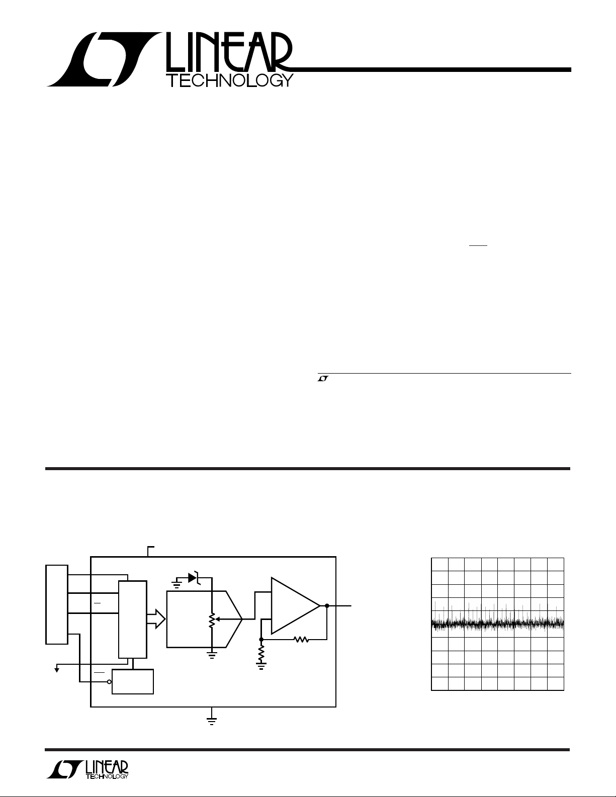
The LTC®1456 is a complete single supply, rail-to-rail
voltage output, 12-bit digital-to-analog converter (DAC) in
an SO-8 package. It includes a rail-to-rail output buffer
amplifier and an easy-to-use 3-wire cascadable serial
interface. The LTC1456 includes a CLR pin that asynchronously clears the DAC to zero scale.
The LTC1456 has an internal 2.048V reference and a fullscale output of 4.095V. It operates on a 4.5V to 5.5V
supply, dissipating 2.2mW.
The low power supply current and the space saving SO-8
package make the LTC1456 ideal for battery-powered
applications.
, LTC and LT are registered trademarks of Linear Technology Corporation.
■
Digital Calibration
■
Industrial Process Control
■
Automatic Test Equipment
■
Cellular Telephones
TYPICAL APPLICATION
Functional Block Diagram: 12-Bit Rail-to-Rail DAC with Clear Input
4.5V TO 5.5V
8
µP
TO
OTHER
DACS
D
2
IN
CLK1
CS/LD3
4
D
OUT
CLR6
V
12-BIT
SHIFT
REG
AND
DAC
LATCH
POWER-ON
RESET
2.048V
CC
12-BIT
DAC
U
GND
Differential Nonlinearity
vs Input Code
0.5
+
–
5
V
OUT
RAIL-TO-RAIL
7
VOLTAGE
OUTPUT
1456 TA01
0
DNL ERROR (LSB)
–0.5
512 1536 3072 3584
0
1024 2048 2560
CODE
4095
1456 TA02
1
LTC1456
WW
W
U
ABSOLUTE MAXIMUM RATINGS
VCC to GND .............................................. –0.5V to 7.5V
Logic Inputs to GND ................................ –0.5V to 7.5V
V
.............................................. –0.5V to VCC + 0.5V
OUT
Maximum Junction Temperature ......... –65°C to 125°C
Operating Temperature Range
LTC1456C ............................................ 0°C to 70°C
LTC1456I ........................................ –40°C to 85°C
Storage Temperature Range ................ –65°C to 150°C
Lead Temperature (Soldering, 10 sec)................. 300°C
PACKAGE
TOP VIEW
CLK
1
D
2
IN
CS/LD
3
D
4
OUT
N8 PACKAGE
8-LEAD PDIP
T
= 125°C, θJA = 100°C/W (N8)
JMAX
T
= 125°C, θJA = 150°C/W (S8)
JMAX
/
O
RDER I FOR ATIO
V
8
CC
V
7
OUT
CLR
6
GND
5
S8 PACKAGE
8-LEAD PLASTIC SO
S8 PART MARKING
WU
ORDER PART
NUMBER
LTC1456CN8
LTC1456IN8
LTC1456CS8
LTC1456IS8
1456
1456I
Consult factory for Military grade parts.
ELECTRICAL CHARACTERISTICS
VCC = 4.5V to 5.5V, V
SYMBOL PARAMETER CONDITIONS MIN TYP MAX UNITS
DAC
Resolution ● 12 Bits
DNL Differential Nonlinearity Guaranteed Monotonic (Note 1) ● ±0.5 LSB
INL Integral Nonlinearity TA = 25°C ±3.5 LSB
V
OS
VOSTC Offset Error Temperature ±15 µV/°C
V
FS
VFSTC Full-Scale Voltage ±24 ppm/°C
Power Supply
V
CC
I
CC
Op Amp DC Performance
AC Performance
Offset Error TA = 25°C ±12 mV
Coefficient
Full-Scale Voltage TA = 25°C 4.065 4.095 4.125 V
Temperature Coefficient
Positive Supply Voltage For Specified Performance ● 4.5 5.5 V
Supply Current (Note 4) ● 430 650 µA
Short-Circuit Current Low V
Short-Circuit Current High V
Output Impedance to GND Input Code = 0 ● 40 120 Ω
Voltage Output Slew Rate (Note 2) ● 0.4 1.0 V/µs
Voltage Output Settling Time (Notes 2, 3) to ±0.5LSB 14 µs
Digital Feedthrough 0.3 nV• s
unloaded, TA = T
OUT
to T
MIN
(Note 1)
Shorted to GND ● 120 mA
OUT
Shorted to V
OUT
, unless otherwise noted.
MAX
CC
● ±4 LSB
● ±18 mV
● 4.045 4.095 4.145 V
● 120 mA
U
2
LTC1456
ELECTRICAL CHARACTERISTICS
VCC = 4.5V to 5.5V, V
SYMBOL PARAMETER CONDITIONS MIN TYP MAX UNITS
Digital I/O
V
IH
V
IL
V
OH
V
OL
I
LEAK
C
IN
Switching
t
1
t
2
t
3
t
4
t
5
t
6
t
7
t
8
t
9
t
10
Digital Input High Voltage ● 2.4 V
Digital Input Low Voltage ● 0.8 V
Digital Output High Voltage I
Digital Output Low Voltage I
Digital Input Leakage VCC = 5V, VIN = GND to V
Digital Input Capacitance Guaranteed by Design. Not Subject to Test. ● 10 pF
DIN Valid to CLK Setup ● 40 ns
DIN Valid to CLK Hold ● 0ns
CLK High Time ● 40 ns
CLK Low Time ● 40 ns
CS/LD Pulse Width ● 50 ns
LSB CLK to CS/LD ● 40 ns
CS/LD Low to CLK ● 20 ns
D
Output Delay C
OUT
CLK Low to CS/LD Low ● 20 ns
CLR Pulse Width ● 65 ns
unloaded, TA = T
OUT
to T
MIN
= –1mA, D
OUT
= 1mA, D
OUT
= 15pF, VCC = 5V ● 150 ns
LOAD
, unless otherwise noted.
MAX
Only ● VCC – 1.0 V
OUT
Only ● 0.4 V
OUT
CC
● ±10 µA
The ● denotes specifications which apply over the full operating
temperature range.
Note 1: Nonlinearity is defined from the first code that is greater than or
equal to the maximum offset specification to code 4095 (full scale).
Note 2: Load is 5kΩ in parallel with 100pF.
Note 3: DAC switched between all 1s and the code corresponding to V
OS
for the part.
Note 4: Digital inputs at 0V or VCC.
3
 Loading...