

Linear Technology LTC1453, LTC1452, LTC1451 Datasheet
FEATURES
LTC1451
LTC1452/LTC1453
12-Bit Rail-to-Rail
Micropower DACs in SO-8
U
DESCRIPTIO
■
12-Bit Resolution
■
Buffered True Rail-to-Rail Voltage Output
■
3V Operation (LTC1453), ICC: 250µA Typ
■
5V Operation (LTC1451), ICC: 400µA Typ
■
3V to 5V Operation (LTC1452), ICC: 225µA Typ
■
Built-In Reference: 2.048V (LTC1451)
1.220V (LTC1453)
■
Multiplying Version (LTC1452)
■
Power-On Reset
■
SO-8 Package
■
3-Wire Cascadable Serial Interface
■
Maximum DNL Error: 0.5LSB
■
Schmitt Trigger on Clock Input Allows Direct
Optocoupler Interface
U
APPLICATIO S
■
Digital Calibration
■
Industrial Process Control
■
Automatic Test Equipment
■
Cellular Telephones
The LTC®1451/LTC1452/LTC1453 are complete single
supply, rail-to-rail voltage output 12-bit digital-to-analog
converters (DACs) in an SO-8 package. They include an
output buffer amplifier and an easy-to-use 3-wire
cascadable serial interface.
The LTC1451 has an onboard reference of 2.048V and a
full-scale output of 4.095V. It operates from a single 4.5V
to 5.5V supply.
The LTC1452 is a multiplying DAC with a full-scale output
of twice the reference input voltage. It operates from a
single supply of 2.7V to 5.5V.
The LTC1453 has an onboard 1.22V reference and a fullscale output of 2.5V. It operates from a single supply of
2.7V to 5.5V.
The low power supply current makes the LTC1451 family
ideal for battery-powered applications. The space saving
8-pin SO package and operation with no external components provide the smallest 12-bit DAC system available.
, LTC and LT are registered trademarks of Linear Technology Corporation.
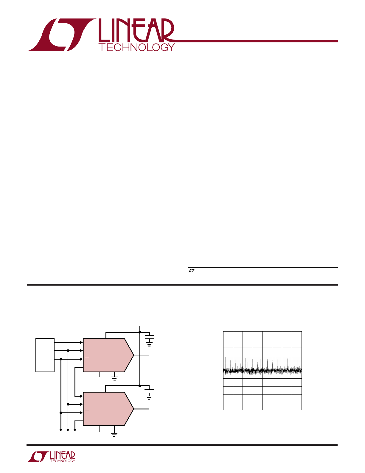
TYPICAL APPLICATIO
Daisy-Chained Control Outputs
V
µP
D
CLK
CS/LD
D
D
CLK
CS/LD
D
TO NEXT DAC
IN
OUT
IN
OUT
LTC1451
V
REF
LTC1451
V
REF
CC
GND
V
CC
GND
U
V
V
OUT
OUT
Differential Nonlinearity
5V
0.1µF
CONTROL
OUTPUT 1
0.1µF
CONTROL
OUTPUT 2
1451/2/3 TA01
0.5
0.0
DNL ERROR (LSB)
–0.5
0
vs Input Code
1024 2048 2560
512 1536 3072 3584
CODE
1451/2/3 TA02
4095
1
LTC1451
LTC1452/LTC1453
WWWU
ABSOLUTE AXI U RATI GS
(Note 1)
VCC to GND .............................................. –0.5V to 7.5V
TTL Input Voltage .................................... –0.5V to 7.5V
V
OUT
, D
.................................... –0.5V to VCC + 0.5V
OUT
REF ................................................ –0.5V to VCC + 0.5V
Maximum Junction Temperature ......... –65°C to 125°C
UU
W
PACKAGE/ORDER I FOR ATIO
TOP VIEW
CLK
1
D
2
IN
CS/LD
3
D
4
OUT
N8 PACKAGE
8-LEAD PDIP
T
= 125°C, θJA = 100°C/W (N8)
JMAX
T
= 125°C, θJA = 150°C/W (S8)
JMAX
Consult factory for Military grade parts.
8-LEAD PLASTIC SO
V
8
CC
V
7
OUT
REF
6
GND
5
S8 PACKAGE
LTC1451CN8
LTC1452CN8
LTC1453CN8
LTC1451IN8
LTC1452IN8
LTC1453IN8
Operating Temperature Range
Commercial ...........................................0°C to 70°C
Industrial ......................................... –40°C to 85°C
Storage Temperature Range ................ –65°C to 150°C
Lead Temperature (Soldering, 10 sec)................. 300°C
ORDER PART NUMBER
LTC1451CS8
LTC1452CS8
LTC1453CS8
LTC1451IS8
LTC1452IS8
LTC1453IS8
S8 PART MARKING
1451
1452
1453
1451I
1452I
1453I
ELECTRICAL CHARACTERISTICS
temperature range, otherwise specifications are at TA = 25°C. VCC = 4.5V to 5.5V (LTC1451), 2.7V to 5.5V (LTC1452/LTC1453),
internal or external reference (V
SYMBOL PARAMETER CONDITIONS MIN TYP MAX UNITS
DAC
Resolution ● 12 Bits
DNL Differential Nonlinearity Guaranteed Monotonic (Note 2) ● ±0.5 LSB
INL Integral Nonlinearity TA = 25°C ±3.5 LSB
V
OS
VOSTC Offset Error Temperature ±15 µV/°C
V
FS
VFSTC Full-Scale Voltage When Using Internal Reference, LTC1451 ±0.10 LSB/°C
Offset Error TA = 25°C ±12 mV
Coefficient
Full-Scale Voltage When Using Internal Reference, LTC1451, TA = 25°C 4.065 4.095 4.125 V
Temperature Coefficient When Using External 2.048V Reference, LTC1452 ±0.02 LSB/°C
≤ VCC/2), V
REF
(Note 2)
LTC1451
External 2.048V Reference, VCC = 5V, LTC1452 ● 4.075 4.095 4.115 V
When Using Internal Reference, LTC1453, TA = 25°C 2.470 2.500 2.530 V
LTC1453
When Using Internal Reference, LTC1453 ±0.10 LSB/°C
and REF unloaded, unless otherwise noted.
OUT
The ● denotes specifications which apply over the full operating
● ±4LSB
● ±18 mV
● 4.045 4.095 4.145 V
● 2.460 2.500 2.540 V
2
LTC1451
LTC1452/LTC1453
ELECTRICAL CHARACTERISTICS
The ● denotes specifications which apply over the full operating
temperature range, otherwise specifications are at TA = 25°C. VCC = 4.5V to 5.5V (LTC1451), 2.7V to 5.5V (LTC1452/LTC1453),
internal or external reference (V
SYMBOL PARAMETER CONDITIONS MIN TYP MAX UNITS
Reference (LTC1451/LTC1453)
Reference Output Voltage LTC1451 ● 2.008 2.048 2.088 V
Reference Output ±0.08 LSB/°C
Temperature Coefficient
Reference Line Regulation ● 0.7 ±2LSB/V
Reference Load Regulation 0 ≤ I
Reference Input Range V
Reference Input Resistance ● 81430 kΩ
Reference Input Capacitance 15 pF
Short-Circuit Current REF Shorted to GND ● 80 mA
Power Supply
V
CC
I
CC
Op Amp DC Performance
AC Performance
SINAD Signal-to-Noise + Distortion REF = 1kHz, 2V
Positive Supply Voltage For Specified Performance, LTC1451 ● 4.5 5.5 V
Supply Current 4.5V ≤ VCC ≤ 5.5V (Note 4), LTC1451 ● 300 400 620 µA
Short-Circuit Current Low V
Short-Circuit Current High V
Output Impedance to GND Input Code = 0 ● 40 120 Ω
Voltage Output Slew Rate (Note 3) ● 0.4 1.0 V/µs
Voltage Output Settling Time (Notes 3, 4) to ±0.5LSB 14 µs
Digital Feedthrough 0.3 nV• s
AC Feedthrough REF = 1kHz, 2V
≤ VCC/2), V
REF
LTC1453
LTC1453
REF
LTC1452
LTC1453
2.7V ≤ V
2.7V ≤ V
OUT
OUT
and REF unloaded, unless otherwise noted.
OUT
≤ 100µA, LTC1451 ● 0.2 ±1.5 LSB
OUT
≤ VCC – 1.5V ● VCC/2 V
≤ 5.5V (Note 4), LTC1452 ● 120 225 350 µA
CC
≤ 5.5V (Note 4), LTC1453 ● 150 250 500 µA
CC
Shorted to GND ● 100 mA
Shorted to V
CC
, LTC1452 –95 dB
P-P
, (Code: All 1s) LTC1452 85 dB
P-P
● 1.195 1.220 1.245 V
● 0.6 ±3 LSB
● 2.7 5.5 V
● 2.7 5.5 V
● 120 mA
3
LTC1451
LTC1452/LTC1453
ELECTRICAL CHARACTERISTICS
The ● denotes specifications which apply over the full operating
temperature range, otherwise specifications are at TA = 25°C. VCC = 5V (LTC1451LTC1452), VCC = 3V (LTC1453).
LTC1451/LTC1452 LTC1453
SYMBOL PARAMETER CONDITIONS MIN TYP MAX MIN TYP MAX UNITS
Digital I/O
V
IH
V
IL
V
OH
V
OL
I
LEAK
C
IN
Switching
t
1
t
2
t
3
t
4
t
5
t
6
t
7
t
8
t
9
Digital Input High Voltage ● 2.4 2.0 V
Digital Input Low Voltage ● 0.8 0.6 V
Digital Output High Voltage I
Digital Output Low Voltage I
Digital Input Leakage VIN = GND to V
= –1mA ● VCC – 1.0 VCC – 0.7 V
OUT
= 1mA ● 0.4 0.4 V
OUT
CC
● ±10 ±10 µA
Digital Input Capacitance Guaranteed by Design ● 10 10 pF
Not Subject to Test
DIN Valid to CLK Setup ● 40 60 ns
DIN Valid to CLK Hold ● 00 ns
CLK High Time ● 40 60 ns
CLK Low Time ● 40 60 ns
CS/LD Pulse Width ● 50 80 ns
LSB CLK to CS/LD ● 40 60 ns
CS/LD Low to CLK ● 20 30 ns
D
Output Delay C
OUT
= 15pF ● 150 220 ns
LOAD
CLK Low to CS/LD Low ● 20 30 ns
Note 1: Absolute Maximum Ratings are those values beyond which the life
of the device may be impaired.
Note 2: Nonlinearity is defined from the first code that is greater than or
equal to the maximum offset specification to code 4095 (full scale).
Note 3: Load is 5kΩ in parallel with 100pF.
Note 4: DAC switched between all 1s and the code corresponding to V
for the part, i.e., LTC1451: code 18; LTC1453: code 30.
Note 5: Digital inputs at 0V or VCC.
UW
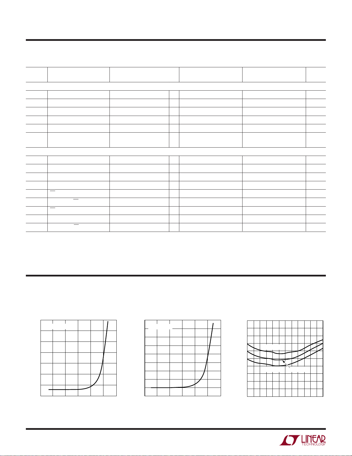
TYPICAL PERFOR A CE CHARACTERISTICS
LTC1451 Minimum Supply
Voltage vs Load Current
5.4
∆V
< 1LSB
OUT
5.2
5.0
4.8
4.6
4.4
MINIMUM SUPPLY VOLTAGE (V)
4.2
4.0
0.0001
0.010.001 0.1 100
LOAD CURRENT (mA)
110
1451/2/3 G01
LTC1453 Minimum Supply
Voltage vs Load Current
4.50
∆V
< 1LSB
0.0001
OUT
0.010.001 0.1 100
LOAD CURRENT (mA)
4.25
4.00
3.75
3.50
3.25
3.00
2.75
MINIMUM SUPPLY VOLTAGE (V)
2.50
2.25
110
1451/2/3 G02
LTC1451
Supply Current vs Temperature
450
440
430
420
410
400
390
380
SUPPLY CURRENT (µA)
370
360
350
–55
VCC = 5.5V
VCC = 4.5V VCC = 5V
–25
35 65
5
TEMPERATURE (°C)
95
1451/2/3 G03
OS
125
4
 Loading...