

查询DN266供应商
Multiple Power Supplies Track During Power Up
Design Note 272
Vladimir Ostrerov
advertisement
✩■▼❒❏❄◆❃▼❉❏■
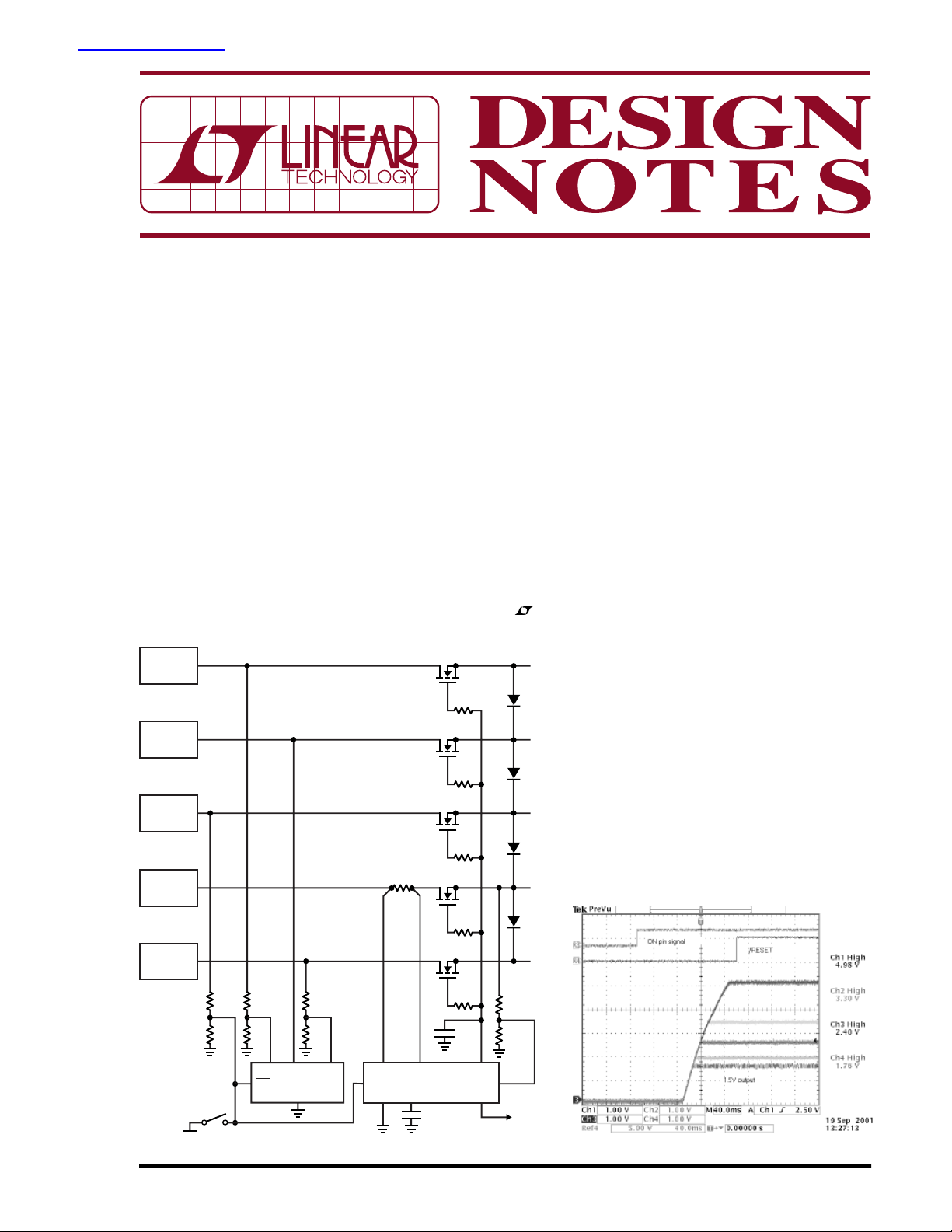
Many modern circuits require multiple power supplies
that must turn on in a certain order to avoid damaging
sensitive components. In many cases, forcing the supplies to ramp up together is the preferred solution.
Unfortunately, this can be difficult when the supplies are
generated from multiple sources, each with its own
power-up timing and transient response. However, there
is a simple solution for up to five supplies ramping up
simultaneously.
The circuit shown in Figure 1 solves this problem by
the circuit, the MOSFETs are turned off and each power
supply is allowed to power up at its own rate. Once each
power supply has settled, the common gates of the
MOSFETs are ramped up, forcing the outputs to ramp up
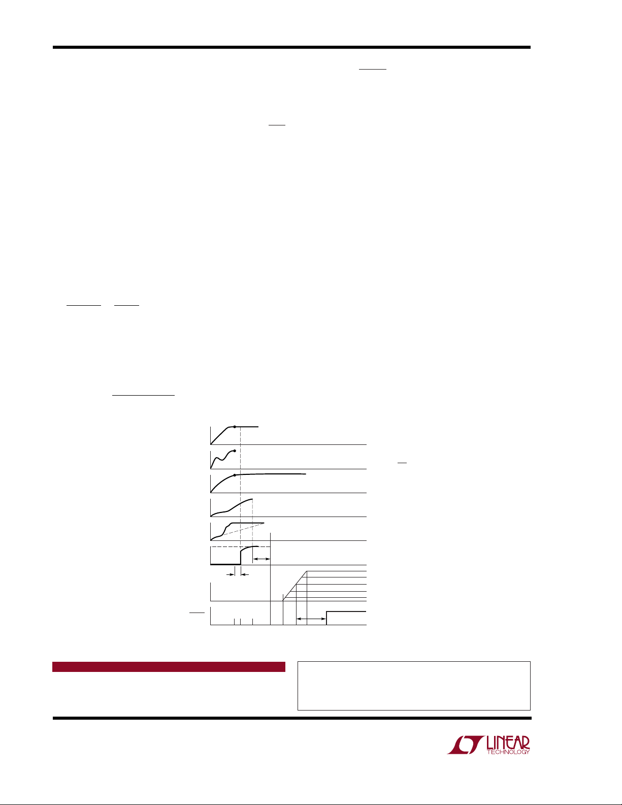
simultaneously as shown in Figure 2.
✦❉❖❅ ✳◆❐❐●❙ ✶❏●▼❁❇❅ ✴❒❁❃❋❅❒ ✣❉❒❃◆❉▼
The key components of the circuit in Figure 1 are the
LTC
single Hot Swap
monitors three supply outputs: 5V, 1.8V and 1.5V. The
outputs of the 3.3V and 2.5V supplies are monitored by
placing an N-channel MOSFET between the output of each
power supply and the load. When power is first applied to
Q1
R
S
0.005‰
Si4874
Si4874
Si4874
Si4874
21
4
Si4874
LTC1422
CT
0.33 F
R1
10‰
Q2
R2
10‰
Q3
R3
10‰
Q4
R4
10‰
Q5
R5
10‰
C1
0.1 F
1.5V 4A
DC/DC
CONVERTER
1.8V 4A
DC/DC
CONVERTER
2.5V 0.25A
DC/DC
CONVERTER
3.3V 10A
DC/DC
CONVERTER
5V 2A
DC/DC
CONVERTER
SW1
R6
931‰
R7
1.1k
R8
4.02k
R9
10k
RST
V
CCA
R10
1.82k
R11
2.8k
3
45
V
CC18
LTC1728-1.8
GND
3
V
CC3
87 6
CC
ON FB
Hot Swap is a trademark of Linear Technology Corporation.
R14
1.8k
R15
1.24k
GATESENSEV
RESETTIMERGND
DN268 F01
TO SYSTEM
¤
1728-1.8 triple supply monitor and the LTC1422
TM
controller. The LTC1728-1.8 directly
, LTC and LT are registered trademarks of Linear Technology Corporation.
1.5V
OUT
D1
MBR303
1.8V
OUT
D2
MBR303
D3
2.5V
OUT
D4
MBR303
3.3V
OUT
D5
MBR303
5V
OUT
10A
11/01/272
✦❉❇◆❒❅ ✑✎ ✕✍✳◆❐❐●❙ ✶❏●▼❁❇❅ ✴❒❁❃❋❅❒
✦❉❇◆❒❅ ✒✎ ✣❉❒❃◆❉▼ ✷❁❖❅❆❏❒❍▲
the LTC1422. Short-circuit protection for the 3.3V supply
is provided by the LTC1422 using sense resistor R
, but
S
all other voltages rely on their individual power supplys
current limit.
Once the 3.3V output is within tolerance as measured by
the FB pin, the RESET pin open-drain pull-down turns off
after a timing cycle. A complete timing diagram is shown
in Figure 3.
When all three supplies monitored by the LTC1728-1.8
are in compliance, the open-drain pull-down on the RST
pin turns off after a 200ms delay. The 2.5V resistor divider
monitor connected to the LTC1422 ON pin is then
enabled. When the 2.5V supply is within tolerance as
measured by the ON pin, and the 3.3V supply exceeds the
LTC1422 undervoltage lockout threshold, the LTC1422
turns on.
After one timing cycle (set by C2 at the TIMER pin), the
voltage at the GATE pin begins to ramp up, turning on
transistors Q1 to Q5. The slope of the voltage rise is set by
the total capacitance at the GATE pin (C
) and 0.1µA GATE
G
pull-up current:
Power down can be initiated by forcing the ON pin signal
low with the switch SW1, or by turning off any of the power
supplies. The GATE pin is pulled low immediately, disconnecting the loads from the power supplies, and the loads
start to discharge at the rate determined by the load
capacitance and load current. Diodes D1 to D5 are included
to insure worst-case differential levels between supplies
during power-down and catastrophic fault conditions.
For better performance, use low drop power MOSFETs
and adjust the preliminary power supply voltage to
account for the voltage drop across the transistor.
✣❏■❃●◆▲❉❏■
Although the circuit of Figure 1 controls five supplies, it
dV
GATE GATE
dt
Capacitance CG is equal to the sum of capacitor C1 and the
total MOSFET gate capacitance. Because each MOSFET is
connected as a source follower, the inrush current into
each load capacitance is limited according to:
I
INRUSH
I
=
C
G
CI
=
•
LOAD GATE
C
G
can be easily modified to accommodate fewer supplies.
Unused monitor inputs can be tied off to a higher supply
voltage and the unused MOSFETs removed. Different
supply voltages can be accommodated by selecting the
appropriate voltage option of the LTC1728-1.8 and changing resistor values. In sum, with only a handful of components, the circuit solves the tricky problem of controlling
the power up of multiple supplies in a complex system.
OUTPUT
VOLTAGES
✤❁▼❁ ✳❈❅❅▼ ✤❏◗■●❏❁❄
http://www.linear.com/go/dnLTC1422
1.5V
1.8V
5.5V
2.5V
3.3V
1.3V
T
TIMER
A1 A2
200ms
RESET
0ABCDD1F G
F′
✦❉❇◆❒❅ ✓✎ ✴❉❍❉■❇ ✤❉❁❇❒❁❍
0 TO A: ALL THREE POWER SUPPLY
OUTPUTS MONITORED
BY LTC1728-1.8 ARE WITHIN
ACCEPTABLE LIMITS
A TO B: 200ms DELAY IN BEFORE
RST IS GENERATED
C: TIME WHEN 2.5V OUTPUT DIVIDER
REACHES ON (LTC1422)
THRESHOLD LEVEL
C TO D: LTC1422 TIMER PERIOD
D TO D1: GATE VOLTAGE GROWS FROM
ZERO TO MOSFET THRESHOLD
F: TIME WHEN 2.5V OUTPUT IS
IN THE APPROPRIATIVE STATE
G:RESET GENERATED AFTER
TIMING CYCLE
5.5V
3.3V
2.5V
1.8V
1.5V
T
TIME
DN268 F03
For literature on our Hot Swap Controllers,
call ✑✍✘✐✐✍✔✍✬✩✮✥✡✲. For applications help,
call (408) 432-1900, Ext. 2453
Linear Technology Corporation
1630 McCarthy Blvd., Milpitas, CA 95035-7417
(408) 432-1900 ● FAX: (408) 434-0507 ● www.linear.com
dn272f LT/TP 1101 341.5K • PRINTED IN THE USA
LINEAR TECHNOLOGY CORPORATION 2001
 Loading...