

advertisement
Safe Hot Swapping Using the LTC1421 – Design Note 139
James Herr and Robert Reay
When a circuit board is inserted into a live backplane, the
large bypass capacitors on the board can draw huge inrush
currents from the backplane power bus as they charge. The
inrush current, on the order of 10A to 100A, can destroy the
board’s bypass capacitors, metal traces or connector pins.
The inrush current can also cause a glitch on the backplane
power bus, which could force all of the other boards in the
system to reset. In addition, the system data bus can be
disrupted when the board’s data pins make or break
contact.
The LTC
®
1421 can turn on two positive and one negative
board supply voltages at a programmable rate, allowing a
board to be safely inserted in, or removed from, a live
backplane. The device provides internal charge pumps for
V
EE
V
DD
Q1
MTB50N06E
10Ω
SETLO GATELO V
GND DISABLE
OUTLO
LTC1421
512
V
FAULT
POR
GND
DATA
BUS
R1
C1
1µF
0.005Ω
23
V
CCLO
2
CON2
24
AUXV
CC
4
FAULT
3
POR
1
CON1
CC
STAGGERED CONNECTOR
S1
PC BOARDBACKPLANE
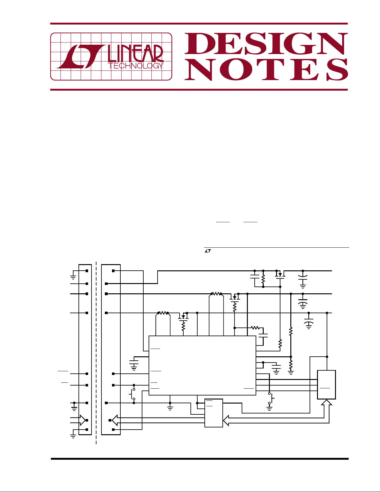
Figure 1. LTC1421 Typical Application
driving the gates of external N-channel pass transistors,
board connection sensing, flexible supply voltage monitoring, power on reset output, short-circuit protection and
soft or hard reset via software control.
Typical Application
Figure 1 shows a typical application using the LTC1421.
The LTC1421 works best with a staggered, 3-level connec-
tor. Ground makes connection first to discharge any static
build-up. V
, VDD and VEE make connection second and
CC
the data bus and all other pins last. The connection sense
pins CON1 and CON2 are located on opposite ends of the
connector to allow the board to be rocked back and forth
during insertion.
,LTC and LT are registered trademarks of Linear Technology Corporation.
0.025Ω
V
CCHI
1
BEA
13
BEB
12
GND
QS3384
QuickSwitch
R2
1/2 Si4936DY
SETHI GATEHI V
V
CC
®
Q3
1/2 Si4936DY
R4
20k
5%
+
Q2
0.47µF
C3
+
10Ω
10k
16
171819202122
OUTHI
RAMP
CPON
COMP
COMP
REF
FB
COMPOUT
PWRGD
RESET
QuickSwitch IS A REGISTERED TRADEMARK
OF QUALITY SEMICONDUCTOR CORPORATION.
C2
0.1µF
10
9
14
–
13
+
8
11
15
6
7
S2
DATA BUS
1µF
R5
16k
5%
R6
107k
1%
R7
13.7k
1%
+
C5
220µF
C3
220µF
C4
220µF
µP
I/O
I/O
RESET
DN139 F01
V
EE
–12V
1A
V
DD
12V
1A
V
CC
5V
5A
02/04/139fa
The power supplies on the board are controlled by placing
external N-channel pass transistors Q1, Q2 and Q3 in the
power path for VCC, VDD and VEE, where VCC and VDD can
range from 3V to 12V, and V
from –5V to – 12V. By
EE
ramping up the voltage on the pass transistors’ gates at a
controlled rate, the transient surge current [I = (C)(dv/dt)]
drawn from the main backplane supply will be limited to a
safe value. The ramp rate is set by the value of capacitor C2.
The board’s data bus is buffered by a QS3384 QuickSwitch
from Quality Semiconductor. Disabling the QuickSwitch
via the DISABLE pin during board insertion and removal
prevents corruption of the system data bus.
Resistors R1 and R2 form an electronic circuit breaker
function that protects against excessive supply current.
When the voltage across the sense resistor is greater than
50mV for more than 20µs, the circuit breaker trips, imme-
diately turning off Q1 and Q2 while the FAULT pin is pulled
low. The device will remain in the tripped state until the POR
pin is pulsed low or the power on V
The circuit breaker can be defeated by shorting V
SETLO and V
to SETHI.
CCHI
CCLO
and V
CCHI
is cycled.
to
CCLO
The RESET signal is used to reset the system microcontroller. When the voltage on the V
pin rises above
OUTLO
the reset threshold, PWRGD immediately goes high and
RESET goes high 200ms later. When the V
OUTLO
supply
voltage drops below the reset threshold, PWRGD immediately goes low, and RESET goes low 60µs later, allowing
the PWRGD signal to be used as an early warning that a
reset is about to occur. When the FB is left floating, the reset
threshold is 4.65V; when the FB pin is tied to V
OUTLO
, the
reset threshold is 2.90V.
is released, PWRGD immediately goes high, followed 200ms
later by RESET.
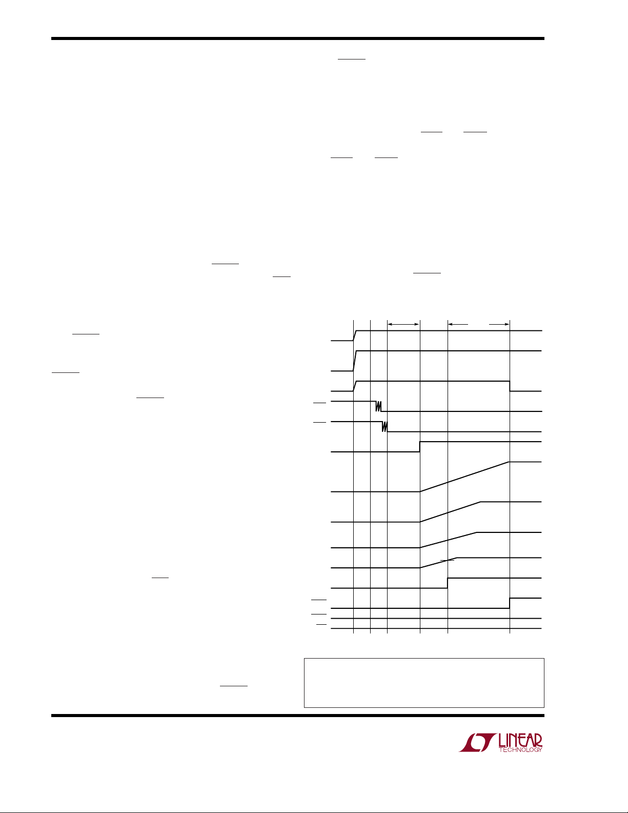
Board Insertion Timing
When the board is inserted, GND pin makes contact first,
followed by V
CCHI
and V
(Figure 2, time point 1).
CCLO
DISABLE is immediately pulled high, so the data bus switch
is disabled. At the same time CON1 and CON2 make contact
and are shorted to ground on the host side (time point 3).
When CON1 and CON2 are both forced to ground for more
than 20ms, the LTC1421 assumes that the board is fully
connected to the host and power-up can begin. When
V
CCLO
and V
exceed the 2.45V undervoltage lockout
CCHI
threshold, the 20µA current reference is connected from
RAMP to GND, the charge pumps are turned on and CPON
is forced high (time point 4). V
ramp up. When V
exceeds the reset threshold volt-
OUTLO
OUTHI
and V
OUTLO
begin to
age, PWRGD will immediately be forced high (time point
5). After a 200ms delay, RESET will be pulled high and
DISABLE will be pulled low, enabling the data bus (time
point 6).
V
CCLO
V
CCHI
DISABLE
CON1
CON2
CPON
123 4 5 6
20ms
200ms
The uncommitted comparator and internal voltage reference, along with resistors R6 and R7, are used to monitor
the 12V supply. When the supply drops below 10.8V, the
COMPOUT pin will go low. The comparator can be used to
monitor any voltage in the system.
Push-button switches S1 and S2 are used to generate a
hard and soft reset, respectively. A hard or soft reset may
also be initiated by a logic signal from the backplane.
Pushing S1 shorts the POR pin to ground, generating a
hard reset that cycles the board’s power. Pass transistors
Q1 to Q3 are turned off and V
pulled to ground. When V
OUTLO
OUTLO
and V
OUTHI
are actively
discharges to within 100mV
of ground, the LTC1421 is reset and a normal power-up
sequence is started.
Pushing S2 shorts the FB pin to ground, generating a soft
reset that doesn’t cycle the board’s power. PWRGD immediately goes low, followed 64µs later by RESET. When S2
Linear Technology Corporation
1630 McCarthy Blvd., Milpitas, CA 95035-7417
(408) 432-1900 ● FAX: (408) 434-0507 ● www.linear.com
GATEHI
V
OUTHI
GATELO
V
OUTLO
PWRGD
RESET
FAULT
POR
V
TH1
Figure 2. Board Insertion Timing
For applications help,
call (408) 432-1900, Ext. 2452
dn139fa web 0204 LT/GP 1096 180K • PRINTED IN THE USA
LINEAR TECHNOLOGY CORPORATION 1996
DN139 F02
 Loading...