

查询LTC1410CG供应商
FEATURES
■
Sample Rate: 2.5Msps
■
80dB S/(N + D) and 90dB THD at 100kHz f
■
Single 5V Operation
■
No Pipeline Delay
■
Programmable Input Ranges
■
Low Power Dissipation: 195mW (Typ)
■
True Differential Inputs Reject Common Mode Noise
■
Out-of-Range Indicator
■
Internal or External Reference
■
Sleep (1µA) and Nap (2mA) Shutdown Modes
■
36-Pin SSOP Package
IN
U
APPLICATIO S
■
Telecommunications
■
High Speed Data Acquisition
■
Digital Signal Processing
■
Multiplexed Data Acquisition Systems
■
Spectrum Analysis
■
Imaging Systems
, LTC and LT are registered trademarks of Linear Technology Corporation.
LTC1411
Single Supply
14-Bit 2.5Msps ADC
U
DESCRIPTIO
The LTC®1411 is a 2.5Msps sampling 14-bit A/D converter in a 36-pin SSOP package, which typically dissipates only 195mW from a single 5V supply. This device
comes complete with a high bandwidth sample-andhold, a precision reference, programmable input ranges
and an internally trimmed clock. The ADC can be powered
down with either the Nap or Sleep mode for low power
applications.
The LTC1411 converts either differential or single-ended
inputs and presents data in 2’s complement format.
Maximum DC specs include ±2LSB INL and 14-bit no
missing code over temperature. Outstanding dynamic
performance includes 80dB S/(N + D) and 90dB THD at
100kHz input frequency.
The LTC1411 has four programmable input ranges selected by two digital input pins, PGA0 and PGA1. This
provides input spans of ±1.8V, ±1.27V, ±0.9V and ±0.64V.
An out-of-the-range signal together with the D13 (MSB)
will indicate whether a signal is over or under the ADC’s
input range. A simple conversion start input and a data
ready signal ease connections to FIFOs, DSPs and microprocessors.
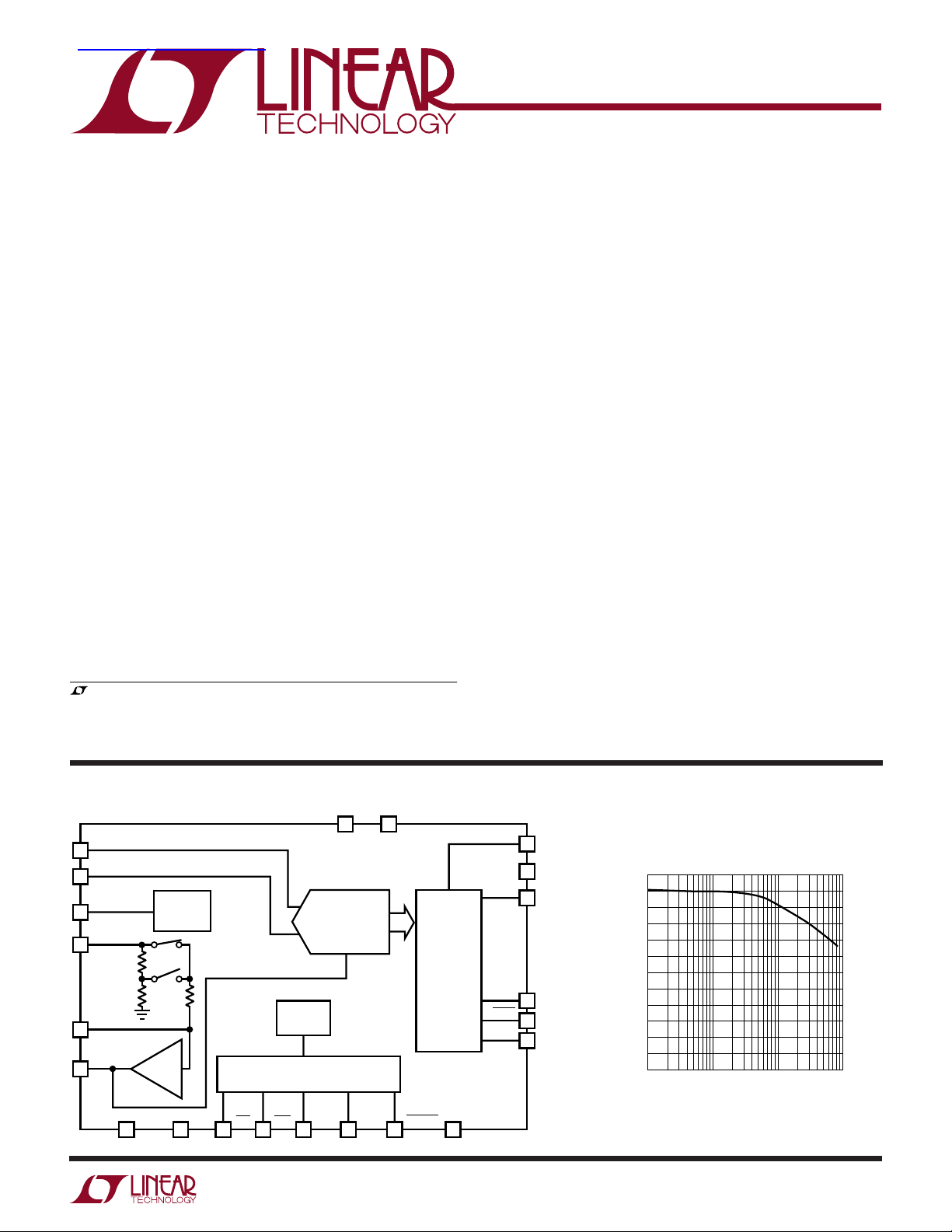
BLOCK DIAGRA
+
A
IN
1
–
A
IN
2
REFERENCE
5k
5k
X1.62/
X1.15
AGND
2.5V
BANDGAP
2k
AVM
REFOUT
3
REFIN
4
REFCOM1
5
REFCOM2
6
7, 8, 9
W
+
–
INTERNAL
CLOCK
CONTROL LOGIC
NAPSLP
PGA0
10
14-BIT
ADC
AVP
PGA1
30
14
323334353611
DVP
CONVST
OUTPUT
DRIVERS
31
DGND
OV
OGND
D13
BUSY
OTR
DD
29
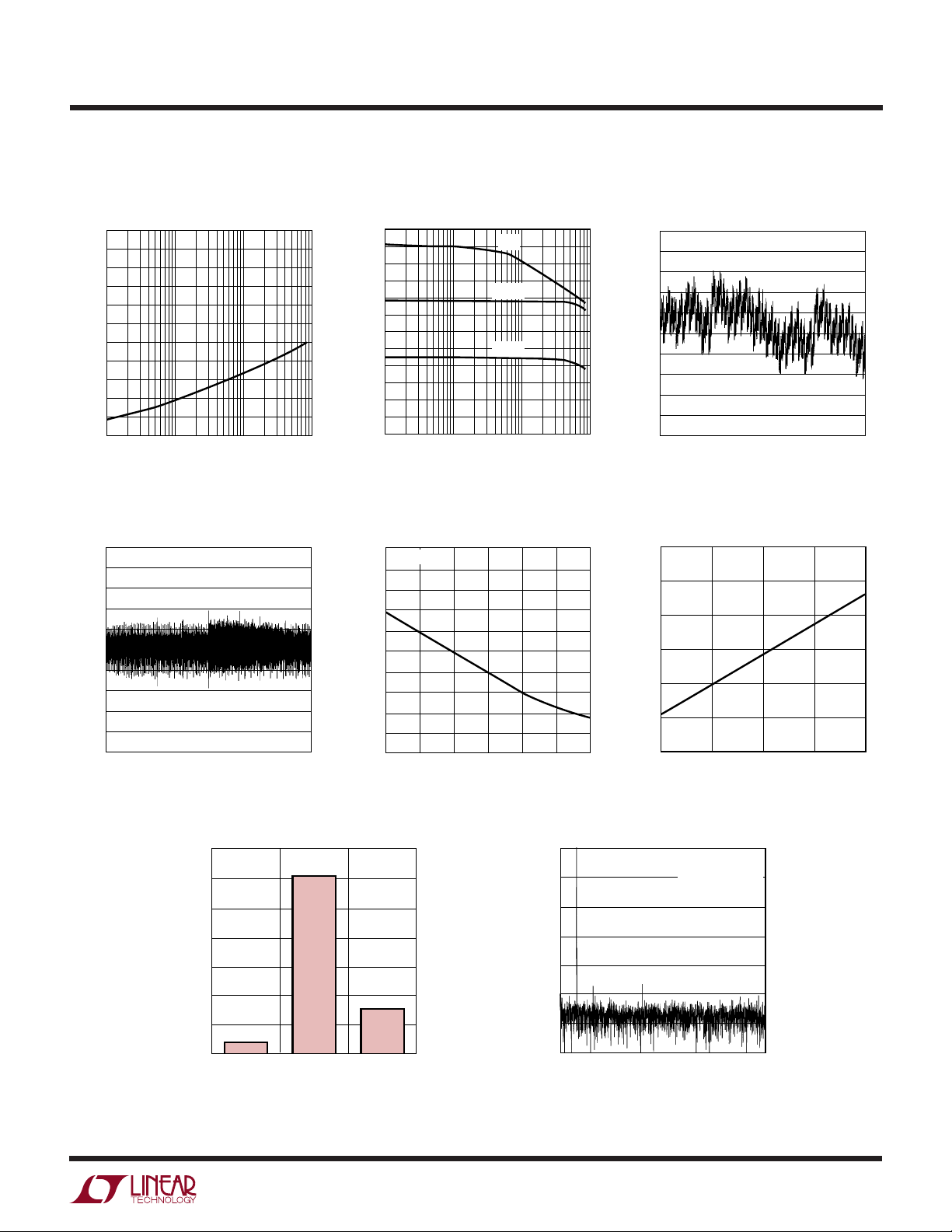
S/(N + D) and Effective Bits
vs Input Frequency
28
12
•
•
•
D0
25
27
26
1411 BD
86
80
74
68
62
56
50
44
S/(N + D) (dB)
38
32
26
20
14
10
100 1000 10000
INPUT FREQUENCY (kHz)
1411 TA02
14
13
12
11
EFFECTIVE BITS
10
1411f
1
LTC1411
WWWU
ABSOLUTE AXI U RATI GS
AVP = DVP = OV
Supply Voltage (VDD)................................................. 6V
Analog Input Voltage (Note 3) ... – 0.3V to (VDD + 0.3V)
Digital Input Voltage (Note 4) .................. – 0.3V to 10V
Digital Output Voltage............... – 0.3V to (VDD + 0.3V)
Power Dissipation.............................................. 500mW
Operating Temperature Range
LTC1411C ............................................... 0°C to 70°C
LTC1411I............................................ –40°C to 85°C
Storage Temperature Range ................. –65°C to 150°C
Lead Temperature (Soldering, 10 sec).................. 300°C
= VDD (Notes 1, 2)
DD
UU
W
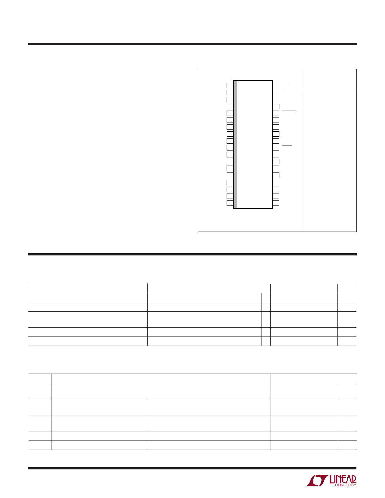
PACKAGE/ORDER I FOR ATIO
A
IN
A
IN
REFOUT
REFIN
REFCOM1
REFCOM2
AGND1
AGND2
AGND3
AVP
AVM
D13 (MSB)
D12
D11
D10
D9
D8
D7
TOP VIEW
+
1
–
2
3
4
5
6
7
8
9
10
11
12
13
14
15
16
17
18
G PACKAGE
36-LEAD PLASTIC SSOP
T
= 125°C, θJA = 95°C/W
JMAX
36
35
34
33
32
31
30
29
28
27
26
25
24
23
22
21
20
19
SLP
NAP
PGA0
PGA1
CONVST
DGND
DVP
OV
DD
OGND
BUSY
OTR
D0
D1
D2
D3
D4
D5
D6
ORDER PART
NUMBER
LTC1411CG
LTC1411IG
Consult LTC Marketing for parts specified with wider operating temperature ranges.
U
CO VERTER CHARACTERISTICS
temperature range, otherwise specifications are TA = 25°C. (Notes 5, 6)
PARAMETER CONDITIONS MIN TYP MAX UNITS
Resolution (No Missing Codes) ● 14 Bits
Integral Linearity Error (Note 7) ● ±2 LSB
Offset Error (Note 8) ±16 LSB
Full-Scale Error External Reference = 2.5V ±60 LSB
Full-Scale Tempco I
W
U
IC
DY
SYMBOL PARAMETER CONDITIONS MIN TYP MAX UNITS
S/(N + D) Signal-to-Noise Plus Distortion Ratio 100kHz Input Signal 80.0 dB
THD Total Harmonic Distortion 100kHz Input Signal, Up to 5th Harmonic –90 dB
A
Peak Harmonic or Spurious Noise 100kHz Input Signal 90 dB
Full Linear Bandwidth S/(N + D) ≥ 74dB 1.0 MHz
Transition Noise 0.66 LSB
ACCURACY
TA = 25°C (Note 5)
OUT(REF)
500kHz Input Signal 77.5 dB
500kHz Input Signal, Up to 5th Harmonic –82 dB
500kHz Input Signal 82 dB
The ● denotes specifications which apply over the full operating
● ±24 LSB
= 0 ±15 ppm/°C
RMS
2
1411f
LTC1411
UU
A ALOG I PUT
SYMBOL PARAMETER CONDITIONS MIN TYP MAX UNITS
V
IN
C
IN
t
ACQ
t
AP
t
jitter
CMRR Analog Input Common Mode Rejection Ratio 0V < (A
Analog Input Range (Note 9) (A
Common Mode Input Range A
Analog Input Capacitance Between Conversions (Sample Mode) 10 pF
Sample-and-Hold Acquisition Time 100 ns
Sample-and-Hold Aperture Delay Time 7 ns
Sample-and-Hold Aperture Delay Time Jitter 1 ps
Input Leakage Current (Pins 1, 2) 0.1 µA
TA = 25°C (Note 5)
+
–
) – (A
IN
+
(A
IN
+
(A
IN
+
(A
IN
+
or A
IN
During Conversions (Hold Mode) 4 pF
), PGA0 = PGA1 = 5V ±1.8 V
IN
–
) – (A
), PGA0 = 5V, PGA1 = 0V ±1.27 V
IN
–
) – (A
), PGA0 = 0V, PGA1 = 5V ±0.9 V
IN
–
) – (A
), PGA0 = PGA1 = 0V ±0.64 V
IN
–
IN
–
+
= A
IN
) < V
IN
DD
0V
62 dB
DD
RMS
UU U
I TER AL REFERE CE CHARACTERISTICS
PARAMETER CONDITIONS MIN TYP MAX UNITS
V
Output Voltage I
REF
V
Output Tempco I
REF
V
Line Regulation 4.75V ≤ VDD ≤ 5.25V 0.01 LSB/V
REF
V
Load Regulation 0 ≤ I
REF
REFCOM2 Output Voltage I
REFIN Input Current REFIN = External Reference 2.5V 250 µA
= 0 2.480 2.500 2.520 V
OUT
= 0 ±15 ppm/°C
OUT
≤ 1mA 2 LSB/mA
OUT
= 0, PGA0 = PGA1 = 5V 4.05 V
OUT
TA = 25°C (Note 5)
V
UU
DIGITAL I PUTS A D DIGITAL OUTPUTS
The ● denotes specifications which apply over the full operating temperature range, otherwise specifications are TA = 25°C. (Note 5)
SYMBOL PARAMETER CONDITIONS MIN TYP MAX UNITS
V
IH
V
IL
I
IN
C
IN
V
OH
V
OL
I
SOURCE
I
SINK
High Level Input Voltage V
Low Level Input Voltage VDD = 4.75V ● 0.8 V
Digital Input Current VIN = 0V to VDD, Except SLP, NAP (Note 11) ● ±10 µA
Digital Input Capacitance 2pF
High Level Output Voltage VDD = 4.75V, IO = –10µA 4.75 V
Low Level Output Voltage VDD = 4.75V, IO = 160µA 0.05 V
Output Source Current V
Output Sink Current V
= 5.25V ● 2.4 V
DD
VDD = 4.75V, IO = –200µA ● 4.0 V
VDD = 4.75V, IO = 1.6mA ● 0.10 0.4 V
= 0V –10 mA
OUT
OUT
= V
DD
10 mA
WU
POWER REQUIRE E TS
The ● denotes specifications which apply over the full operating temperature range, otherwise specifications are TA = 25°C. (Note 5)
SYMBOL PARAMETER CONDITIONS MIN TYP MAX UNITS
V
DD
I
DD
P
D
Supply Voltage (Note 9) 4.75 5.25 V
Supply Current ● 39 65 mA
Nap Mode NAP = 0V (Note 11) 2 mA
Sleep Mode SLP = 0V 1 µA
Power Dissipation ● 195 325 mW
Nap Mode NAP = 0V 10 mW
Sleep Mode SLP = 0V 5 µW
1411f
3
LTC1411
W
U
TI I G CHARACTERISTICS
range, otherwise specifications are TA = 25°C. (Notes 5) (See Figures 11a, 11b)
SYMBOL PARAMETER CONDITIONS MIN TYP MAX UNITS
f
SAMPLE(MAX)
t
CONV
t
ACQ
t
0
t
1
t
2
t
3
t
4
t
5
t
6
Note 1: Absolute Maximum Ratings are those values beyond which the life
of a device may be impaired.
Note 2: All voltage values are with respect to ground with DGND, OGND,
AVM and AGND wired together unless otherwise noted.
Note 3: When these pin voltages are taken below AGND or above V
they will be clamped by internal diodes. This product can handle input
currents greater than 100mA without latchup.
Note 4: When these pin voltages are taken below AGND, they will be
clamped by internal diodes. This product can handle input currents greater
than 100mA below AGND without latchup. These pins are not clamped to
V
.
DD
Note 5: V
tr = tf = 5ns unless otherwise specified.
Note 6: Linearity, offset and full-scale specifications apply for a singleended A
Maximum Sampling Frequency (Note 9) ● 2.5 MHz
Conversion Time ● 250 350 ns
Acquisition Time 100 ns
SLP↑ to CONVST↓ Wake-Up Time 10µF Bypass Capacitor at REFCOM2 Pin 210 ms
NAP↑ to CONVST↓ Wake-Up Time 250 ns
CONVST Low Time (Note 10) ● 20 ns
CONVST to BUSY Delay CL = 25pF 12 ns
Data Ready After BUSY↑ 7ns
CONVST High Time (Note 10) ● 20 ns
Aperture Delay of Sample-and-Hold 7 ns
= 5V, PGA1 = PGA0 = 5V, f
DD
+
input with A
IN
–
tied to an external 2.5V reference voltage.
IN
= 2.5MHz at 25°C and
SAMPLE
The ● denotes specifications which apply over the full operating temperature
Note 7: Integral nonlinearity is defined as the deviation of a code from a
straight line passing through the actual endpoints of the transfer curve.
The deviation is measured from the center of the quantization band.
Note 8: Bipolar offset is the offset voltage measured from –0.5LSB
DD
,
when the output code flickers between 0000 0000 0000 00 and
1111 1111 1111 11.
Note 9: Recommended operating conditions.
Note 10: The falling CONVST edge starts a conversion. If CONVST returns
high at a critical point during the conversion it can create small errors. For
best performance ensure that CONVST returns high within 20ns after
conversion start of after BUSY rises.
Note 11: SLP and NAP have an internal pull-down so the pins will draw
approximately 7µA when tied high and less than 1µA when tied low.
UW
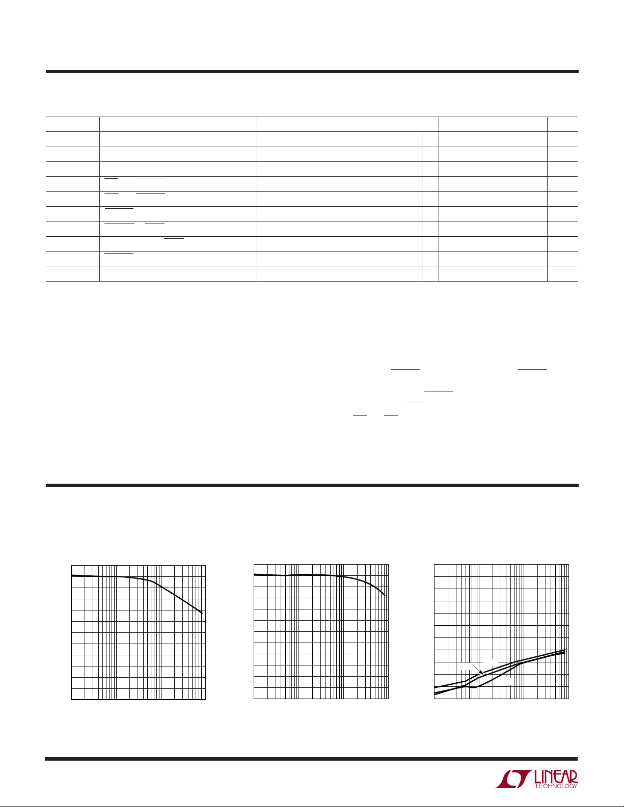
TYPICAL PERFOR A CE CHARACTERISTICS
Signal-to-Noise Ratio
S/(N + D) vs Input Frequency
86
80
74
68
62
56
50
44
S/(N + D) (dB)
38
32
26
20
14
10
100 1000 10000
INPUT FREQUENCY (kHz)
1411 G01
vs Input Frequency
86
80
74
68
62
56
50
SNR (dB)
44
38
32
26
20
14
10
100 1000 10000
INPUT FREQUENCY (kHz)
4
1411 G02
Distortion vs Input Frequency
0
–10
–20
–30
–40
–50
–60
–70
DISTORTION (dB)
–80
–90
–100
–110
10
THD
2ND
3RD
100 1000 10000
INPUT FREQUENCY (kHz)
1411 G03
1411f
UW
VDD (V)
4.5
31.5
SUPPLY CURRENT (mA)
34.0
36.5
39.0
41.5
44.0
46.5
T
A
= 25°C
4.75 5.0 5.25 5.5
1411 G12
TYPICAL PERFOR A CE CHARACTERISTICS
LTC1411
Spurious Free Dynamic Range
vs Input Frequency
0
–10
–20
–30
–40
–50
–60
–70
DISTORTION (dB)
–80
–90
–100
–110
10
100 1000 10000
INPUT FREQUENCY (kHz)
Differential Nonlinearity
vs Output Code
1.0
0.8
0.6
0.4
0.2
0
DNL (LSB)
–0.2
–0.4
–0.6
–0.8
–1.0
4096
0
8192
OUTPUT CODE
12288
1411 G04
16384
1411 G08
S/(N + D) vs Input Frequency
and Amplitude
86
80
74
68
62
56
50
44
SINAD (dB)
38
32
26
20
14
10
100 1000 10000
INPUT FREQUENCY (kHz)
0dB
–20dB
–40dB
Supply Current vs Temperature
45
VDD = 5V
44
43
42
41
40
39
38
SUPPLY CURRENT (mA)
37
36
35
–50
–25
25 50
0
TEMPERATURE (°C)
1411 G05
75 100
1411 G11
Integral Nonlinearity
vs Output Code
1.0
0.8
0.6
0.4
0.2
0
INL (LSB)
–0.2
–0.4
–0.6
–0.8
–1.0
4096
0
8192
OUTPUT CODE
12288
Supply Current vs Supply Voltage
16384
1411 G07
Histogram for 4096 Conversions
3500
3000
2500
2000
COUNTS
1500
1000
500
0
–1
01
CODE
1411 G13
4096 Points FFT Plot (100kHz)
0
–20
–40
–60
–80
AMPLITUDE (dB)
–100
–120
–140
250 500 750 1250
0
INPUT FREQUENCY (kHz)
SINAD = 78.8dB
SFDR = 95dB
f
= 2.5MHz
SAMPLE
= 100kHz
f
IN
1000
1411 G14
1411f
5

LTC1411
UW
TYPICAL PERFOR A CE CHARACTERISTICS
4096 Points FFT Plot (1MHz)
0
–20
–40
SINAD = 75dB
SFDR = 81dB
= 2.5MHz
f
SAMPLE
f
= 1MHz
IN
100
10
Acquisition Time
vs Source Resistance
–60
–80
AMPLITUDE (dB)
–100
–120
–140
U
250 500 750 1250
0
FREQUENCY (kHz)
UU
1000
1411 G15
PI FU CTIO S
+
A
(Pin 1):
IN
difference voltage between A
mable input ranges of ±1.8V, ±1.27V, ±0.9V and ±0.64V
depending on PGA selection. A
range between 0V and VDD.
–
A
(Pin 2): Negative Analog Input. This pin can be tied
IN
to the REFOUT pin of the ADC or tied to an external DC
voltage. This voltage is also the bipolar zero for the ADC.
–
A
has common mode range between 0V and VDD.
IN
REFOUT (Pin 3): 2.5V Reference Output. Bypass to AGND1
with a 22µF tantalum capacitor if REFOUT is tied to A
No capacitor is needed if the external reference is used to
drive A
REFIN (Pin 4): Reference Buffer Input. This pin can be
tied to REFOUT or to an external reference if more
precision is required.
REFCOM1 (Pin 5): Noise Reduction Pin. Put a 10µF
bypass capacitor at this pin to reduce the noise going into
the reference buffer.
REFCOM2 (Pin 6): 4.05V Reference Compensation Pin.
Bypass to AGND1 with a 10µF tantalum capacitor in
parallel with a 0.1µF ceramic.
Positive Analog Input. The ADC converts the
IN
+
and A
IN
IN
–
.
–
with program-
IN
+
has common mode
IN
–
.
1
ACQUISITION TIME (µs)
0.1
0.01
10
1
SOURCE RESISTANCE (Ω)
100
1000
10000
100000
1411 G16
AGND (Pins 7 to 9): Analog Ground. AGND1 is the ground
for the reference. AGND2 is the ground for the comparator
and AGND3 is the ground for the remaining analog
circuitry.
AVP (Pin 10): 5V Analog Power Supply. Bypass to AGND
with a 10µF tantalum capacitor.
AVM (Pin 11):
Analog and Digital Substrate Pin. Tie this
pin to AGND.
D13 to D0 (Pins 12 to 25): Digital Data Outputs. D13 is the
MSB (Most Significant Bit).
OTR (Pin 26): Out-of-the-Range Pin. This pin can be used
in conjunction with D13 to determine if a signal is less than
or greater than the analog input range. If D13 is low and
OTR is high, the analog input to the ADC exceeds the
maximum voltage of the input range.
BUSY (Pin 27): Busy Output. Converter status pin. It is
low during conversion.
OGND (Pin 28): Digital Ground for Output Drivers (Data
Bits, OTR and BUSY).
OVDD (Pin 29): 3V or 5V Digital Power Supply for Output
Drivers (Data Bits, OTR and BUSY). Bypass to OGND with
a 10µF tantalum capacitor.
6
1411f

LTC1411
U
UU
PI FU CTIO S
DVP (Pin 30): 5V Digital Power Supply Pin. Bypass to
OGND with a 10µF tantalum capacitor.
DGND (Pin 31): Digital Ground.
CONVST (Pin 32): Conversion Start Signal. This active
low signal starts a conversion on its falling edge.
PGA1, PGA0 (Pins 33, 34): Logic Inputs for Program-
mable Input Range. This ADC has four input ranges (or
four REFCOM2 voltages) controlled by these two pins.
For the logic inputs applied to PGA0 and PGA1, the
following summarizes the gain levels and the analog
input range with A
–
tied to 2.5V.
IN
WUUU
TYPICAL CO ECTIO DIAGRA
Table 1. Input Spans for LTC1411
INPUT REFCOM2
PGA0 PGA1 LEVEL SPAN VOLTAGE
5V 5V 0dB ±1.8V 4V
5V 0V –3dB ±1.28V 2.9V
0V 5V – 6dB ±0.9V 2V
0V 0V –9dB ±0.64V 1.45V
NAP (Pin 35): Nap Input. Driving this pin low will put the
ADC in the Nap mode and will reduce the supply current to
2mA and the internal reference will remain active.
SLP (Pin 36): Sleep Input. Driving this pin low will put the
ADC in the Sleep mode and the ADC draws less than 1µA
of supply current.
AVP DVP
PGA1
–
IN
5V
3010
14
323334353611
CONVST
OUTPUT
DRIVERS
31
DGND
OV
OGND
D13
D0
BUSY
OTR
DD
29
28
12
5V OR 3V
+
•
•
•
25
27
26
1411 TA01
+
+
A
IN
1
–
A
IN
2
REFERENCE
5k
5k
X1.62/
X1.15
AGND
2.5V
BANDGAP
2k
AVM
+
14-BIT
–
INTERNAL
CLOCK
CONTROL LOGIC
NAPSLP
PGA0
ADC
REFOUT
22µF*
10µF
10µF
3
REFIN
4
REFCOM1
5
REFCOM2
6
7, 8, 9
*A 22µF CAPACITOR IS NEEDED IF REFOUT IS USED TO DRIVE A
+
+
+
1411f
7

LTC1411
TEST CIRCUITS
Load Circuits for Access Timing Load Circuits for Output Float Delay
5V
1k
DNDN
1k
(A) Hi-Z TO VOH AND VOL TO V
C
L
(B) Hi-Z TO VOL AND VOH TO V
OH
C
L
OL
1411 TC01
WUUU
APPLICATIO S I FOR ATIO
CONVERSION DETAILS
The LTC1411 uses a successive approximation algorithm
and an internal sample-and-hold circuit to convert an
analog signal to a 14-bit parallel output. The ADC is
complete with a precision reference, internal clock and a
programmable input range. The device is easy to interface
with microprocessors and DSPs. (Please refer to the
Digital Interface section for the data format.)
Conversions are started by a falling edge on the CONVST
input. Once a conversion cycle has begun, it cannot be
restarted. Between conversions, the ADC acquires the
analog input in preparation for the next conversion.
acquire phase, a minimum time of 100ns will provide
enough time for the sample-and-hold capacitors to acquire the analog signal.
30
+
–
PGA0
10
14-BIT
ADC
+
A
IN
1
–
A
IN
2
INTERNAL
CLOCK
CONTROL LOGIC
NAPSLP
Figure 1. Simplified Block Diagram
AVP
PGA1
DVP
14
OUTPUT
DRIVERS
CONVST
3233343536 31
DGND
OV
OGND
D13
D0
BUSY
OTR
In the
DD
29
28
12
•
•
•
25
27
26
1411 F01
5V
1k
DNDN
1k
(A) VOH TO Hi-Z
C
L
(B) VOL TO Hi-Z
C
L
1411 TC02
During the conversion, the internal differential 14-bit
capacitive DAC output is sequenced by the SAR from the
most significant bit (MSB) to the least significant bit
(LSB). The input is successively compared with the binary
weighted charges supplied by the differential capacitive
DAC. Bit decisions are made by a high speed comparator.
At the end of a conversion, the DAC output balances the
analog input (A
IN
+
data word) which represents the difference of A
–
A
are loaded into the 14-bit output latches.
IN
– A
–
). The SAR contents (a 14-bit
IN
IN
+
and
DYNAMIC PERFORMANCE
The LTC1411 has excellent high speed sampling capability. FFT (Fast Fourier Transform) test techniques are used
to test the ADC’s frequency response, distortion and noise
at the rated throughput. By applying a low distortion sine
wave and analyzing the digital output using an FFT algorithm, the ADC’s spectral content can be examined for
frequencies outside the fundamental. Figure 2a shows a
typical LTC1411 FFT plot.
Signal-to-Noise
The signal-to-(noise + distortion) ratio [S/N + D)] is the
ratio between the RMS amplitude of the fundamental input
frequency to the RMS amplitude of all other frequency
components at the A/D output. The output is band limited
to frequencies from the above DC and below half the
sampling frequency. Figure 2a shows a typical spectral
content with a 2.5MHz sampling rate and a 100kHz input.
The dynamic performance holds well to higher input
frequencies (see Figure 2b).
1411f
8

WUUU
APPLICATIO S I FOR ATIO
0
–20
–40
–60
–80
AMPLITUDE (dB)
–100
–120
–140
0
250 500 750 1250
INPUT FREQUENCY (kHz)
SINAD = 78.8dB
SFDR = 95dB
f
= 2.5MHz
SAMPLE
= 100kHz
f
IN
1000
1411 G14
86
80
74
68
62
56
50
44
S/(N + D) (dB)
38
32
26
20
14
10
100 1000 10000
INPUT FREQUENCY (kHz)
1411 TA02
LTC1411
14
13
12
11
EFFECTIVE BITS
10
Figure 2a. LTC1411 Nonaveraged, 4096 Point FFT,
Input Frequency = 100kHz
0
SINAD = 75dB
SFDR = 81dB
–20
–40
–60
–80
AMPLITUDE (dB)
–100
–120
–140
= 2.5MHz
f
SAMPLE
f
= 1MHz
IN
250 500 750 1250
0
FREQUENCY (kHz)
1000
1411 G15
Figure 2b. LTC1411 4096 Point FFT,
Input Frequency = 1MHz
Effective Number of Bits
The effective number of bits (ENOBs) is a measurement of
the resolution of an ADC and is directly related to the
S/(N + D) by the equation:
ENOBS = [S/(N + D) – 1.76]/6.02
where S/(N + D) is expressed in dB. At the maximum
sampling rate of 2.5MHz the LTC1411 maintains good
ENOBs up to the Nyquist input frequency of 1.25MHz.
Refer to Figure␣ 3.
Total Harmonic Distortion
Total harmonic distortion (THD) is the ratio of the RMS
sum of all harmonics of the input signal to the fundamental
Figure 3. Effective Bits and Signal/(Noise + Distortion)
vs Input Frequency
0
–10
–20
–30
–40
–50
–60
–70
DISTORTION (dB)
–80
–90
–100
–110
10
THD
2ND
3RD
100 1000 10000
INPUT FREQUENCY (kHz)
1411 G03
Figure 4. Distortion vs Input Frequency
itself. The out-of-band harmonics alias into the frequency
band between DC and half the sampling frequency. THD is
expressed as:
2
2
22
4
V
1
N
THD
VVV V
+++…
2
=
20
log
3
where V1 is the RMS amplitude of the fundamental frequency and V2 through VN are the amplitudes of the
second through Nth harmonics. THD vs input frequency is
shown in Figure 4. The LTC1411 has good distortion
performance up to the Nyquist frequency and beyond.
1411f
9

LTC1411
WUUU
APPLICATIO S I FOR ATIO
Peak Harmonic or Spurious Noise
100
The peak harmonic or spurious noise is the largest spectral component excluding the input signal and DC. This
value is expressed in dB relative to the RMS value of a fullscale input signal.
Full-Power and Full-Linear Bandwidth
The full-power bandwidth is that input frequency at which
the amplitude of the reconstructed fundamental is reduced by 3db for a full-scale input signal.
The full-linear bandwidth is the input frequency at which
the S/(N + D) has dropped to 74dB (12 effective bits). The
LTC1411 has been designed to optimize input bandwidth,
allowing the ADC to undersample input signals with frequencies above the converter’s Nyquist frequency. The
noise floor stays very low at high frequencies; S/(N + D)
becomes dominated by distortion at frequencies far beyond Nyquist.
Driving the Analog Input
The differential analog inputs of the LTC1411 are easy to
drive. The inputs may be driven differentially or as a singleended input (i.e., the A
–
input is tied to a fixed DC voltage
IN
such as the REFOUT pin of the LTC1411 or an external
source). Figure 1 shows a simplified block diagram for the
analog inputs of the LTC1411. The A
IN
+
and A
IN
–
are
sampled at the same instant. Any unwanted signal that is
common mode to both inputs will be reduced by the
common mode rejection of the sample-and-hold circuit.
The inputs draw only one small current spike while charging the sample-and-hold capacitors at the end of conversion. During conversion, the analog inputs draw only a
small leakage current. If the source impedance of the
driving circuits is low, then the LTC1411 inputs can be
driven directly. More acquisition time should be allowed
for a higher impedance source. Figure 5 shows the acquisition time versus source resistance.
Choosing an Input Amplifier
Choosing an input amplifier is easy if a few requirements
are taken into consideration. First, to limit the magnitude
of the voltage spike seen by the amplifier from charging
10
1
ACQUISITION TIME (µs)
0.1
0.01
Figure 5. Acquisition Time vs Source Resistance
10
1
SOURCE RESISTANCE (Ω)
100
1000
10000
100000
1411 G16
the sampling capacitor, choose an amplifier that has a low
output impedance (<100Ω) at the closed-loop bandwidth
frequency. For example, if an amplifier is used in a gain of
1 and has a unity-gain bandwidth of 50MHz, then the
output impedance at 50MHz must be less than 100Ω. The
second requirement is that the closed-loop bandwidth
must be greater than 40MHz to ensure adequate smallsignal settling for full throughput rate. If slower op amps
are used, more settling time can be provided by increasing
the time between conversions.
The best choice for an op amp to drive the LTC1411 will
depend on the application. Generally applications fall into
two categories: AC applications where dynamic specifications are most critical and time domain applications where
DC accuracy and settling time are most critical. The
following list is a summary of the op amps that are suitable
for driving the LTC1411. More detailed information is
available in the Linear Technology Databooks and on the
LinearViewTM CD-ROM.
LT®1227: 140MHz Video Current Feedback Amplifier.
10mA supply current. ±5V to ±15V supplies. Low noise.
Good for AC applications.
LT1395: 400MHz Current Feedback Amplifier. Single 5V
or ±5V supplies. Good for AC applications.
LT1800: 80MHz, 25V/µs Low Power Rail-to-Rail Input and
Output Precision Op Amp. Specified at 3V, 5V and ±5V
supplies. Excellent DC performance.
LinearView is a trademark of Linear Technology Corporation.
10
1411f

WUUU
APPLICATIO S I FOR ATIO
LTC1411
LT6203: Dual 100MHz, Low Noise, Low Power Op Amp.
Specified at 3V, 5V and ±5V supplies. 1.9nV/√Hz noise
voltage.
Programmable Input Range
The LTC1411 has two logic input pins (PGA0 and PGA1)
that are used to select one of four analog input ranges.
These input ranges are set by changing the reference
voltage that is applied to the internal DAC of the ADC
(REFCOM2). For the “0dB” setting the internal DAC sees
the full reference voltage of 4V. The analog input range is
0.7V to 4.3V with A
span of ±1.8V with respect to the voltage applied to A
–
= 2.5V. This corresponds to an input
IN
IN
–
. For the “–3dB” setting the internal reference is reduced
to 0.707 • 4V = 2.9V. Likewise the input span is reduced
to ±1.28V. The following table lists the input span with
respect to A
Table 1. Input Spans for LTC1411
PGA0 PGA1 LEVEL SPAN VOLTAGE
5V 5V 0dB ±1.8V 4V
5V 0V – 3dB ±1.28V 2.9V
0V 5V – 6dB ±0.9V 2V
0V 0V – 9dB ±0.64V 1.45V
–
for the different PGA0 and PGA1 settings.
IN
INPUT REFCOM2
When changing from one input span to another, more time
is needed for the REFCOM2 pin to reach the correct level
because the bypass capacitor on the pin needs to be charged
or discharged. Figure 6 shows the recommended capacitors at the REFCOM1 and REFCOM2 pins (10µF each).
Internal Reference
The LTC1411 has an on-chip, temperature compensated,
curvature corrected, bandgap reference that is factory
trimmed to 2.500V. If this REFOUT pin is used to drive the
–
A
pin, a 22µF tantalum bypass capacitor is required and
IN
this REFOUT voltage sets the bipolar zero for the ADC.
The REFIN pin is connected to the reference buffer through
a 2k resistor and two PGA switches. The REFIN pin can be
connected to REFOUT directly or to an external reference.
Figure 6 shows the reference and buffer structure for the
LTC1411. The input to the reference buffer is either REFIN
or 1/2 of REFIN depending on the PGA selection. The
REFCOM1 pin bypassed with a 10µF tantalum capacitor
helps reduce the noise going into the buffer. The reference
buffer has a gain of 1.62 or 1.15 (depends on PGA
selection). It is compensated at the REFCOM2 pin with a
10µF tantalum capacitor. The input span of the ADC is set
by the output voltage of this REFCOM2 voltage. For a 2.5V
input at the REFIN pin, the REFCOM2 will have 4V output
for PGA1 = PGA0 = 5V and the ADC will have a span of 3.6V.
REFOUT
22µF**
REFIN*
REFCOM1
2.5V
BANDGAP
REFERENCE
5k
5k
2k
When –6dB or – 9dB is selected, the voltage at REFCOM1
(see Figure 2) must first settle before REFCOM2 reaches
the correct level. The typical delay is about 700ms.
When the REFCOM2 level is changed from 2.9V to 4V
(changing PGA setting from – 3dB to 0dB), the typical delay
is 0.6ms. However, if the voltage at REFCOM2 is changed
from 4V to 2.9V (changing PGA setting from 0dB to – 3dB)
only a 60µA sink current is present to discharge the 10µF
bypass capacitor. In this case, the delay will be 11ms.
10µF
REFCOM2
X1.62
10µF
*
THIS PIN CAN BE TIED TO REFOUT OR AN EXTERNAL SOURCE
**
A 22µF CAPACITOR IS NEEDED IF REFOUT IS USED TO DRIVE A
Figure 6. Reference Structure for the LTC1411
for PGA1 = PGA0 = 5V
1411 F06
–
IN
11
1411f

LTC1411
WUUU
APPLICATIO S I FOR ATIO
Figure 7 shows a typical reference, the LT1019A-2.5
connected to the LTC1411. This will provide an improved
drift (equal to the maximum 5ppm/°C of the LT1019A-2.5).
1
2
4
LTC1411
A
IN
A
IN
REFIN
AGND
7, 8, 9
5V
+
–
1411 F07
INPUT RANGE:
0.7V TO 4.3V
5V
2
V
IN
V
OUT
LT1019A-2.5
GND
4
6
3Ω
10µF
Figure 7. Supplying a 2.5V Reference Voltage
to the LTC1411 with the LT1019A-2.5
Digital Interface
The ADC has a very simple digital interface with only one
control input, CONVST. A logic low applied to the CONVST
input will initiate a conversion. The ADC presents digital
data in 2’s complement format with bipolar zero set by the
voltage applied to the A
IN
–
pin.
Internal Clock
The internal clock is factory trimmed to achieve a typical
conversion time of 260ns. With the typical acquisition
time of 100ns, a throughput sampling rate of 2.5Msps is
guaranteed.
Out-of-the-Range Signal (OTR)
The LTC1411 has a digital output, OTR, that indicates if an
analog input signal is out of range. The OTR remains
low when the analog input is within the specified range.
Once the analog signal goes to the most negative input
(1000 0000 0000 00) or 64LSB above the specified most
positive input, OTR will go high. By NORing D13 (MSB)
and its complement with OTR, overrange and underrange
can be detected as shown in Figure 8. Table 2 is the truth
table of the out-of-the-range circuit in Figure 8.
Power Shutdown (Sleep and Nap Modes)
The LTC1411 provides two shutdown features that will
save power when the ADC is inactive.
OTR
D13
D13
U1-A
U1-B
U1-A, U1-B = 74HC OR EQUIVALENT
“1” FOR OVERRANGE
“1” FOR UNDERRANGE
1411 F08
Figure 8. Overrange and Underrange Logic
Table 2. Out-of-the-Range Truth Table
OTR D13 (MSB) ANALOG INPUT
0 0 In Range
0 1 In Range
1 0 Overrange
1 1 Underrange
NAP
t
1
CONVST
1411 F09
Figure 9. NAP to CONVST Wake-Up Timing
By driving the SLP pin low for Sleep mode, the ADC shuts
down to less than 1µA. After release from the Sleep mode,
the ADC needs 210ms (10µF bypass capacitor on the
REFCOM2 pin) to wake up.
In Nap mode, all the power is off except the internal reference which is still active for the other external circuitry. In
this mode the ADC draws about 2mA instead of 39mA (for
minimum power, the logic inputs must be within 600mV
from the supply rails). The wake-up time from Nap mode
to active state is 250ns as shown in Figure 9.
Board Layout and Bypassing
Wire wrap boards are not recommended for high resolution or high speed A/D converters. To obtain the best
performance from the LTC1411, a printed circuit board
with a ground plane is required. Layout for the printed
circuit board should ensure that the digital and analog
signal lines are separated as much as possible. In particular, care should be taken not to run any digital track
alongside an analog signal track.
12
1411f

WUUU
APPLICATIO S I FOR ATIO
LTC1411
An analog ground plane separate from the logic system
ground should be established under and around the ADC.
AGND1, 2, 3 (Pins 7 to 9), AVM (Pin 11), DGND (Pin 31)
and OGND (Pin 28) and all other analog grounds should
be connected to a single analog ground point. The REFOUT,
REFCOM1, REFCOM2 and AVP should bypass to this
analog ground plane (see Figure 10). No other digital
grounds should be connected to this analog ground
plane. Low impedance analog and digital power supply
common returns are essential to low noise operation of
the ADC and the foil width for these tracks should be as
wide as possible.
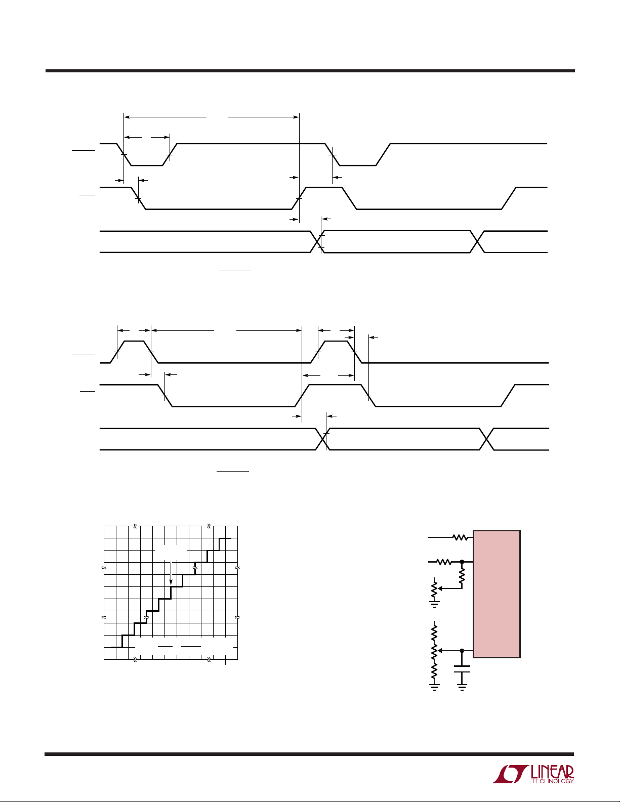
Timing and Control
Conversion start is controlled by the CONVST digital input.
The falling edge transition of the CONVST will start a
conversion. Once initiated, it cannot be restarted until the
conversion is complete. Converter status is indicated by
the BUSY output. BUSY is low during a conversion.
The digital output code is updated at the end of conversion
about 7ns after BUSY rises, i.e., output data is not valid on
the rising edge of BUSY. Valid data can be latched with the
falling edge of BUSY or with the rising edge of CONVST. In
either case, the data latched will be for the previous
conversion results. Figures 11a and 11b are the timing
diagrams for the LTC1411.
3V Input/Output Compatible
The LTC1411 operates on a 5V supply, which makes the
device easy to interface to 5V digital systems. This device
can also talk to 3V digital systems: the digital input pins
(CONVST, NAP and SLP) of the LTC1411 recognize 3V or
5V inputs. The LTC1411 has a dedicated output supply pin
(OVDD) that controls the output swings of the digital
output pins (D0 to D13, BUSY and OTR) and allows the
part to talk to either 3V or 5V digital systems. The output
is two’s complement binary.
Figure 12 is the input/output characteristics of the ADC
when A
–
= 2.5V. The code transitions occur midway
IN
between successive integer LSB values (i.e., 0.5LSB,
1.5LSB, 2.5LSB... FS – 1.5LSB). The output code is scaled
such that 1LSB = FS/16384 = 3.6V/16384 = 219.7µV.
Offset and Full-Scale Adjustment
In applications where absolute accuracy is important,
offset and full-scale errors can be adjusted to zero. Offset
error must be adjusted before full-scale error. Figure 13
shows the extra components required for full-scale error
adjustment. Zero offset is achieved by adjusting the
offset applied to the A
apply 2.49989V (i.e., –0.5LSB) at A
the A
–
input until the output code flickers between 0000
IN
–
input. For zero offset error,
IN
+
and adjust R2 at
IN
0000 0000 00 and 1111 1111 1111 11. For full-scale
adjustment, an input voltage of 4.29967V (FS – 1.5LSBs)
is applied to A
+
and R5 is adjusted until the output code
IN
flickers between 0111 1111 1111 10 and 0111 1111
1111 11.
ANALOG
INPUT
CIRCUITRY
1
+
A
IN
–
A
IN
2
REFOUT
3
+
–
REFIN
REFCOM1
4
REFCOM2
5
Figure 10. Power Supply Grounding Practice
6
AGND1
LTC1411
AGND2
7
8
AGND3
AVM
9
DVPAVP
11 10 30
OV
OGNDDGND
DD
31
29
28
1411 F10
DIGITAL
SYSTEM
1411f
13
LTC1411
WUUU
APPLICATIO S I FOR ATIO
t
CONV
(SAMPLE N)
t
2
CONVST
t
3
BUSY
t
ACQ
t
4
DATA
CONVST
BUSY
DATA
011...111
011...110
000...001
000...000
111...111
111...110
OUTPUT CODE
100...001
100...000
DATA (N – 1)
DB13 TO DB0
Figure 11a. CONVST Starts a Conversion with a Short Active Low Pulse
t
5
(SAMPLE N)
t
3
DATA (N – 1)
DB13 TO DB0
Figure 11b. CONVST Starts a Conversion with a Short Active High Pulse
BIPOLAR
ZERO
FS
16384
–1
LSB
2.5V
3.6V
16384
1
LSB
FS/2 – 1LSB–FS/2
1LSB = = = 219.7µV
INPUT VOLTAGE (V)
t
CONV
1411 F12
DATA N
DB13 TO DB0
t
5
t
3
t
ACQ
t
4
DATA N
DB13 TO DB0
R7
51Ω
R1
51Ω
R3
5V
51k
OFFSET
ADJUST
FULL-SCALE
ADJUST
R2
10k
5V
R4
100k
R5
750Ω
R6
100k
DATA (N + 1)
DB13 TO DB0
+
A
IN
–
A
IN
LTC1411
REFIN
1411 F11a
DATA (N + 1)
DB13 TO DB0
1411 F11b
1411 F13
Figure 12. LTC1411 Bipolar Transfer Characteristics
(2’s Complement)
14
Figure 13. Offset and Full-Scale Adjustment
1411f

PACKAGE DESCRIPTIO
5.20 – 5.38**
(.205 – .212)
U
G Package
36-Lead Plastic SSOP (5.3mm)
(Reference LTC DWG # 05-08-1640)
12345678 9 10 11 12 14 15 16 17 1813
12.67 – 12.93*
(.499 – .509)
LTC1411
2526 22 21 20 19232427282930313233343536
7.65 – 7.90
(.301 – .311)
1.73 – 1.99
(.068 – .078)
° – 8°
0
.13 – .22
(.005 – .009)
NOTE:
1. CONTROLLING DIMENSION: MILLIMETERS
2. DIMENSIONS ARE IN
3. DRAWING NOT TO SCALE
*
DIMENSIONS DO NOT INCLUDE MOLD FLASH. MOLD FLASH
SHALL NOT EXCEED .152mm (.006") PER SIDE
**
DIMENSIONS DO NOT INCLUDE INTERLEAD FLASH. INTERLEAD
FLASH SHALL NOT EXCEED .254mm (.010") PER SIDE
.55 – .95
(.022 – .037)
MILLIMETERS
(INCHES)
.65
(.0256)
BSC
.25 – .38
(.010 – .015)
.05 – .21
(.002 – .008)
G36 SSOP 0501
Information furnished by Linear Technology Corporation is believed to be accurate and reliable.
However, no responsibility is assumed for its use. Linear Technology Corporation makes no representation that the interconnection of its circuits as described herein will not infringe on existing patent rights.
1411f
15

LTC1411
TYPICAL APPLICATIO
+
A
IN
10µF
10µF
1
2
3
4
5
6
–
A
IN
REFOUT
REFIN
REFCOM1
REFCOM2
PROGRAMMABLE RANGE
DIFFERENTIAL INPUTS
(±0.64V TO ±1.8V)
+
+
U
2.5Msps 14-Bit ADC with Programmable Input Range
+
3010
AVP5VDVP
2.5V
BANDGAP
REFERENCE
5k
2k
5k
X1.62/
X1.15
+
14-BIT
–
INTERNAL
CLOCK
CONTROL LOGIC
ADC
14
OUTPUT
DRIVERS
OV
OGND
D13
BUSY
OTR
DD
29
28
12
•
•
•
D0
25
27
26
5V OR 3V
+
14-BIT
OUTPUT
DATA
7, 8, 9
AGND
AVM
323334353611
CONVST
NAPSLP
PGA0
5V
PGA1
DGND
31
2.5MHz CONVERT INPUT
INPUT RANGE
SELECTION
1411 TA03
RELATED PARTS
PART NUMBER RESOLUTION SPEED COMMENTS
16-Bit
LTC1608 16 500ksps ±2.5V Input Range, Pin Compatible with LTC1604
14-Bit
LTC1414 14 2.2Msps 150mW, 81dB SINAD and 95dB SFDR
LTC1419 14 800ksps 150mW, 81.5dB SINAD and 95dB SFDR
LTC1744 14 50Msps 1.5W, Two Modes: 77dB SNR or 90dB SFDR
12-Bit
LTC1420 12 10Msps 5V or ±5V Supply, 71dB SINAD and Input PGA
LTC1412 12 3Msps 150mW, 71dB SINAD and 84dB THD
LTC1402 12 2.2Msps 90mW, Serial Interface, 16-Lead SSOP Package
LTC1405 12 5Msps 115mW, 71.3dB S/N+D, 85dB SFDR
LTC1410 12 1.25Msps 150mW, 71.5dB SINAD and 84dB THD
LTC1415 12 1.25Msps 55mW, Single 5V Supply
16
Linear Technology Corporation
1630 McCarthy Blvd., Milpitas, CA 95035-7417
(408) 432-1900 ● FAX: (408) 434-0507
●
www.linear.com
1411f
LT/TP 0902 2K • PRINTED IN USA
LINEAR TECHNOLOGY CORPORATION 2001
 Loading...