

Linear Technology LTC1345CSW, LTC1345CNW, LTC1345ISW, LTC1345INW Datasheet
FEATURES
■
Single Chip Provides All V.35 Differential Clock
and Data Signals
■
Operates From Single 5V Supply
■
Software Selectable DTE or DCE Configuration
■
Transmitters and Receivers Will Withstand
Repeated ±10kV ESD Pulses
■
Shutdown Mode Reduces ICC to 1µA Typ
■
10MBaud Transmission Rate
■
Transmitter Maintains High Impedance When
Disabled, Shut Down, or with Power Off
■
Meets CCITT V.35 Specification
■
Transmitters are Short-Circuit Protected
LTC1345
Single Supply
V.35 Transceiver
U
DESCRIPTIO
The LTC®1345 is a single chip transceiver that provides the
differential clock and data signals for a V.35 interface from
a single 5V supply. Combined with an external resistor
termination network and an LT®1134A RS232 transceiver
for the control signals, the LTC1345 forms a complete low
power DTE or DCE V.35 interface port operating from a
single 5V supply.
The LTC1345 features three current output differential
transmitters, three differential receivers, and a charge
pump. The transceiver can be configured for DTE or DCE
operation or shut down using two Select pins. In the
Shutdown mode, the supply current is reduced to 1µA.
U
APPLICATIO S
■
Modems
■
Telecommunications
■
Data Routers
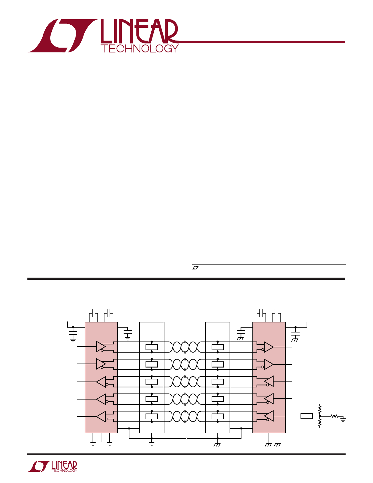
TYPICAL APPLICATIO
1µF
1µF 1µF1µF
V
CC1
5V
1µF
11
12
13
2
4
1
LTC1345 LTC1345
6
DX
7
DX
RX
RX
RX
10
14
9
V
CC1
The transceiver operates up to 10Mbaud. All transmitters
feature short-circuit protection and a Receiver Output
Enable pin allows the receiver outputs to be forced into a
high impedance state. Both transmitter outputs and receiver inputs feature ±10kV ESD protection. The charge
pump features a regulated VEE output using three external
1µF capacitors.
, LTC and LT are registered trademarks of Linear Technology Corporation.
U
Clock and Data Signals for V.35 Interface
DCEDTE
28
273
26
25
24
23
20
19
18
17
16
15
5
1µF
1
2
3
4
14
13
12
11
10
9
7
BI
627T500/1250
T
T T
T T
T T
T T
8
TXD (103)
SCTE (113)
TXC (114)
RXC (115)
RXD (104)
GND (102)
BI
627T500/1250
T
8
12
111817
10
9
1
2
3
4
5
6
7
1µF
16
15
26
25
24
23
22
21
1
28
2
4
RX
RX
DX
DX
DX
5
10 14
9
V
CC2
V
327
1µF
12
13
6
7
8
627T500/1250 (SOIC) OR
LTC1345 • TA01
CC2
5V
50Ω
=
T
50Ω
BI TECHNOLOGIES
899TR50/125 (DIP)
125Ω
1
LTC1345
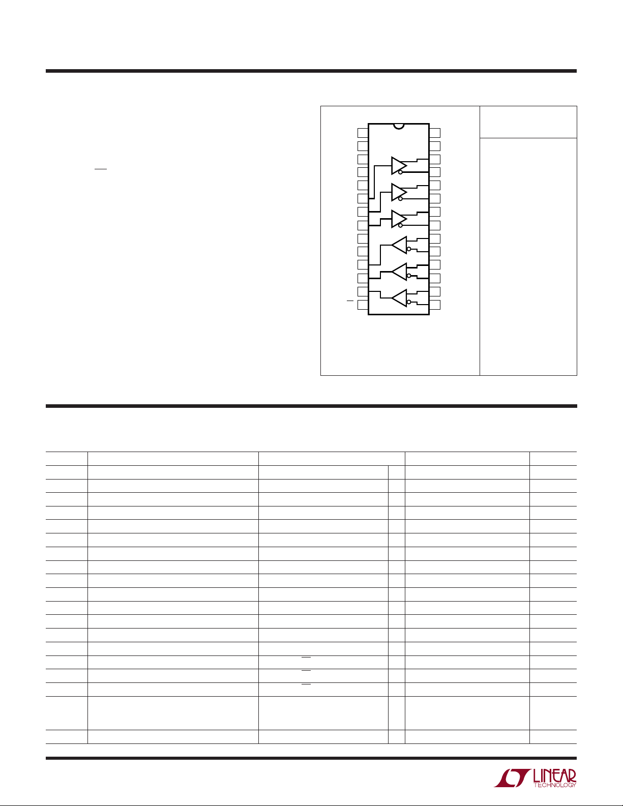
PACKAGE/ORDER I FOR ATIO
UU
W
WWWU
ABSOLUTE AXI U RATI GS
(Note 1)
Supply Voltage, VCC.................................................. 6V
Input Voltage
Transmitters ........................... –0.3V to (VCC + 0.3V)
Receivers............................................... –18V to 18V
S1, S2, OE ............................... –0.3V to (VCC + 0.3V)
Output Voltage
Transmitters .......................................... –18V to 18V
Receivers................................ –0.3V to (VCC + 0.3V)
VEE........................................................ –10V to 0.3V
Short-Circuit Duration
Transmitter Output ..................................... Indefinite
Receiver Output.......................................... Indefinite
VEE................................................................. 30 sec
Operating Temperature Range
Commercial ............................................ 0°C to 70°C
Industrial ........................................... – 40°C to 85°C
Storage Temperature Range ................ – 65°C to 150°C
Lead Temperature (Soldering, 10 sec)................. 300°C
TOP VIEW
+
1
C2
+
2
C1
3
V
CC
–
4
C1
5
GND
6
T1
7
T2
8
T3
9
S1
10
S2
11
R3
12
R2
13
R1
14
OE
NW PACKAGE
28-LEAD PDIP
THREE V.35 TRANSMITTERS AND THREE RECEIVERS
T
= 125°C, θ
JMAX
T
= 125°C, θ
JMAX
SW PACKAGE
28-LEAD PLASTIC SO
= 56°C/W (NW)
JA
= 65°C/W (SW)
JA
–
28
C2
27
V
EE
26
Y1
25
Z1
24
Y2
23
Z2
22
Y3
21
Z3
20
B3
19
A3
18
B2
17
A2
16
B1
15
A1
ORDER PART
NUMBER
LTC1345CNW
LTC1345CSW
LTC1345INW
LTC1345ISW
Consult factory for Military grade parts.
DC ELECTRICAL CHARACTERISTICS
The ● denotes specifications which apply over the full operating
temperature range, otherwise specifications are at TA = 25°C. VCC = 5V ±5% (Notes 2, 3), unless otherwise specified.
SYMBOL PARAMETER CONDITIONS MIN TYP MAX UNITS
V
V
I
OH
I
OL
I
OZ
R
V
∆V
I
IN
R
V
V
I
OSR
I
OZR
V
V
I
IN
I
CC
V
OD
OC
O
TH
TH
IN
OH
OL
IH
IL
EE
Transmitter Differential Output Voltage Figure 1, –4V ≤ VOS ≤ 4V ● 0.44 0.55 0.66 V
Transmitter Common-Mode Output Voltage Figure 1, VOS = 0V ● –0.6 0 0.6 V
Transmitter Output High Current V
Transmitter Output Low Current V
Transmitter Output Leakage Current S1 = S2 = 0V, –5V ≤ V
Transmitter Output Impedance –2V ≤ V
= 0V ● –12.6 –11 – 9.4 mA
Y, Z
= 0V ● 9.4 11 12.6 mA
Y, Z
≤ 5V ● ±1 ±100 µA
Y, Z
≤ 2V 100 kΩ
Y, Z
Differential Receiver Input Threshold Voltage –7V ≤ (VA + VB)/2 ≤ 7V ● 25 200 mV
Receiver Input Hysterisis –7V ≤ (VA + VB)/2 ≤ 7V 50 mV
Receiver Input Current (A, B) –7V ≤ V
Receiver Input Impedance –7V ≤ V
Receiver Output High Voltage IO = 4mA, V
Receiver Output Low Voltage IO = 4mA, V
Receiver Output Short-Circuit Current 0V ≤ VO ≤ V
Receiver Three-State Output Current S1 = S2 = 0V, 0V ≤ VO ≤ V
≤ 7V ● 0.4 mA
A, B
≤ 7V ● 17.5 30 kΩ
A, B
= 0.2V ● 3 4.5 V
B, A
= –0.2V ● 0.2 0.4 V
B, A
CC
CC
● 785mA
● ±10 µA
Logic Input High Voltage T, S1, S2, OE ● 2V
Logic Input Low Voltage T, S1, S2, OE ● 0.8 V
Logic Input Current T, S1, S2, OE ● ±10 µA
VCC Supply Current Figure 1, VOS = 0, S1 = S2 = HIGH ● 118 170 mA
No Load, S1 = S2 = HIGH
Shutdown, S1 = S2 = 0V
● 19 30 mA
● 1 100 µA
VEE Voltage No Load, S1 = S2 = HIGH –5.5 V
2
LTC1345
TEMPERATURE (˚C)
–50
TIME (ns)
25
LTC1345 • TPC03
10
5
–25 0 50
0
20
15
75 100 125
VCC = 5V
AC ELECTRICAL CHARACTERISTICS
The ● denotes specifications which apply over the full operating
temperature range, otherwise specifications are at TA = 25°C. VCC = 5V ±5% (Notes 2, 3), unless otherwise specified.
SYMBOL PARAMETER CONDITIONS MIN TYP MAX UNITS
tR, t
F
t
PLH
t
PHL
t
SKEW
t
PLH
t
PHL
t
SKEW
t
ZL
t
ZH
t
LZ
t
HZ
f
OSC
BR
MAX
Note 1: The absolute maximum ratings are those values beyond which the
safety of the device cannot be guaranteed.
Note 2: All currents into device pins are termed positive; all currents out of
device pins are termed negative. All voltages are referenced to device
ground unless otherwise specified.
Transmitter Rise or Fall Time Figures 1 and 3, VOS = 0V ● 740 ns
Transmitter Input to Output Figures 1 and 3, VOS = 0V ● 25 70 ns
Transmitter Input to Output Figures 1 and 3, VOS = 0V ● 25 70 ns
Transmitter Output to Output Figures 1 and 3, VOS = 0V 0 ns
Receiver Input to Output Figures 1 and 4, VOS = 0V ● 49 100 ns
Receiver Input to Output Figures 1 and 4, VOS = 0V ● 52 100 ns
Differential Receiver Skew, t
PLH
– t
PHL
Figures 1 and 4, VOS = 0V 3 ns
Receiver Enable to Output LOW Figures 2 and 5, CL = 15pF, S1 Closed ● 40 70 ns
Receiver Enable to Output HIGH Figures 2 and 5, CL = 15pF, S2 Closed ● 35 70 ns
Receiver Disable From LOW Figures 2 and 5, CL = 15pF, S1 Closed ● 30 70 ns
Receiver Disable From HIGH Figures 2 and 5, CL = 15pF, S2 Closed ● 35 70 ns
Charge Pump Oscillator Frequency 200 kHz
Maximum Data Rate (Note 4) ● 10 15 Mbaud
Note 3: All typicals are given for VCC = 5V, C1 = C2 = C3 = 1µF ceramic
capacitors and T
= 25°C.
A
Note 4: Maximum data rate is specified for NRZ data encoding scheme.
The maximum data rate may be different for other data encoding schemes.
Data rate is guaranteed by correlation and is not tested.
UW
TYPICAL PERFOR A CE CHARACTERISTICS
Transmitter Output Current
vs Output Voltage
13
TA = 25°C
= 5V
V
CC
12
11
10
OUTPUT CURRENT (mA)
9
–1.5
–2.0
–0.5
–1.0
OUTPUT VOLTAGE (V)
OUTPUT CURRENT (mA)
Transmitter Output Current
vs Temperature
13
VCC = 5V
12
11
10
9
–25 0 50
–50
25
TEMPERATURE (˚C)
75 100 125
LTC1345 • TPC01
Transmitter Output Skew
vs Temperature
0.5
0
1.0
1.5
LTC1345 • TPC02
2.0
3
LTC1345
TEMPERATURE (˚C)
–50
VOLTAGE (V)
25
LTC1345 • TPC06
–5.5
–6.0
–25 0 50
–6.5
–4.5
–5.0
75 100 125
VCC = 5V
UW
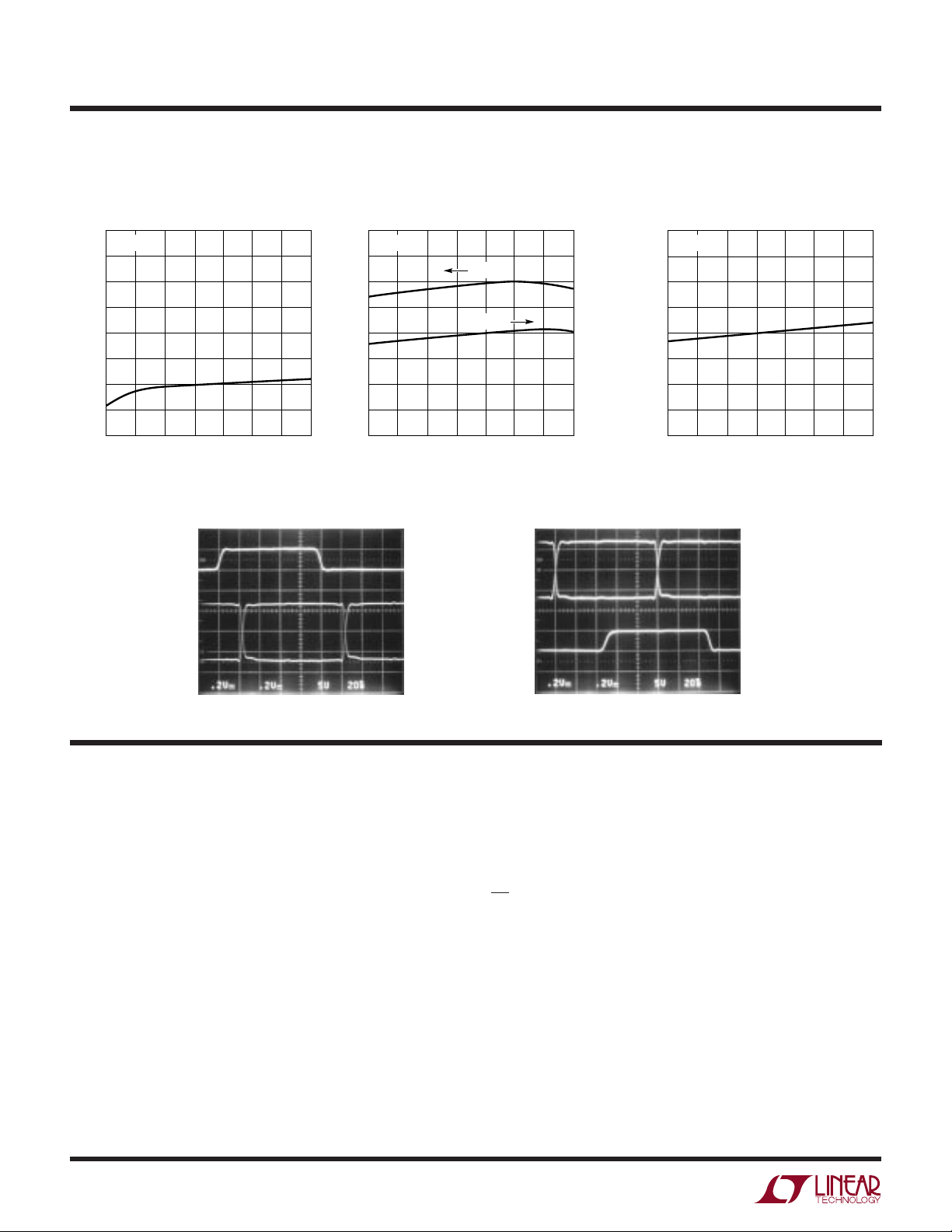
TYPICAL PERFOR A CE CHARACTERISTICS
Receiver t
vs Temperature
20
VCC = 5V
15
10
TIME (ns)
5
0
–25 0 50
–50
– t
PLH
TEMPERATURE (˚C)
PHL
25
75 100 125
LTC1345 • TPC04
Transmitter Output Waveforms
INPUT
5V/DIV
OUTPUT
0.2V/DIV
Supply Current vs Temperature
140
VCC = 5V
120
100
CURRENT (mA)
80
60
–25 0 50
–50
LOADED
NO LOAD
25
TEMPERATURE (˚C)
30
25
CURRENT (mA)
20
15
75 100 125
LTC1345 • TPC05
10
Receiver Output Waveforms
INPUT
0.2/DIV
OUTPUT
5V/DIV
VEE Voltage vs Temperature
LTC1345 • TPC07
U
UU
PI FU CTIO S
C2+ (Pin 1):
C1+ (Pin 2): Capacitor C1 Positive Terminal.
VCC (Pin 3): Positive Supply, 4.75 ≤ VCC ≤ 5.25V.
C1– (Pin 4): Capacitor C1 Negative Terminal.
GND (Pin 5): Ground. The positive terminal of C3 is
connected to ground.
T1 (Pin 6): Transmitter 1 Input.
T2 (Pin 7): Transmitter 2 Input.
T3 (Pin 8): Transmitter 3 Input.
S1 (Pin 9): Select Input 1.
S2 (Pin 10): Select Input 2.
Capacitor C2 Positive Terminal.
LTC1345 • TPC08
R3 (Pin 11): Receiver 3 Output.
R2 (Pin 12): Receiver 2 Output.
R1 (Pin 13): Receiver 1 Output.
OE (Pin 14): Receiver Output Enable.
A1 (Pin 15): Receiver 1 Inverting Input.
B1 (Pin 16): Receiver 1 Noninverting Input.
A2 (Pin 17): Receiver 2 Inverting Input.
B2 (Pin 18): Receiver 2 Noninverting Input.
A3 (Pin 19): Receiver 3 Inverting Input.
B3 (Pin 20): Receiver 3 Noninverting Input.
Z3 (Pin 21): Transmitter 3 Inverting Output.
4
 Loading...