

Linear Technology LTC1343 Datasheet
FEATURES
■
Software-Selectable Transceiver Supports:
RS232, RS449, EIA-530, EIA-530-A, V.35, V.36,
X.21
■
NET1 and NET2 Compliant
■
Software-Selectable Cable Termination Using
the LTC1344
■
4-Driver/4-Receiver Configuration Provides a
Complete 2-Chip DTE or DCE Port
■
Operates from Single 5V Supply
■
Internal Echoed Clock and Loop-Back Logic
U
APPLICATIO S
■
Data Networking
■
CSU and DSU
■
Data Routers
, LTC and LT are registered trademarks of Linear Technology Corporation.
LTC1343
Software-Selectable
Multiprotocol Transceiver
U
DESCRIPTIO
The LTC®1343 is a 4-driver/4-receiver multiprotocol transceiver that operates from a single 5V supply. Two LTC1343s
form the core of a complete software-selectable DTE or DCE
interface port that supports the RS232, RS449, EIA-530,
EIA-530-A, V.35, V.36 or X.21 protocols. Cable termination
may be implemented using the LTC1344 software-selectable
cable termination chip or by using existing discrete designs.
The LTC1343 runs from a single 5V supply using an internal
charge pump that requires only five space saving surface mount
capacitors. The mode pins are latched internally to allow sharing
of the select lines between multiple interface ports.
Software-selectable echoed clock and loop-back modes help
eliminate the need for external glue logic between the serial
controller and line transceiver. The part features a flowthrough architecture to simplify EMI shielding and is available
in the 44-lead SSOP surface mount package.
TYPICAL APPLICATIO
LTC1343
DSR A (107)
DSR B
R1
DCD A (109)
DCD B
DTR B
R3R4R2
CTS A (106)
CTS B
U
DTE Multiprotocol Serial Interface with DB-25 Connector
RTSDTRDSR DCDCTS RL
LTC1343
D1
D2
D3D4
DTR A (108)
RTS B
RL A (140)
RTS A (105)
TM A (142)
SGND (102)
SHIELD (101)
R3R4R2
RXD A (104)
RXD B
RXC A (115)
RXC B
R1
TXC A (114)
TXC B
D3D4
SCTE B
TXDSCTETXCRXCRXDTM
D2
TXD A (103)
TXD B
SCTE A (113)
21424111512179314192023622 810513 21 7 1625
LL
D1
18
LL A (141)
LTC1344
DB-25 CONNECTOR
1343 TA01
1
LTC1343
WW
W
U
ABSOLUTE MAXIMUM RATINGS
(Note 1)
Supply Voltage ....................................................... 6.5V
Input Voltage
Transmitters ........................... –0.3V to (VCC + 0.3V)
Receivers............................................... –18V to 18V
Logic Pins .............................. –0.3V to (VCC + 0.3V)
Output Voltage
Transmitters ................. (VEE – 0.3V) to (VDD + 0.3V)
Receivers................................ –0.3V to (VCC + 0.3V)
Logic Pins .............................. –0.3V to (VCC + 0.3V)
VEE........................................................ –10V to 0.3V
VDD....................................................... –0.3V to 10V
Short-Circuit Duration
Transmitter Output ..................................... Indefinite
Receiver Output.......................................... Indefinite
VEE.................................................................. 30 sec
Operating Temperature Range
LTC1343C .............................................. 0°C to 70°C
LTC1343I........................................... –40°C to 85°C
Storage Temperature Range ................ –65°C to 150°C
Lead Temperature (Soldering, 10 sec)................. 300°C
U
W
PACKAGE/ORDER INFORMATION
V
C1
PWRV
C1
V
D4EN
INVERT
R1EN
R1O
R2O
R3O
R4O
CTRL/CLK
DCE/DTE
LATCH
TOP VIEW
1
DD
+
2
CHARGE PUMP
3
CC
–
4
5
D1
6
D2
7
D3
8
CC
9
D4
10
11
12
13
14
15
16
17
M0
18
M1
19
M2
20
21
22
T
JMAX
D1
D2
D3
D4
R1
R2
R3
R4
GW PACKAGE
44-LEAD PLASTIC SSOP
= 150°C, θJA = 65°C/W
44
43
42
41
40
39
38
37
36
35
34
33
32
31
30
29
28
27
26
25
24
23
+
C2
–
C2
V
EE
PGND
GND
D1 A
D2 A
D2 B
D3 A
D3 B
D4 A
D4 B
R1 A
R1 B
R2 A
R2 B
R3 A
R3 B
R4 A
423 SET
EC
LB
ORDER PART
NUMBER
LTC1343CGW
LTC1343IGW
U
Consult factory for Military grade parts.
ELECTRICAL CHARACTERISTICS
temperature range, otherwise specifications are at T
The ● denotes specifications which apply over the full operating
= 25°C. V
A
= 5V (Notes 2, 3)
CC
SYMBOL PARAMETER CONDITIONS MIN TYP MAX UNITS
Supplies
I
CC
VCC Supply Current (DCE Mode, V.10 Mode, No Load 12 mA
All Digital Pins = GND or V
) V.10 Mode, Full Load ● 80 150 mA
CC
RS530, RS530-A, X.21 Modes, No Load 80 mA
RS530, RS530-A, X.21 Modes, Full Load
● 160 200 mA
V.35 Mode, No Load 20 mA
V.35 Mode, Full Load
● 115 160 mA
V.28 Mode, No Load 20 mA
V.28 Mode, Full Load
No-Cable Mode
P
D
Internal Power Dissipation (DCE Mode, V.10 Mode, Full Load 400 mW
All Digital Pins = GND or V
) RS530, RS530-A, X.21 Modes, Full Load 680 mW
CC
● 30 90 mA
● 0.05 1 mA
V.35 Mode, Full Load 500 mW
V.28 Mode, Full Load 150 mW
+
V
–
V
Positive Charge Pump Output Voltage Any Mode, No Load ● 8.5 9.1 V
V.28 Mode, with Load
● 8.0 7.0 V
Negative Charge Pump Output Voltage V.28 Mode, Full Load ● –7.8 – 8.4 V
V.35 Mode, Full Load ● – 5.8 –6.7 V
–40°C ≤ T
≤ 85°C ● – 5.5 V
A
V.10, RS530, RS530A, X.21 Modes, Full Load ● –5.0 – 6.1 V
–40°C ≤ TA ≤ 85°C ● – 4.8 V
2
LTC1343
ELECTRICAL CHARACTERISTICS
temperature range, otherwise specifications are at T
The ● denotes specifications which apply over the full operating
= 25°C. V
A
= 5V (Notes 2, 3)
CC
SYMBOL PARAMETER CONDITIONS MIN TYP MAX UNITS
t
r
Supply Rise Time No-Cable Mode or Power-Up to Turn On 2 ms
Logic Inputs and Outputs
V
V
I
IN
V
V
I
OSR
I
OZR
IH
IL
OH
OL
Logic Input High Voltage ● 2V
Logic Input Low Voltage ● 0.8 V
Logic Input Current ● ±10 µA
Output High Voltage IO = –4mA ● 3 4.5 V
Output Low Voltage IO = 4mA ● 0.3 0.8 V
Output Short-Circuit Current 0V ≤ VO ≤ VCC, 0°C ≤ TA ≤ 70°C ● –60 60 mA
≤ VCC, –40°C ≤ TA ≤ 85°C ● –70 70 mA
0V ≤ V
O
Three-State Output Current M0 = M1 = M2 = VCC, 0V ≤ VO ≤ V
CC
±1 µA
V.11 Driver
V
OD
Differential Output Voltage Open Circuit, RL = 1.95k ● ±6V
= 50Ω (Figure 1), ● ±2V
R
L
VOD at 50Ω > 1/2 VOD at RL = 1.95k
∆V
OD
Change in Magnitude of Differential RL = 50Ω (Figure 1) ● 0.2 V
Output Voltage
V
∆V
OC
OC
Common Mode Output Voltage RL = 50Ω (Figure 1) ● 3.0 V
Change in Magnitude of Common Mode RL = 50Ω (Figure 1) ● 0.2 V
Output Voltage
I
SS
Short-Circuit Current –0.25V ≤ VO ≤ 0.25V, Power Off or ±150 mA
No-Cable Mode or Driver Disabled
I
OZ
Output Leakage Current –0.25V ≤ VO ≤ 0.25V, Power Off or ● ±0.01 ±100 µA
No-Cable Mode or Driver Disabled
tr, t
f
t
PLH
t
PHL
∆t Input to Output Difference, t
t
SKEW
Rise or Fall Time (Figures 2, 6) ● 41325 ns
Input to Output (Figures 2, 6), 0°C ≤ TA ≤ 70°C ● 25 55 80 ns
(Figures 2, 6), –40°C ≤ T
≤ 85°C ● 25 55 90 ns
A
Input to Output (Figures 2, 6), 0°C ≤ TA ≤ 70°C ● 25 55 80 ns
≤ 85°C ● 25 55 90 ns
A
≤ 70°C ● 0317 ns
A
≤ 85°C ● 0325 ns
A
PLH
(Figures 2, 6), –40°C ≤ T
– t
(Figures 2, 6), 0°C ≤ T
PHL
(Figures 2, 6), –40°C ≤ T
Output to Output Skew (Figures 2, 6) 3 ns
V.11 Receiver
V
∆V
I
IN
R
tr, t
t
PLH
TH
TH
IN
f
Input Threshold Voltage –7V ≤ VCM ≤ 7V, 0°C ≤ TA ≤ 70°C ● – 0.2 0.2 V
–7V ≤ V
≤ 7V, –40°C ≤ TA ≤ 85°C ● – 0.3 0.3 V
CM
Input Hysteresis –7V ≤ VCM ≤ 7V, 0°C ≤ TA ≤ 70°C ● 15 40 mV
–7V ≤ V
Input Current (A, B) –10V ≤ V
Input Impedance –10V ≤ V
≤ 7V, –40°C ≤ TA ≤ 85°C ● 60 mV
CM
≤ 10V ● ±0.50 mA
A, B
≤ 10V ● 20 32 kΩ
A, B
Rise or Fall Time (Figures 2, 7) 15 ns
Input to Output (Figures 2, 7), CTRL = GND, 0°C ≤ TA ≤ 70°C ● 35 80 115 ns
CTRL = V
, 0°C ≤ TA ≤ 70°C 400 ns
CC
(Figures 2, 7), CTRL = GND, –40°C ≤ TA ≤ 85°C ● 25 80 130 ns
CTRL = V
, –40°C ≤ TA ≤ 85°C 400 ns
CC
3
LTC1343
ELECTRICAL CHARACTERISTICS
temperature range, otherwise specifications are at T
The ● denotes specifications which apply over the full operating
= 25°C. V
A
= 5V (Notes 2, 3)
CC
SYMBOL PARAMETER CONDITIONS MIN TYP MAX UNITS
t
PHL
Input to Output (Figures 2, 7), CTRL = GND, 0°C ≤ TA ≤ 70°C ● 35 80 115 ns
CTRL = V
, 0°C ≤ TA ≤ 70°C 400 ns
CC
(Figures 2, 7), CTRL = GND, –40°C ≤ TA ≤ 85°C ● 25 80 130 ns
, –40°C ≤ TA ≤ 85°C 400 ns
CC
≤ 70°C ● 0517 ns
A
≤ 85°C ● 0525 ns
A
∆t Input to Output Difference, t
PLH
CTRL = V
– t
(Figures 2, 7), 0°C ≤ T
PHL
(Figures 2, 7), –40°C ≤ T
V.35 Driver
V
I
OH
I
OL
I
OZ
tr, t
t
PLH
OD
f
Differential Output Voltage Open Circuit 6.0 V
With Load, –4.0V ≤ V
Transmitter Output High Current V
Transmitter Output Low Current V
= 0V ● –12.6 – 11 –9.4 mA
A, B
= 0V ● 9.4 11 12.6 mA
A, B
Transmitter Output Leakage Current –0.25V ≤ V
≤ 0.25V ● ±0.01 ±100 µA
A, B
= 4.0V (Figure 3) ● ±0.44 ±0.55 ±0.66 V
CM
Rise or Fall Time (Figures 3, 6) 5 ns
Input to Output (Figures 3, 6), 0°C ≤ TA ≤ 70°C ● 25 45 75 ns
(Figures 3, 6), –40°C ≤ TA ≤ 85°C ● 25 45 90 ns
t
PHL
Input to Output (Figures 3, 6), 0°C ≤ TA ≤ 70°C ● 25 45 75 ns
(Figures 3, 6), –40°C ≤ TA ≤ 85°C ● 25 45 90 ns
∆t Input to Output Difference, t
PLH
– t
(Figures 3, 6), 0°C ≤ T
PHL
≤ 70°C ● 0517 ns
A
(Figures 3, 6), –40°C ≤ TA ≤ 85°C ● 0525 ns
t
SKEW
Output to Output Skew (Figures 3, 6) 4 ns
V.35 Receiver
V
TH
Differential Receiver Input – 2V ≤ (VA + VB)/2 ≤ 2V (Figure 3) ● –0.2 0.2 V
Threshold Voltage
∆V
I
IN
R
tr, t
t
PLH
TH
IN
f
Receiver Input Hysteresis –2V ≤ (VA + VB)/2 ≤ 2V (Figure 3) ● 11 40 mV
Receiver Input Current (A, B) –10V ≤ V
Receiver Input Impedance –10V ≤ V
≤ 10V ● ±0.50 mA
A, B
≤ 10V ● 20 32 kΩ
A, B
Rise or Fall Time (Figures 3, 7) 15 ns
Input to Output (Figures 3, 7), 0°C ≤ TA ≤ 70°C ● 80 115 ns
(Figures 3, 7), –40°C ≤ TA ≤ 85°C ● 80 130 ns
t
PHL
Input to Output (Figures 3, 7), 0°C ≤ TA ≤ 70°C ● 100 115 ns
(Figures 3, 7), –40°C ≤ TA ≤ 85°C ● 100 130 ns
∆t Input to Output Difference, t
PLH
– t
(Figures 3, 7), 0°C ≤ T
PHL
≤ 70°C ● 417 ns
A
(Figures 3, 7), –40°C ≤ TA ≤ 85°C ● 425 ns
V.10 Driver
V
O
Output Voltage Open Circuit, RL = 3.9k ±4.0 ±6.0 V
= 450Ω (Figure 4) ±3.6 V
R
L
at 450Ω > 0.9 VO at RL = 3.9k
V
O
Driver 1 Only
I
SS
I
OZ
Short-Circuit Current VO = GND; EIA-530, X.21, EIA-530-A Modes ±150 mA
Output Leakage Current –0.25V ≤ VO ≤ 0.25V, Power Off or ● ±0.1 ±100 µA
No-Cable Mode or Driver Disabled
tr, t
t
PLH
t
PHL
f
Rise or Fall Time (Figures 4, 8), RL = 450Ω, CL = 100pF
R
= 100k 4 µs
423SET
Input to Output (Figures 4, 8), RL = 450Ω, CL = 100pF
R
= 100k 8 µs
423SET
Input to Output (Figures 4, 8), RL = 450Ω, CL = 100pF
R
= 100k 8 µs
423SET
4
LTC1343
ELECTRICAL CHARACTERISTICS
temperature range, otherwise specifications are at T
SYMBOL PARAMETER CONDITIONS MIN TYP MAX UNITS
V.10 Receiver
V
TH
∆V
TH
I
IN
R
IN
tr, t
f
t
PLH
t
PHL
V.28 Driver
V
O
I
SS
I
OZ
SR Slew Rate (Figures 4, 8), RL = 3k, CL = 2500pF ● 4.0 30.0 V/µs
t
PLH
t
PHL
V.28 Receiver
V
THL
V
TLH
∆V
TH
R
IN
tr, t
f
t
PLH
t
PHL
Receiver Input Threshold Voltage 0°C ≤ TA ≤ 70°C ● –0.2 0.2 V
Receiver Input Hysteresis ● 11 50 mV
Receiver Input Current –10V ≤ VA ≤ 10V ● ±0.50 mA
Receiver Input Impedance –10V ≤ VA ≤ 10V ● 20 30 kΩ
Rise or Fall Time (Figures 5, 9) 15 ns
Input to Output (Figures 5, 9) 350 ns
Input to Output (Figures 5, 9) 350 ns
Output Voltage Open Circuit ±10 V
Short-Circuit Current VO = GND ● ±150 mA
Output Leakage Current –0.25V ≤ VO ≤ 0.25V, Power Off or ● ±0.01 ±100 µA
Input to Output (Figures 4, 8), RL = 3k, CL = 2500pF ● 1.6 2.5 µs
Input to Output (Figures 4, 8), RL = 3k, CL = 2500pF ● 1.6 2.5 µs
Input Low Threshold Voltage ● 1.4 0.8 V
Input High Threshold Voltage ● 2.0 1.4 V
Receiver Input Hysteresis ● 0.1 0.4 1.0 V
Receiver Input Impedance –15V ≤ VA ≤ 15V ● 357 kΩ
Rise or Fall Time (Figures 5, 9) 15 ns
Input to Output (Figures 5, 9), CTRL = 0V 110 ns
Input to Output (Figures 5, 9), CTRL = 0V 170 ns
The ● denotes specifications which apply over the full operating
= 25°C. V
A
–7V ≤ V
= 3k (Figure 4) ● ±5 7.6 V
R
L
No-Cable Mode or Driver Disabled
CTRL = V
CTRL = V
= 5V (Notes 2, 3)
CC
≤ 7V, –40°C ≤ TA ≤ 85°C ● –0.3 0.3 V
CM
CC
CC
● 330 800 ns
● 480 800 ns
Note 1: Absolute Maximum Ratings are those beyond which the safety of a
device may be impaired.
Note 2: All currents into device pins are positive; all currents out of device
are negative. All voltages are referenced to device ground unless otherwise
specified.
UUU
PIN FUNCTIONS
VDD (Pin 1): Generated Positive Supply Voltage for
RS232. Connect a 1µF capacitor to ground.
C1+ (Pin 2): Capacitor C1 Positive Terminal. Connect a
1µF capacitor between C1+ and C1–.
PWRVCC (Pin 3): Positive Supply for the Charge Pump.
4.75V ≤ PWRVCC ≤ 5.25V. Tie to VCC (Pin 8) and bypass
with a 1µF capacitor to ground.
Note 3: All typicals are given for V
C
= 3.3µF tantalum capacitors and TA = 25°C.
VEE
= 5V, C1 = C2 = C
CC
VCC
= C
VDD
= 1µF,
C1–␣ (Pin 4): Capacitor C1 Negative Terminal.
D1 (Pin 5): TTL Level Driver 1 Input.
D2 (Pin 6): TTL Level Driver 2 Input.
D3 (Pin 7): TTL Level Driver 3 Input. Becomes a CMOS
level output when the chip is in the echoed clock mode
(EC = 0V).
5

LTC1343
UUU
PIN FUNCTIONS
V
(Pin 8): Positive Supply for the Transceivers. 4.75V ≤
CC
VCC ≤ 5.25V. Tie to PWRVCC (Pin 3).
respective input buffers. The data latch allows the logic
lines to be shared between multiple I/O ports.
D4 (Pin 9): TTL Level Driver 4 Input.
D4EN (Pin 10): TTL Level Enable Input for Driver 4. When
high, driver 4 outputs are enabled. When low, driver 4
outputs are forced into a high impedance state. D4EN is
not affected by the LATCH pin.
INVERT (Pin 11): TTL Level Signal Invert Input. When
high, an extra inverter will be added to the driver 4 and
receiver 1 signal path. The data stream will change polarity, i.e., a 1 becomes 0 and a 0 becomes a 1. When the pin
is low the data flows through with no polarity change.
INVERT is not affected by the LATCH pin.
R1EN (Pin 12): Logic Level Enable Input for Receiver 1.
When low, receiver 1 output is enabled. When high,
receiver 1 output is forced into a high impedance state.
R1O (Pin 13): CMOS Level Receiver 1 Output.
R2O (Pin 14): CMOS Level Receiver 2 Output.
R3O (Pin 15): CMOS Level Receiver 3 Output.
R4O (Pin 16): CMOS Level Receiver 4 Output.
M0 (Pin 17): TTL Level Mode Select Input 0. The data on
M0 is latched when LATCH is high.
LB (Pin 23): TTL Level Loop-Back Select Input. When low
the chip enters the loop-back configuration and is configured for normal operation when LB is high. The data on LB
is latched when LATCH is high.
EC (Pin 24): TTL Level Echoed Clock Select Input. When
low the part enters the echoed clock configuration and is
configured for normal operation when EC is high. The data
on EC is latched when LATCH is high.
423 SET (Pin 25): Analog Input Pin for the RS423 Driver
Output Rise and Fall Time Set Resistor. Connect the
resistor from the pin to ground.
R4 A (Pin 26): Receiver 4 Inverting Input.
R3 B (Pin 27): Receiver 3 Noninverting Input.
R3 A (Pin 28): Receiver 3 Inverting Input.
R2 B (Pin 29): Receiver 2 Noninverting Input.
R2 A (Pin 30): Receiver 2 Inverting Input.
R1 B (Pin 31): Receiver 1 Noninverting Input.
R1 A (Pin 32): Receiver 1 Inverting Input.
D4 B (Pin 33): Driver 4 Noninverting Output.
M1 (Pin 18): TTL Level Mode Select Input 1. The data on
M1 is latched when LATCH is high.
M2 (Pin 19): TTL Level Mode Select Input 2. The data on
M2 is latched when LATCH is high.
CTRL/CLK (Pin 20): TTL Level Mode Select Input. When
the pin is low the chip will be configured for clock and data
signals. When the pin is high the chip will be configured for
control signals. The data on CTRL/CLK is latched when
LATCH is high.
DCE/DTE (Pin 21): TTL Level Mode Select Input. When
high, the DCE mode is selected. When low the DTE mode
is selected. The data on DCE/DTE is latched when LATCH
is high.
LATCH (Pin 22): TTL Level Logic Signal Latch Input. When
low the input buffers on M0, M1, M2, CTRL/CLK, DCE/
DTE, LB and EC are transparent. When LATCH is pulled
high the data on the logic pins is latched into their
D4 A (Pin 34): Driver 4 Inverting Output.
D3 B (Pin 35): Driver 3 Noninverting Output.
D3 A (Pin 36): Driver 3 Inverting Output.
D2 B (Pin 37): Driver 2 Noninverting Output.
D2 A (Pin 38): Driver 2 Inverting Output.
D1 A (Pin 39): Driver 1 Inverting Output.
GND (Pin 40): Signal Ground. Connect to PGND (Pin 41).
PGND (Pin 41): Charge Pump Power Ground. Connect to
the GND (Pin 40).
VEE (Pin 42): Generated Negative Supply Voltage. Connect
a 3.3µF capacitor to ground.
C2– (Pin 43): Capacitor C2 Negative Terminal. Connect a
1µF capacitor between C2+ and C2–.
C2+ (Pin 44): Capacitor C2 Positive Terminal. Connect a
1µF capacitor between C2+ and C2–.
6
TEST CIRCUITS
A
V
OD
B
Figure 1. RS422 Driver Test Circuit Figure 2. RS422 Driver/Receiver AC Test Circuit
R
L
50Ω
R
L
50Ω
LTC1343
C
L
B
R
L
100Ω
A
V
OC
1343 F01
100pF
C
100pF
B
R
L
A
15pF
1343 F02
B
D
V
A
50Ω
125Ω
OD
50Ω
V
CM
125Ω
50Ω
50Ω
B
R
A
15pF
1343 F03
Figure 3. V.35 Driver/Receiver Test Circuit
D
A
R
C
L
L
1343 F04
D
A
A
R
15pF
1343 F04
Figure 4. V.10/V.28 Driver Test Circuit Figure 5. V.10/V.28 Receiver Test Circuit
W
U
ODE SELECTIO
LTC1343 MODE NAME M2 M1 M0 CTRL/CLK D1 D2 D3 D4 R1 R2 R3 R4
V.10, RS423 0 0 0 X V.10 V.10 V.10 V.10 V.10 V.10 V.10 V.10
EIA-530-A Clock and Data 0 0 1 0 V.10 V.11 V.11 V.11 V.11 V.11 V.11 V.10
EIA-530-A Control 0 0 1 1 V.10 V.11 V.10 V.11 V.11 V.10 V.11 V.10
Reserved 0 1 0 X V.10 V.11 V.11 V.11 V.11 V.11 V.11 V.10
X.21 0 1 1 X V.10 V.11 V.11 V.11 V.11 V.11 V.11 V.10
V.35 Clock and Data 1 0 0 0 V.28 V.35 V.35 V.35 V.35 V.35 V.35 V.28
V.35 Control 1 0 0 1 V.28 V.28 V.28 V.28 V.28 V.28 V.28 V.28
EIA-530, RS449, V.36 1 0 1 X V.10 V.11 V.11 V.11 V.11 V.11 V.11 V.10
V.28, RS232 1 1 0 X V.28 V.28 V.28 V.28 V.28 V.28 V.28 V.28
No Cable 1 1 1 X Z Z Z Z Z Z Z Z
7
LTC1343
UWW
SWITCHI G TI E WAVEFOR S
B – A
B – A
–V
5V
D
0V
V
O
–V
O
A
B
V
O
1.5V 1.5V
t
PLH
50%
90%
10%
t
r
t
SKEW
f = 1MHz : tr ≤ 10ns : tf ≤ 10ns
= V(A) – V(B)
V
DIFF
1/2 V
O
t
PHL
90%
50%
10%
t
f
t
SKEW
1343 F06
Figure 6. V.11, V.35 Driver Propagation Delays
V
OD2
OD2
V
OH
R
V
OL
0V
t
PLH
1.5V
f = 1MHz : tr ≤ 10ns : tf ≤ 10ns
INPUT
OUTPUT
0V
t
PHL
1.5V
1343 F07
Figure 7. V.11, V.35 Receiver Propagation Delays
3V
D
0V
V
O
A
–V
O
1.5V
t
PHL
3V
0V
–3V
t
f
1.5V
–3V
t
PLH
0V
3V
t
r
1343 F08
8
Figure 8. V.10, V.28 Driver Propagation Delays
V
IH
A
V
IL
V
OH
R
V
OL
1.3V
t
PHL
0.8V
1.7V
t
PLH
2.4V
1343 F09
Figure 9. V.10, V.28 Receiver Propagation Delays
LTC1343
U
WUU
APPLICATIONS INFORMATION
Overview
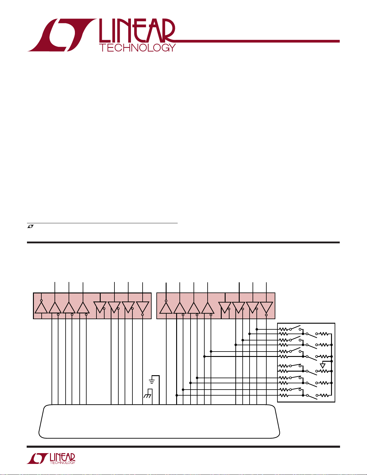
The LTC1343 is a 4-driver/4-receiver multiprotocol transceiver that operates from a single 5V supply. Two LTC1343s
form the core of a complete software-selectable DTE or
DCE interface port that supports the RS232, RS449,
EIA-530, EIA-530-A, V.35, V.36 or X.21 protocols. Cable
termination may be implemented using the LTC1344
SERIAL
CONTROLLER
TXD
SCTE
LL
LTC1343
D1
D2
D3
D4
TXD
SCTE
software-selectable cable termination chip or by using
existing discrete designs.
A complete DCE-to-DTE interface operating in EIA-530
mode is shown in Figure 10. The first LTC1343 of each port
is used to generate the clock and data signals along with
LL (Local Loop-back) and TM (Test Mode). The second
LTC1343 is used to generate the control signals along with
DCEDTE
LTC1343LTC1344 LTC1344
LL
103Ω
103Ω
R4
R3
R2
R1
SERIAL
CONTROLLER
LL
TXD
SCTE
TXC
RXC
RXD
TM
RL
RTS
DTR
DCD
DSR
R1
R2
R3
R4
LTC1343
D1
D2
D3
D4
R1
R2
103Ω
103Ω
103Ω
TXC
RXC
RXD
TM
RTS
DTR
DCD
DSR
D4
D3
D2
D1
RL
LTC1343
R4
R3
R2
R1
D4
D3
TXC
RXC
RXD
TM
RL
RTS
DTR
DCD
DSR
CTS
R3
RI
R4
CTS
RI
D2
D1
CTS
RI
1343 F10
Figure 10. Complete Multiprotocol Interface in EIA-530 Mode
9
 Loading...