

Application Note 64
Using the LTC1325 Battery Management IC
Anthony Ng, Peter Schwartz, Robert Reay,
Richard Markell
INTRODUCTION
August 1996
For a variety of reasons, it is desirable to charge batteries
as rapidly as possible. At the same time, overcharging
must be limited to prolong battery life. Such limitation of
overcharging depends on factors such as the choice of
charge termination technique and the use of multi-rate/
multi-stage charging schemes. The majority of battery
charger ICs available today lock the user into one fixed
charging regimen, with at best a limited number of
customization options to suit a variety of application needs
or battery types. The LTC®1325 addresses these shortcomings by providing the user with all the functional
blocks needed to implement a simple but highly flexible
battery charger (see Figure 1) which not only addresses
the issue of charging batteries but also those of battery
conditioning and capacity monitoring. A microprocessor
interacts with the LTC1325 through a serial interface to
control the operation of its functional blocks, allowing
software to expand the scope and flexibility of the charger
circuit.
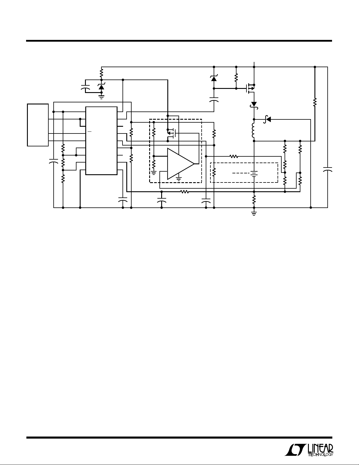
MPU
(e.g. 8051)
p1.4
p1.3
p1.2
REG
D
OUT
D
IN
CS
R1
10k
1%
C
REG
+
NOTE 1: THERMISTORS 1 AND 2 ARE PANASONIC ERT-D2FHL103S NTC THERMISTORS OR EQUIVALENT.
NOTE 2: V
NOTE 3: CHOOSE FOR C/20 TRICKLE CHARGE RATE.
NOTE 4: 2.0k AND 47µF FOR COMPATIBILITY WITH LITHIUM-ION AND LEAD-ACID
4.7µF
TANT
25V
R2
10k
1%
R3
10k
1%
= 160mV, R
REF
CLK
LTF
MCV
HTF
GND
SENSE
VDD
PGATE
DIS
LTC1325
V
BAT
T
BAT
T
AMB
V
IN
SENSE
FILTER
+
= 1 FOR C/3 CHARGE RATE (160mA).
C
1µF
F
R4
7.5k
1%
THERM 2
10k
NOTE 1
+ +
This Application Note was written with the following
objectives in mind :
• Provide users with an insight into the architecture and
operation of the LTC1325.
• Outline basic techniques for charging various battery
types.
• Present a variety of useful, tried and tested charging
circuits.
• Give an overview of the most common battery types
and their characteristics.
• Clarify specialized and application-specific terminology. Definitions are provided in the text, as well as in
Appendix C.
, LTC and LT are registered trademarks of Linear Technology Corporation.
V
DC
16V MAX
C2
+
R
AN64 F01
10µF
TANT
25V
500pF
3.3µF
(NOTE 4)
COILTRONICS
R5
7.5k
1%
100Ω (NOTE 4)
THERM 1
10k
NOTE 1
100Ω
CTX100-1-52
100µH
V
BAT
8 CELLS
500mA HR
C/3 RATE
P1
IRF9531
L1
D1
1N5818
IRF510
R
SENSE
1Ω
TRK
NOTE 3
R
DIS
N1
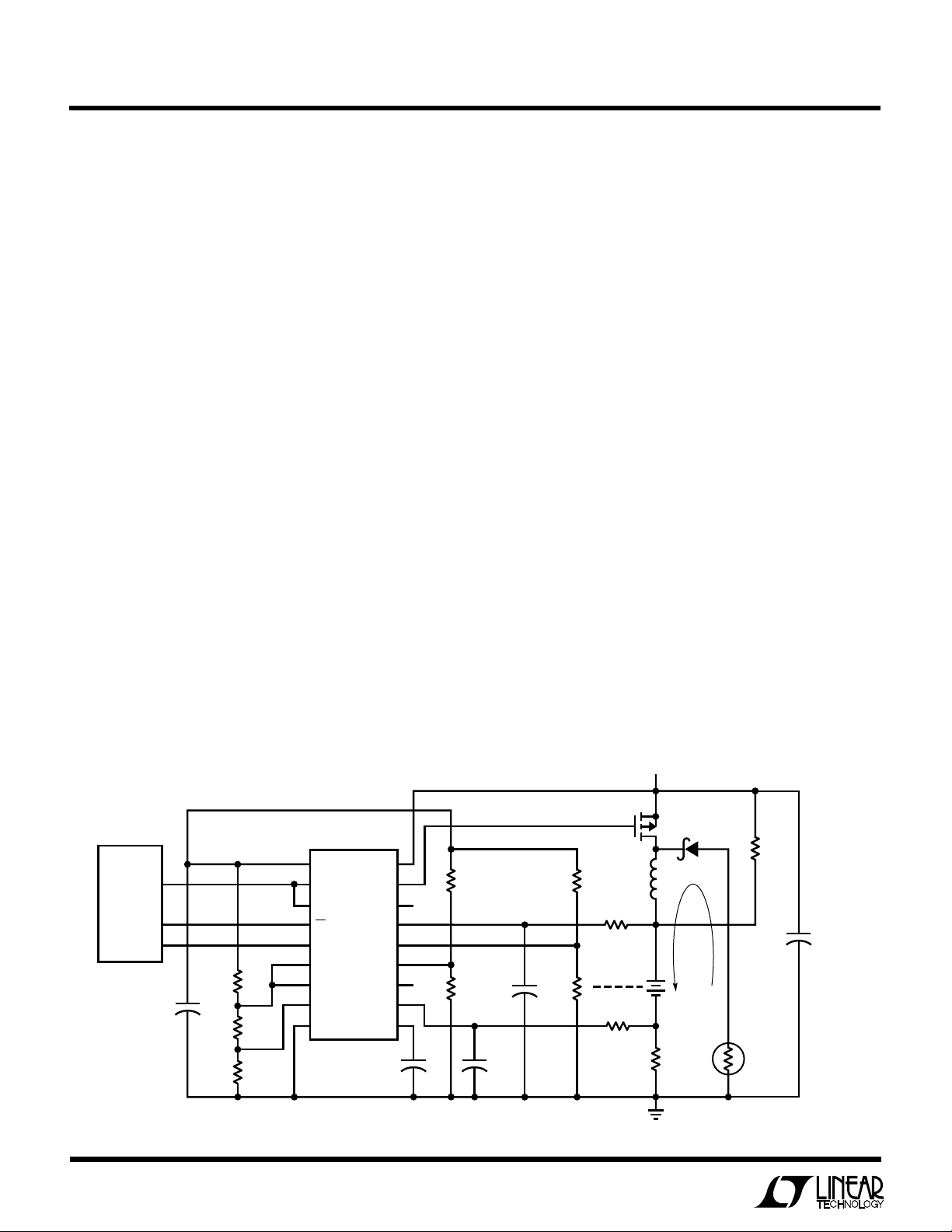
Figure 1. Complete LTC1325 Battery Management System
AN64-1

Application Note 64
LTC1325 PRIMER
The main features of the LTC1325 may be summarized as
follows:
• It has all the functional blocks needed to build a charger:
a 10-bit Analog-to-Digital Converter (ADC), fault detection circuitry, a switching regulator controller with a
MOSFET driver, a programmable timer, a precision
3.072V regulator for powering external temperature
sensors, and a programmable battery voltage divider.
• The functional blocks are placed under the control of an
external microprocessor for ready adaptability to
different charging algorithms, battery chemistries, or
charge rates.
• Communication with the microprocessor is via a simple
serial interface, configurable for 3-wire or 4-wire operation.
• It has autonomous fault detection circuitry to protect
the battery against temperature or voltage extremes.
• In addition to charging, the part can discharge batteries
for battery conditioning purposes.
• It includes on-chip circuitry for an accurate battery
capacity monitor (Gas Gauge).
• It charges batteries using a switching buck regulator for
highest efficiency and lowest power dissipation.
• The wide supply voltage range (VDD) of 4.5V to 16V
allows the battery charger to be powered from the
charging supply while charging batteries of up to 8 cells
in series.
• It can charge batteries which require charging voltages
greater than VDD.
Charging Circuit
Unlike most other charger ICs which employ a linear
regulator, the LTC1325 charges batteries using a switching buck regulator. This approach simultaneously maximizes efficiency and minimizes power dissipation. The
only external power components needed are an inductor,
a P-channel MOSFET switch, a sense resistor and a catch
diode (see Figure 1). An internal, programmable battery
voltage divider which accommodates 1 to 16 cells removes the need for an external resistive divider (for
batteries with voltages below the maximum VDD of 16V).
All the circuits needed for controlling the loop are integrated on-chip and no external ICs are required. The
LTC1325 operates from 4.5V to 16V so that it can be
powered directly from the charging supply. The wide
supply range makes it possible to charge up to 8 cells
without the need for an external regulator to drop the
charging supply down to the supply range of the LTC1325.
These features make the LTC1325 easy to use. When
charging is completed and the charging supply is removed, the chip does not load down other system supplies. If the LTC1325 is powered from a system supply, the
microprocessor can program it into shutdown mode in
which the quiescent current drops to 30µA. In shutdown
mode the digital inputs stay alive to await the wake-up
signal from the microprocessor.
The buck regulator control circuit maintains the average
voltage across the sense resistor (R
SENSE
) at V
DAC
(see
Figure 2). In addition, a programmable duty cycle can
modulate the P-channel MOSFET driver output (PGATE)
to reduce average charging current. The average charging
current is given by:
I
CHRG
= V
(duty cycle)/Rsense
DAC
• It can charge batteries from charging supplies greater
than VDD.
• A shutdown mode drops the supply current to 30µA.
AN64-2
The microprocessor can set V
to one of four values,
DAC
and the duty cycle to one of five values, giving 20 possible
I
values with a single R
CHRG
SENSE
resistor.
Application Note 64
V
DD
16V
111kHz
OSCILLATOR
TO ADC MUX
3
QS
R
CHARGE
DUTY RATIO
GENERATOR
ONE SHOT
PGATE
DISCHARGE
GG
R1
S1
C1
S2
+
A2
–
16pF
+
500k
CL
S3 S4
R2
125k
R
F
1k
–
A1
+
V
DAC
REG
3.072V
DAC
DIS
SENSE
FILTER
BATTERY
100Ω
500pF
+
CF
1µF
P1
IRF9531
L1
R
SENSE
1Ω
D1
1N5818
NOTE 2
R
TRK
R
DIS
C
10µF
SPLY
AN64 F02
+
2
V
GAS GAUGE (GG)
R0, VR1
Figure 2. LTC1325 Charge, Discharge and Gas Gauge Circuit
Charge Termination
Virtually any known charge termination technique can be
implemented with the LTC1325. The most common of
these are based on battery temperature (T
(V
), time (t), ambient temperature (T
CELL
), cell voltage
BAT
), or a com-
AMB
bination of these parameters. Unlike other fast charging
ICs, the LTC1325 does not lock the user into a particular
termination technique and any shortcomings of that technique. Instead, it provides the microprocessor a means to
measure T
BAT
, T
AMB
and V
. By keeping track of
CELL
elapsed time, the microprocessor has the means to calculate all existing termination techniques (including dT
dt and d2V
/dt2), and perform averaging to reduce the
BAT
BAT
/
probability of false termination. This flexibility also means
CHIP BOUNDARY
that a single circuit can charge Nickel-Cadmium, NickelMetal Hydride, Sealed Lead-Acid, and Lithium-Ion batteries. The LTC1325 has an on-chip 10-bit successive approximation ADC with a 5-channel input multiplexer. Three
channels are dedicated to T
BAT
, V
and the Gas Gauge
CELL
(see section on Capacity Monitoring); the other two channels can be used for other purposes such as sensing T
AMB
or another external sensor. The LTC1325 can be programmed into Idle mode in which the charge loop is turned
off. This permits measurements to be made without the
switching noise that is present across the battery during
charging.
AN64-3
Application Note 64
Fault Protection
The LTC1325 monitors battery temperature, cell voltage
and elapsed time for faults and prevents the initiation or
the continuation of charging should a fault arise. The fault
detection circuit (see Figure 3) consists of comparators
which monitor T
BAT
and V
to detect low temperature
CELL
faults (LTF), high temperature faults (HTF), low cell voltages (BATR, EDV) and high cell voltages (MCV). The LTF,
HTF and MCV thresholds are set by an external resistor
divider (R1 to R4) to maximize flexibility. The LTC1325
also includes a timer that permits the microprocessor to
set charging time before a timer fault occurs to one of eight
values: 5, 10, 20, 40, 80, 160, 320 minutes or no time-out.
Selecting “no time-out” disables timer faults (the time-out
period is in effect set to infinity).
V
DD
+
BATP
MCV
1.6V
–
+
C1
–
BATTERY
+
C2
–
DIVIDER
3.072V
LINEAR
REGULATOR
REG
Battery Conditioning
Under some operating or storage conditions, certain battery types (most notably NiCd) lose their full capacity. It is
often necessary to subject such batteries to deep discharge and charge cycles to restore the lost capacity. The
LTC1325 can be programmed into Discharge mode in
which it automatically discharges each cell to 0.9V. This
voltage is defined as the End-of-Discharge Voltage (EDV).
Fault protection remains active in Discharge mode to
protect the battery against temperature extremes (LTF,
HTF) and to detect the EDV discharge termination point.
V
DD
R
REG
V
BAT
MCV
TRK
R1
R2
SENSE
+
C3EDV
900mV
–
+
C4BATR
100mV
–
–
C5HTF
+
T
HTF
BAT
+
C6LTF
–
LTF
Figure 3. LTC1325 Fault Detection Circuitry
AN64 • F03
R3 R
R4 R
L
T
AN64-4

Application Note 64
Capacity Monitoring
The LTC1325 may be programmed into Gas Gauge mode
(GG = 1 in Figure 2). In this mode, the sense resistor is
used to sense the battery load current. The battery load is
connected between V
and ground so that the load
BAT
current passes through the sense resistor, producing a
negative voltage at the Sense pin. The Sense pin voltage
is filtered by a 1kΩ × CF lowpass filter and multiplied by a
gain of –4 via amplifier A1. The output of A1 is converted
by the ADC whenever the gas gauge channel is selected by
the microprocessor. By accumulating gas gauge measurements over time, the microprocessor can determine
how much charge has left the battery and what capacity
remains.
APPLICATIONS CIRCUITS
Charging Nickel Cadmium and Nickel Metal Hydride
Batteries
It is desirable to charge batteries as fully and rapidly as
possible. At the same time it is necessary to limit overcharging, which can adversely affect battery life. To meet
these requirements, multi-stage charging algorithms are
recommended for NiCd and NiMH batteries. Multi-stage
charging algorithms consist of 2 or 3 stages:
2-Stage: Fast Charge
Trickle Charge
3-Stage: Fast Charge
Top-Off Charge
Trickle Charge
During Fast Charge, the battery is charged at the maximum
permitted rate to near full capacity. In Top-Off the battery
is charged at a lower rate to bring it to full capacity thus
minimizing overcharge. Finally, during Trickle Charge, the
battery is charged at a rate that just compensates for self-
discharge to maintain it at full capacity. Recommendations of the battery manufacturer determine which algorithm to use. In general, the best way to limit overcharge
is to use a primary charge termination technique and
several secondary techniques for redundancy. Regardless
of the algorithm, the basic circuit to charge up to 8 NiCd or
NiMH cells is shown in Figure 1.
Examples of Charging Algorithms
2-Stage NiCd
Fast Charge C/1 rate, –∆V (15mV) primary termination
Time-out secondary termination (80 minutes)
Trickle Charge C/10 rate, no termination needed
2-Stage NiCd
Fast Charge C/1 rate, TCO (45°C) primary termination
Time-out secondary termination (80 minutes)
Trickle Charge C/10 rate, no termination needed.
3-Stage NiMH
Fast Charge C/1 rate, ∆TCO (10°C) primary termination
Top-Off Charge C/10 until secondary termination at
180 minutes (160 min + 20 min)
Trickle Charge C/40 rate, no termination
3-Stage NiMH
Quick Charge C/3 rate, 120 minute (80 min + 40 min) to
160 minute time-out
TCO (40°C) secondary termination
Top-Off Charge C/10 rate until V
Trickle Charge C/40 rate, no termination
CELL
= 1.5V
All these algorithms may be realized with the circuit in
Figure 1. Only the software and perhaps some component
values change.
AN64-5

Application Note 64
Conditioning Batteries
When overcharged for extended periods of time, some
NiCd batteries exhibit what is commonly called the “memory
effect,” The voltage per cell drops 150mV which may lead
the user to conclude that the battery is at the end of its
discharge curve. This condition may be reversed by deeply
discharging and recharging the battery. The LTC1325 can
be programmed to discharge a battery until its per cell
voltage falls below 0.9V (EDV). As shown in Figure 1, the
external N-channel MOSFET N1 is turned on to discharge
the battery. R
current, V
BAT/RDIS
is selected such that the discharge
DIS
, is within the allowable limits set by the
battery manufacturer. Discharge currents can be large
with high capacity batteries. The power rating of R
should be greater than I
be terminated to the top of R
ground. The former is preferred since the V
DIS
2
× R
. The source of N1 may
DIS
(as in Figure 1) or to
SENSE
BAT
pin moni-
DIS
tors the battery voltage for EDV and not the battery voltage
plus the drop across R
. If desired it is possible to
SENSE
adjust the EDV voltage via the internal battery divider
setting as outlined in the next section.
Using the End-of-Discharge Voltage Fail-Safe
The LTC1325, when commanded to do so, will discharge
a battery until its cell voltage goes below 900mV nominal,
at which point an EDV fail-safe occurs and the DIS pin is
taken low to stop discharge. This function of the IC is most
commonly used for the protection and conditioning of
NiCd and NiMH batteries, but may also be used to condition a Lead-Acid battery or to reset the Gas Guage to a
known point (remaining battery capacity equals zero) for
any battery type. Immediately following discharge, the
voltage per cell for NiCd and NiMH batteries will typically
“rebound” by 100mV to 200mV. The controlling software
will need to take this rebound into account to prevent a
possible oscillation in which the ADC would be read, the
EDV and fail-safe bits reset, and the battery discharged for
a few more seconds before again indicating EDV and
stopping the discharge.
If desired, the battery divider can be programmed to divide
by a factor that is less than the number of cells in the
battery. For example, if the divider is programmed to
divide-by-5 when the number of cells in the battery is six,
the EDV fault occurs at (5 × 0.9)/6 or 0.75V. Similarly,
programming the divider to divide-by-6 with a three-cell
Lead-Acid battery would give an EDV of (6 × 0.9)/3 = 1.8V
per cell at termination of discharge.
Operating from Charging Power Supplies of
Above 16V
The LTC1325 has a maximum VDD range of 16V. To
operate from a higher supply voltage, it is necessary to do
two things: add a regulator to drop the higher supply (VDC)
down to the supply range of the LTC1325 and add a level
shifter between the PGATE pin and the gate of the external
P-channel MOSFET. The level shifter ensures that the
P-channel MOSFET can be switched off completely. Figure
4 shows a low cost circuit that will charge up to 8 cells from
a 25V supply at 160mA. For 2A charge current, L1 and
R
tively. V
should be changed to 15µH and 0.08Ω respec-
SENSE
is set to 160mV in both cases for best
DAC
accuracy. The number of cells that can be charged is
affected by any series resistance in the charge path. At
high charging currents low resistance inter-cell connections such as solder tabs are recommended.
The zener diode D3 is used to drop the 25V VDC down to
16V to serve as VDD supply to the LTC1325. R7 should not
be greater than 220Ω. Alternatively, a 3-terminal regulator
(such as the LT®1086-12 or LT1085-12) may replace D3,
C1 and R7. The regulator output voltage (VDD) fixes the
number of cells that can be charged with the circuit to
about VDD/VEC where VEC is the maximum cell voltage
expected.
When the battery is removed, R
towards VDC. D4 acts as a clamp to prevent V
pulls the V
TRK
BAT
BAT
pin
from
rising above the VDD supply voltage. D2, C2 and R11 form
a simple level shifter. During charging, D2 clamps the
voltage at the gate of P1 between V
– VZ and V
DC
+ 0.7V,
DC
where VZ is the reverse breakdown voltage of D2. VZ is
selected to limit the VGS of P1 to within its maximum
rating. For logic-level P-channel MOSFETs with a maximum VGS of ± 8V, D2 may be a 3.9V zener such as the
1N4730A. For standard MOSFETs (± 20V VGS rating), a
1N4740A 10V zener may be used. When power (VDC) is
first applied, VDD takes a finite time to charge up to 16V so
that the voltage on the PGATE pin is initially 0 and P1 is
turned on. D2 breaks down, charging C2 quickly to one
zener drop below VDC. Then as PGATE rises, D2 forward
AN64-6
MPU
(e.g. 8051)
p1.4
p1.3
p1.2
R7
220Ω
1/2W
+
C1
1µF
35V
REG
D
OUT
D
IN
CS
R1
10k
1%
C
+
REG
R2
4.7µF
10k
35V
1%
R3
10k
1%
NOTE 1: THERMISTORS ARE PANASONIC ERT-D2FHL103S NTC THERMISTORS OR EQUIVALENT.
CLK
LTF
MCV
HTF
GND
LTC1325
D3
16V
1N4745A
VDD
PGATE
DIS
V
BAT
T
BAT
T
AMB
V
SENSE
FILTER
IN
+ +
C
1µF
CER
F
R4
7.5k
1%
10k
THERM 2
NOTE 1
3.3µF
500pF
+
D2
10V
1N4740A
C2
0.1µF
35V
R5
7.5k
1%
10k
THERM 1
NOTE 1
Application Note 64
V
DC
25V
R11
100k
P1
100µH
COILTRONICS
CTX100-1-52
100Ω
100Ω
IRF9531
D5
1N5818
L1
D1
1N5818
V
BAT
8 CELLS
500mA HR
C/3 RATE
R
SENSE
1Ω
1%
R
TRK
487Ω
C/20
TRICKLE
D4
16V
1N4745A
+
AN64 F04
C
SPLY
10µF
Figure 4. Charging from a 25V Supply
biases and the gate of P1 rises to one diode drop above V
and P1 shuts off. R11 serves to hold P1 off if the V
DC
DD
supply should go away for some reason. In this situation,
it takes several milliseconds for R11 to shut P1 off completely which means that P1, L1 and R
to withstand a brief current pulse of (V
R is the total of the R
DS(ON)
of P1, R
must be able
SENSE
– V
DC
BAT
and inductor
SENSE
)/R, where
winding resistance. Diode D5 prevents battery discharge
if the VDC supply is removed.
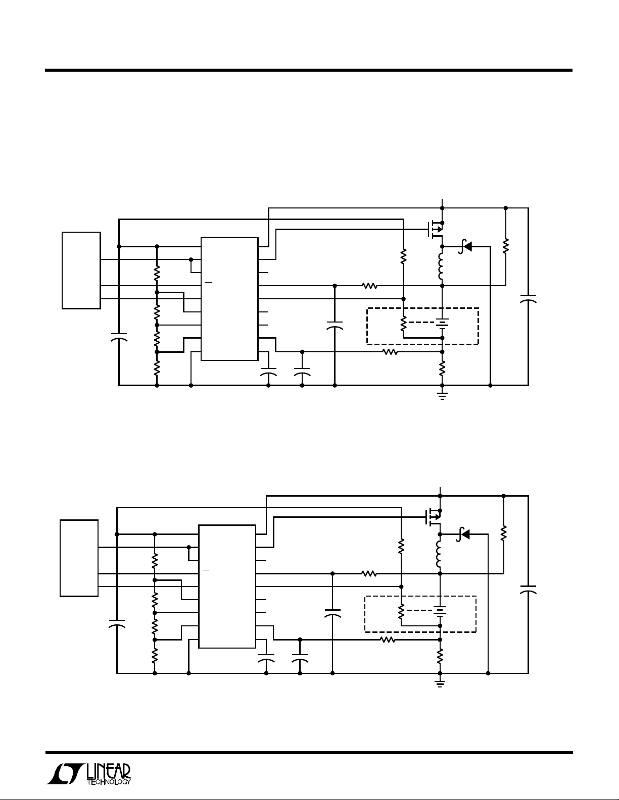
Charging “Tall” Batteries (> 8 cells)
To charge more than 8 cells, the charging supply (VDC)
must be greater than 16V (assuming 2V per cell at the end
of charge). Since VDC is above 16V, a regulator and level
shifter are required, as explained in the previous application. Figure 5 shows a circuit that will charge batteries with
more than 8 cells in series. In addition, an external battery
divider is added to limit the voltage seen at the V
BAT
pin to
below VDD. The values of R8, R9 and R10 are selected such
that R10/(R8 + R9 + R10) is the number of cells in the
battery. The battery divider in the LTC1325 is programmed
to divide by one. V
the charging current is 160mV/R
charges the 10 cell 500mA Hr stack at a C/3 rate. R
is programmed for 160mV so that
DAC
or 160mA. This
SENSE
TRK
is
selected to trickle charge the battery at C/20. The same
circuit will charge batteries at 2A if L1 and R
SENSE
are
changed to 15µH and 0.08Ω respectively.
Without R11 to R14, P2 and A1 in Figure 5, the BATP status
flag will always be high regardless of whether the battery
is present or not. It is therefore possible to start the charge
loop when the battery is not present. The current through
the charge loop will be low (typically in the milliampere
range). If this is undesirable, R11 to R14, P2 and A1 may
be added to ensure proper operation of the BATP flag. R11
and R12 are selected such that R12/(R11+R12) is the
number of cells in the battery. Op amp A1 compares the
cell voltage against a threshold set by R13 and R14. When
the battery is absent, A1 trips to turn on P2 which then
pulls V
up to VDD. This causes the BATP flag to go low
BAT
to indicate the absence of the battery.
AN64-7
Application Note 64
V
25V
DC
MPU
(e.g. 8051)
p1.4
p1.3
p1.2
C
REG
4.7µF
R7
220Ω
C2
1µF
35V
REG
D
D
CS
R1
10k
1%
+
R2
10k
1%
R3
10k
1%
NOTE 1: PANASONIC ERT-D2FHL103S NTC THERMISTORS OR EQUIVALENT.
CLK
LTF
MCV
HTF
GND
+
OUT
IN
LTC1325
D4
16V
1N4745A
VDD
PGATE
DIS
V
BAT
T
BAT
T
AMB
V
SENSE
FILTER
1µF
R4
IN
C
F
7.5k
1%
THERM 2
NOTE 1
+
R13
10k
R14
5.1k
+
Figure 5. Charging More Than 8 Cells
32V
2
500pF
+
LT1006
–
A1
P2
BS250
7
4
100Ω
6
3.3µF
+
+
D3
10V
1N4740A
C2
0.1µF
35V
R5
7.5k
1%
THERM 1
NOTE 1
R16
100k
COILTRONICS
CTX100-1-52
100µH
100Ω
P1
IRF9531
D2
1N5818
L1
D1
1N5818
V
BAT
10 CELLS
500mA HR
C/3 RATE
R
SENSE
1Ω
C/20 TRICKLE
R8
11.3k
1%
R9
78.7k
1%
R10
10k
1%
R
TRK
200Ω
1/4W
R11
91k
R12
10k
C
SPLY
10µF
AN64 F05
+
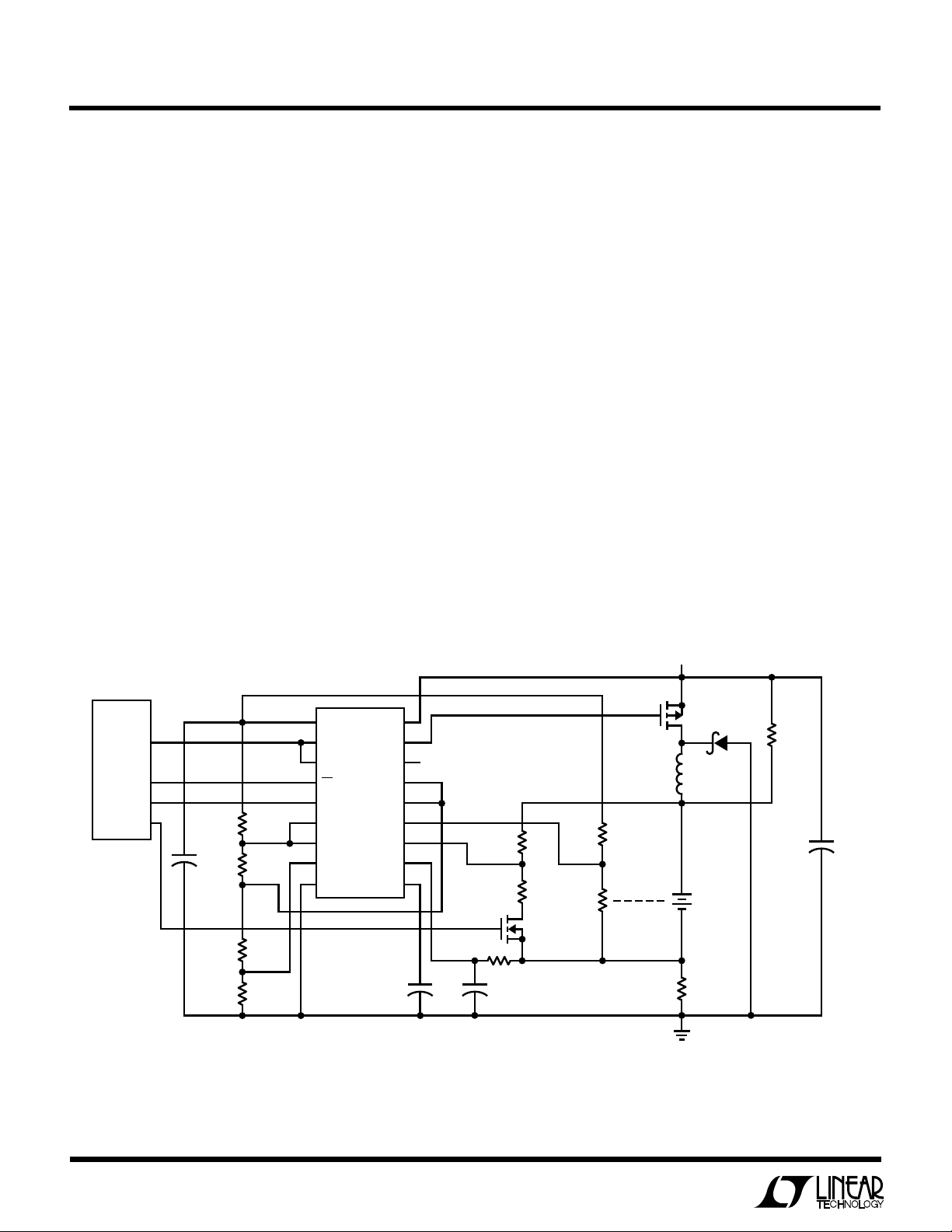
Hardwired Charge Termination Using Thermistors
Termination Using Positive Temperature Coefficient
(PTC) Thermistors: The resistance of a PTC thermistor
increases sharply when its temperature rises above a
specified setpoint (TS). This rapid change may be exploited to implement hardwired TCO charge termination.
In Figure 6, fixed resistor R4 is connected from REG to the
T
input, and the PTC thermistor R5 is connected
BAT
between the T
input and Sense. Hence R5 is the
BAT
controlling element of a temperature-dependent voltage
divider. The PTC is mounted on the battery to sense its
temperature. R4 is selected such that when the battery
temperature is below TS, the divider output voltage is
between the voltages at the LTF and HTF pins. When the
battery temperature rises above TS, the rapid increase in
the resistance of the PTC device causes the divider output
(i.e. the voltage at the T
pin) to rise above the voltage
BAT
set by R1, R2 and R3 at the LTF pin. The LTC1325 detects
a temperature fail-safe (LTF = 1, FS = 1) and stops charging
by taking the PGATE pin to VDD. A typical value for TCO is
45°C. TS and R
THERM1
have typical tolerances of ±5°C and
±40% respectively. The PTC shown in Figure 6 has a TS of
50°C ±5°C, so charging will terminate when the battery
temperature reaches a value between 45°C and 55°C. The
series resistance of PTC thermistor and R4 should be in
the kΩ range to minimize loading on the REG pin of the
LTC1325.
In principle, it is possible to implement hardwired ∆TCO
termination by replacing R4 with another PTC with a
resistance vs temperature characteristic that matches that
of R5 as shown in Figure 7. If both PTCs match closely, the
divider output will now respond to the difference between
AN64-8
Application Note 64
battery and ambient temperature. In practice, matched
PTCs are not generally available as standard items from
thermistor manufacturers and are therefore not recommended for such use. If hardware ∆TCO termination is
desired, standard NTCs such as those matched over a
MPU
(e.g. 8051)
p1.4
p1.3
p1.2
REG
D
OUT
R1
R2
+
C
REG
4.7µF
R3
R4
D
IN
CS
CLK
LTF
MCV
HTF
GND
LTC1325
VDD
PGATE
DIS
V
BAT
T
BAT
T
AMB
V
SENSE
FILTER
IN
+ +
C
1µF
F
specified temperature range may be used. With NTCs, the
divider output will drop as the battery heats up and when
the voltage drops below the voltage at the HTF pin, the
LTC1325 will detect a temperature fail-safe (HTF = 1,
FS = 1) and terminate charging.
V
DC
16V MAX
P1
D1
R
TRK
AN64 F06
+
C
SPLY
10µF
500pF
R4
100Ω
+
3.3µF
PTC
THERM 1
100Ω
L1
V
8 CELLS
MAX
R
SENSE
BAT
MPU
(e.g. 8051)
p1.4
p1.3
p1.2
Figure 6. Hardwired TCO Termination
V
DC
12V
P1
D1
R
TRK
AN64 F07
+
C
SPLY
10µF
LTC1325
VDD
PGATE
DIS
V
BAT
T
BAT
T
AMB
V
SENSE
FILTER
IN
+ +
C
1µF
THERM 1
100Ω
+
F
500pF
3.3µF
THERM 2
100Ω
L1
V
BAT
8 CELLS
MAX
R
SENSE
REG
D
OUT
R1
R2
+
C
REG
4.7µF
R3
R4
D
IN
CS
CLK
LTF
MCV
HTF
GND
Figure 7. Hardwired ∆TCO Termination
AN64-9
Application Note 64
Termination Using Negative Temperature Coefficient
(NTC) Thermistor: It is common for the thermistor in the
battery pack to be terminated at the negative terminal of
the battery. During charging, the Sense pin will exhibit a
switching waveform with peaks of 200mV to 300mV when
V
is programmed for 160mV. This waveform appears
DAC
on the T
pin when the thermistor is terminated at the
BAT
negative terminal of the battery. The thermistor slope is
typically –30mV/°C, so the switching noise can cause
premature fail-safes when the battery temperature is within
10°C of the LTF or HTF trip points. An RC filter (with time
constant much greater than the clock period of 10µ s) can
be inserted between the T
pin and the output of the
BAT
battery thermistor circuit to prevent false fail-safes.
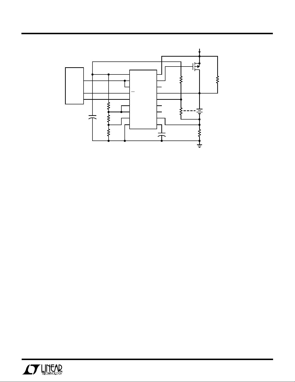
Disabling Fail-Safes
The LTC1325’s built-in battery voltage and temperature
fail-safes can be easily disabled as shown in Figure 8. To
disable temperature fail-safes, the T
pin is tied to the
BAT
top of resistor R3. The LTC1325 is made to think that the
battery temperature is constant and within the limits set by
the LTF and HTF pins. Similarly, V
may be tied to the
BAT
same point to disable all the battery voltage fail-safes
(MCV, EDV, BATR). The LTC1325 battery divider is programmed to divide-by-1. Battery temperature and cell
voltage can still be measured using the T
AMB
and V
IN
channels of the ADC. An external divider (R7, R8) replaces
the internal divider connected to the V
channel.
BAT
Gated P-Channel MOSFET Controller
When an external current-limited voltage source is available, and charging currents are low enough that efficiency
and heat dissipation are not major concerns, the LTC1325
can be used to turn on a P-channel MOSFET to gate the
current into the battery. This circuit makes an inexpensive
and effective combination. The battery’s current limit
during charging is set by the current limit of the charging
power supply VDC . The maximum available current should
therefore not exceed the permissible charge rate of the
battery. With the LTC1325 V
programmed to the
DAC
160mV setting, and the voltage at the Sense pin below this
value, the LTC1325 will hold MOSFET P1 on until charge
MPU
(e.g. 8051)
p1.4
p1.3
p1.2
p1.5
LTC1325
VDD
PGATE
DIS
V
BAT
T
BAT
T
AMB
V
SENSE
FILTER
IN
+ +
C
1µF
F
REG
D
OUT
D
IN
CS
R1
10k
REG
1%
R2
4.99k
1%
R3
4.99k
1%
R4
10k
1%
+
C
4.7µF
25V
NOTE 1: PANASONIC ERT-D2FHL103S NTC THERMISTOR OR EQUIVALENT.
NOTE 2: CHOOSE FOR C/20 TRICKLE CHARGE RATE.
CLK
LTF
MCV
HTF
GND
100Ω
500pF
R7
30.1k
1%
R8
10k
1%
Q1
VN2222LL
100µH
COILTRONICS
CTX100-1-52
R9
7.5k
1%
THERM 1
NOTE 1
V
DC
16V MAX
L1
R
1Ω
P1
IRF9531
D1
1N5818
V
BAT
500mA HR
SENSE
R
TRK
NOTE 2
AN64 F08
+
C
SPLY
10µF
AN64-10
Figure 8. Charger with T
BAT
and V
Fail-Safes Disabled
BAT
MPU
(e.g. 8051)
p1.4
p1.3
p1.2
LTC1325
VDD
PGATE
DIS
V
BAT
T
BAT
T
AMB
V
SENSE
FILTER
R4
7.5k
1%
IN
+
NTC
THERM 1
NOTE 1
C
F
1µF
REG
D
OUT
D
IN
CS
R1
10k
C
REG
4.7µF
1%
R2
10k
1%
R3
10k
1%
+
NOTE 1: PANASONIC ERT-D2FHL103S NTC THERMISTOR OR EQUIVALENT.
NOTE 2: CHOOSE FOR C/20 TRICKLE CHARGE.
CLK
LTF
MCV
HTF
GND
Application Note 64
V
DC
16V MAX
P1
IRF9531
R
TRK
NOTE 2
V
BAT
4 CELLS
500mA HR
R
SENSE
1Ω
AN64 F09
Figure 9. LTC1325 Charger Using an External Constant-Current Supply
is terminated by the microprocessor, or a fail-safe occurs.
As shown in Figure 9, the inductor and catch diode that are
normally connected to the positive terminal of the battery
are not required, as no PWM switching action occurs at the
drain of MOSFET P1.
With the wall adapter connected, the current into the
battery will always be (I
ADAPTER
– I
EQUIPMENT
). The use of
one additional operational amplifier, such as the LT1077,
allows monitoring this charging current by integrating the
voltage across R
during the charging interval. The
SENSE
result of this integration can then be measured using the
LTC1325’s auxiliary ADC input VIN. Combined with the
built-in gas gauge function during the discharge interval
(via the Sense input), the state of charge of the battery may
be reliably determined at any time.
If the battery pack is heavily depleted or is damaged, the
wall adapter can still be used to operate the equipment by
putting the LTC1325 into Idle mode. Under these conditions the battery will receive no charging current (except
through the trickle charging resistor, if one is provided). If
the gas gauge is not needed, R
can be removed and
SENSE
the Sense pin should be returned to ground.
Constant-Potential Charging (Lead-Acid and
Lithium-Ion)
Constant-current charging, which is the technique of
choice for NiCd and NiMH batteries, is not recommended
for most Lead-Acid or Lithium-Ion applications. Instead, a
constant-voltage charging regimen is required, usually
with a means of limiting the initial charging current. Such
a charging technique is generally referred to as a “Constant-Potential” (CP) regimen.
The LTC1325 is at first glance a constant-current part.
Such a view of its capabilities, however, is too limited. Its
power control section is more completely described as a
constant-average-current PWM with both hardware and
software feedback. The hardware loop used for current
sensing is the Sense input; the software loop, which can
be used to control the effective output voltage of an
LTC1325 charger circuit, is the microprocessor control
routine in conjunction with the ADC and the DAC. Given a
suitable output filter (the output inductor and the battery
itself), current from the PWM section can be made to
produce a current-limited constant voltage at the battery’s
terminals. A circuit intended for such CP operation is
shown in Figure 10.
AN64-11

Application Note 64
MPU
(e.g.,80C51)
+
C
4.7µF
NOTE 1: PANASONIC TYPE ERT-D2FHL103S NTC THERMISTOR OR EQUIVALENT
REG
R
R
P1.4
P1.3
P1.2
P1.5
MCV1
MCV2
4
DATA
3
CHIP SELECT
2
CLOCK
5
AUX SHDN
1
REG
2
D
OUT
3
LTC1325
D
R
TF1
R
TF2
R
TF3
IN
4
CS
5
CLK
6
LTF
7
MCV
8
HTF
9
GND
VDD
PGATE
DIS
V
BAT
T
BAT
T
AMB
V
SENSE
FILTER
IN
1µF
18
17
16
15
14
13
12
11
10
CF
Figure 10. Constant Potential Battery Management System
+
R1
7.5k
1%
THERM 2
NOTE 1
+ +
C
S
500pF
R5
470k
R3
R4
Q1
2N7002
RIN
2k
R
100Ω
CIN
47µF
VDC IN
P1
IRF9Z30
R
R2
7.5k
1%
THERM 1
NOTE 1
S
R
SENSE
62µH
L1
Y
TRK
D1
1N5818
R
DIS
IRF510
+
N1
AN64 F10
C
SPLY
10µF
Batteries that require a CP charging algorithm generally
need a rather accurate charging voltage, especially in fastcharge applications. For this reason the LTC1325’s internal battery divider often cannot be used to control the
charging voltage, due to its tolerance of ±2% at division
ratios other than 1:1. It does, however, remain useful for
MCV and/or FEDV detection. For measuring battery voltage an external resistive divider feeding VIN is recommended. The external divider resistors should be chosen
such that the voltage at the VIN pin will come as close as
possible to the ADC’c full-scale input voltage without
exceeding that value; 3.000V maximum is a good choice.
Using a near-full-scale input to the ADC improves measurement accuracy. To further improve charging voltage
accuracy, it’s a good idea to use ±0.1% or ±0.25%
tolerance resistors in the battery voltage divider. Under
such conditions, the voltage loop error is ideally only the
reference error (±0.8%), plus that of the ADC (4 bits out
of 1024, or ±0.4%) and of the battery divider (±0.1% or
±0.25%), for a total ±1.3% or ±1.5% error.
“Auxiliary Shutdown” is a static line from the microprocessor to a small-signal MOSFET, which prevents the
battery from discharging through the voltage divider string
when it is not charging. With the external divider in place,
the BATP flag will always be high except when Auxiliary
Shutdown is at a logic low and the battery is not installed
in the circuit (see “Charging ‘Tall’ Batteries” above). Battery voltage fail-safes will remain operational (assuming
that they use the V
input) although it may not be
BAT
possible to make simultaneous use of the MCV and EDV
fail-safes with all CP battery types. R
, if needed, main-
TRK
tains the battery in a fully charged condition.
A suitable software algorithm to implement a quasi-CP
charger is this:
1. Establish a regular repetition interval for the voltage
servo loop. t
values of 10ms to 20ms give good
LOOP
results.
2. Set V
to 160mV at the highest charge rates for best
DAC
resolution. Using a 95% maximum PWM duty cycle
[tON/(tON + t
I
), where I
MAX
)], R
OFF
is the nominal maximum current to
MAX
chosen as 160mV/(0.95 ×
SENSE
be allowed through the battery. A suitable minimum
duty cycle is 10%; beyond such a low duty cycle it is
AN64-12

Application Note 64
usually better to reduce the peak current through the
battery (by programming V
) than to reduce the duty
DAC
cycle further.
3. Perform each of the following tasks once each servo
loop interval (t
LOOP
):
a) Enter Idle mode of operation.
b) Read V
CELL
.
c) Adjust the value entered into a timer register (or
a software timer) up or down according to actual
V
vs target V
CELL
value is increased. If V
CELL
. If V
is too low, the timer
CELL
is too high, the timer
CELL
value is decreased.
d) The maximum Charge time of the LTC1325 has
been set at 95% of t
; the minimum at 10%.
LOOP
Within that range, the duty cycle at which the loop
will operate is set by the timer of 3(c). If the timer’s
interval is increased (V
each t
during which the LTC1325 is put into
LOOP
too low), the portion of
CELL
Charge mode is increased. If the timer’s interval is
decreased (V
is too high), the LTC1325 is com-
CELL
manded into Idle mode for a greater portion of each
t
.
LOOP
e) If tON < (0.1 × t
value (note that the V
), switch V
LOOP
to the next lower
DAC
value of 34mV is not used).
DAC
f) Repeat (a) through (e) until the average current into
the battery, or the net duty cycle, drops below a
chosen limit. A timer-based secondary cutoff is
often recommended for CP chargers.
g) Terminate the software loop with MOSFET P1 in the
“off” state, using R
(if required) to maintain the
TRK
battery’s charge.
A flow chart showing the principals of this voltage servo
loop is given in Appendix B, Figures B3a and B3b. Figure
B3a shows the “ramp-up” from the point where the
charger is first turned on to the maximum charging
current required and Figure B3b shows the “taper-down”
which simulates the necessary CP charging algorithm.
(This algorithm is undergoing refinement at press time.
For the latest information on its implementation and
optimization, please contact LTC.)
RIN and CIN have greater values in Figure 10 than in most
of the circuits in this Application Note. This is because
batteries requiring a CP charge tend to have a significant
positive ∆V during the interval in which charging current
is flowing through them. The time constant of (RIN × CIN)
filters the resulting 10ms to 20ms ripple before it is
presented to the V
and VIN pins. If only VIN input will be
BAT
used, RIN may be omitted, CIN may be placed from VIN to
ground, and its value can be decreased.
The circuit of Figure 10 has deliberately been generalized
to provide flexibility across all common battery types. For
applications requiring the support of only specific battery
types, or which do not need extensive thermal or other
protection mechanisms, various components can be
modified or removed to minimize cost and board space.
Overcurrent Protection
Three common scenarios in which battery current can
exceed acceptable levels are: accidental shorting of the
battery terminals, excessive loads and inserting the battery into the charger in reverse. Battery or charger damage
in all three cases can be prevented through the use of a
thermal or overcurrent device to limit fault currents.
Usually, it is desirable that this device reset itself when the
fault goes away. Possible choices are bimetallic (thermostatic) switches and polymer PTC thermistors. The high
series resistance of traditional ceramic PTC thermistors,
even in the unexcited state, make them unsuitable for this
application.
Bimetallic switches operate by sensing battery temperature. By the nature of their operation, these switches cycle
on and off as long as the fault remains, causing the battery
and all associated components (mechanical as well as
electrical) to heat up and cool down repeatedly. Polymer
based PTC thermistors such as the Raychem PolySwitch
®
also offer very low series resistance until “tripped,” and
have the advantages of a faster response and freedom
from thermal cycling.
Polymer PTCs should be chosen such that under normal
operation, the average charging current (V
DAC/RSENSE
) is
less than the Hold Current rating of the PTC to keep it in the
low resistance state. Under fault conditions, the Fuse
Current should exceed the Trip Current rating of the fuse.
This will cause the fuse’s resistance to increase dramatically and reduce the fault current to about V
PolySwitch is a registered trademark of Raychem Corporation.
BAT/RFUSE
(Trip).
AN64-13
Application Note 64
The PolySwitch should ideally be placed between cells in
the battery, in close physical contact with one of the cells.
In this way the trip point of the device will be reduced as
the battery’s temperature increases. Such a configuration
provides substantial protection for the battery against
shorts across its terminals and from excessive load currents. It will also protect the battery if it is accidentally
inserted into the charger in reverse.
Figure 11 shows the fault current path when a battery is
inserted into a charger in reverse. Potentially damaging
currents may flow through this path since the Sense
resistor is usually in the region of 1Ω or less. A PolySwitch
inside the battery pack (as described above), or in series
with the Schottky diode, limits fault currents to safe levels.
The following points should be noted in choosing the
diode and R
SENSE
.
• Normal charging currents should be equal to or less
than the holding current rating of the PolySwitch.
• Temperature affects PolySwitch performance. The
manufacturer’s data should be consulted for derating
factors.
• Initial fault currents will be approximately V
BAT/RSENSE
if the battery is inserted in reverse. This should exceed
the trip current rating of the PolySwitch.
• The surge current rating of D1 should exceed the initial
fault current of V
BAT/RSENSE
. It may be necessary to
confirm the selected diode’s applicability with the manufacturer of the part.
In addition to the above scenarios, the battery current may
exceed acceptable levels when a battery is inserted into a
charger which has the charging supply (VDC) turned off. If
the VDC supply exhibits a low impedance path to ground
when it is turned off, the diode that is intrinsic to the
P-channel MOSFET may turn on to form a battery discharge path which flows from the battery’s positive terminal through the inductor, the MOSFET internal diode, the
ground lead and the sense resistor before returning to the
negative terminal of the battery. This can be prevented by
connecting a Schottky diode between VDC (diode anode)
and the source of the P-channel. See the section on
“Current Sinking VDC Sources” for more details.
Current-Sinking VDC Sources
In some applications, it may be necessary to add a
Schottky rectifier between the VDC supply and the source
of MOSFET P1. This rectifier prevents the battery from
discharging backwards through MOSFET P1, which could
damage P1, L1, or R
. It is required if the following
SENSE
conditions are met:
• The wattage of R
should be high enough to
SENSE
withstand the initial fault currents of V
MPU
(e.g., 8051)
p1.4
p1.3
p1.2
C
REG
4.7µF
R1
R2
R3
+
REG
D
D
CS
CLK
LTF
MCV
HTF
GND
.
R4
+
CF
1µF
THERM 2
+
+
500pF
OUT
IN
LTC1325
BAT/RSENSE
VDD
PGATE
DIS
V
BAT
T
BAT
T
AMB
V
IN
SENSE
FILTER
Figure 11. Reversed Battery Protection
3.3µF
IRF9531
R5
100Ω
THERM 1
100Ω
V
DC
12V
P1
D1
R
TRK
L1
+
R
SENSE
FUSE
AN64 F11
C
SPLY
10µF
AN64-14

Application Note 64
• The voltage of the battery being charged can exceed
that of the supply.
• The VDC supply can sink current when it is at a lower
voltage than the battery being charged.
Most switching power supplies, such as those used for AC
adapter and battery charger supplies in portable computers, have a very small reverse leakage current––several
milliamperes at most. These would not generally need the
additional Schottky rectifier. Two examples of situations
where the rectifier is necessary are:
• Charging a 7.2V or greater battery from a 12V car
battery using the cigarette lighter socket. Under coldcranking conditions the 12V nominal battery drops to
6V to 7V and an automobile’s wiring will allow the
starter motor to pull current back out of the lighter
socket.
• Bench-top testing. Many power supplies have internal
protection circuitry which will sink current from the
load rather than allow a sourcing load, such as a
charged battery, to force current indiscriminately into
the supply’s output. Also, any supply with a crowbar
represents a possible current-sinking power supply.
Figure 12 depicts a basic charger circuit and shows the
proper placement of the Schottky rectifier DIN.
CONCLUSION
Through its ability to accept commands from almost any
microprocessor, the LTC1325 takes advantage of the
power and flexibility of software to avoid locking the user
into any given battery type. This almost endless
configurability enables the battery system designer to
choose the required charge regimen, charge rate and
charge termination technique(s) for virtually any task.
Possibilities range from a robust but basic battery charging technique to sophisticated multiple-stage charging
algorithms, or even several different algorithms entirely,
all executed with the same hardware. In this way a wide
range of battery types or end application needs can be
accommodated with the same circuit. The on-board fault
detection circuitry provides additional confidence in the
final design by acting as a “watchdog” on the microprocessor and the battery pack. The design of the overall
charging circuit is made as simple as possible by incorporating all the functional blocks needed and minimizing the
discrete component count. In addition to charging batteries, the LTC1325 has provisions to condition batteries and
to measure battery capacity. As with the LTC1325’s charging-related functions, these capabilities are afforded a
maximum of versatility and value by being placed almost
completely under software control.
MPU
(e.g., 8051)
p1.4
p1.3
p1.2
V
DC
D
(20V SCHOTTKY)
IN
P1
IRF9531
LTC1325
VDD
PGATE
DIS
V
BAT
T
BAT
T
AMB
V
SENSE
FILTER
IN
+ +
C
1µF
F
R5
THERM 2
500pF
R6
100Ω
+
THERM 1
3.3µF
100Ω
DC
REG
D
OUT
R1
C
REG
4.7µF
R2
R3
R4
+
D
IN
CS
CLK
LTF
MCV
HTF
GND
Figure 12. Protection Against Discharging Through V
L1
R
D1
SENSE
FUSE
R
TRK
AN64 F012
+
C
SPLY
10µF
AN64-15

Application Note 64
APPENDIX A
An Overview of Battery Types, Terminology, and
Techniques
The world is increasingly relying upon portable electronic
equipment, and the rechargeable battery systems (battery, battery charger and ancillary functional blocks)
which power that equipment. These battery systems are
among the defining elements of end product capability,
endurance and life. In spite of this, they are commonly
considered a necessary evil; their design and testing, a
black art. The truth is that commercially viable battery
management systems are comprised of well understood
electronic and electrochemical components, with well
defined performance characteristics. While this Appendix
is not intended as a comprehensive treatment of battery
technology, it will provide the equipment engineer with
practical information for the choice of battery types and
battery management techniques.
There are three rechargeable battery types commonly
used in portable devices. These are Nickel-Cadmium (NiCd),
Nickel-Metal Hydride (NiMH) and Sealed Lead-Acid (SLA).
Lithium-Ion (Li-Ion) is also beginning to receive significant attention, primarily due to its very high energy density
(as measured in terms of volume and of weight). Table A1
gives a quick overview of the characteristics of these
battery types:
Table A1. Battery Type Characteristics
BATTERY SEALED LITHIUMCHARACTERISTICS LEAD-ACID NiCd NiMH ION
Energy Density 30 40 60 90
W-h/kg
Energy Density 60 100 140 210
W-h/liter
Cell Voltage (V) 2.0 1.2 1.2 4.20 Max
3.60 Avg
2.50 Min
Charging Method Constant Constant Constant Constant
Potential Current Current Potential
Dicharge Profile Mildly Flat Flat Sloping
Sloping
#Charge/Discharge 300 >500 >500 500 to
Cycles* 1000
Self-Discharge 3%/MO 15%/MO 20%/MO 6%/MO
Internal Resistance Low Lowest Moderate Highest
Discharge Rate** > 4C > 10C 3C < 2C
* Until 80% of rated capacity is available upon discharge.
** C is the capacity rating of the battery in Ampere-Hours.
A useful first-approximation view of a rechargeable battery is that it is a container into which energy may be
poured as desired, to be subsequently consumed as
needed. This analogy generally conjures up an image of a
jar of water, which would impose few restrictions upon
rates of filling or emptying the vessel. In fact, a battery is
more akin to a bottle of thick syrup, with the bottle having
a narrow mouth and a wide base. With such a bottle, the
syrup must be delivered into the bottle at a controlled rate
and pressure (to prevent possible damage to the delivery
system or to the neck of the bottle), and may be drawn at
a maximum rate determined by the amount of syrup in the
bottle and the bottle’s shape. To carry this analogy just a
little further, it is true of batteries, as it is with the
hypothetical syrup bottle, that it is possible to get almost
all of the contents out of the container — but it may take
a long time to get the last few percent out. The flow rate will
vary with the amount remaining, meaning that in situations where a high rate of discharge is required of a
battery, not all the “contents of the bottle” — not all the
available energy — will be instantaneously available to the
discharging circuit.
Battery recharge times generally break down into several
groups. The most common of these are the “standardcharge,” suitable for overnight applications (typically requiring 16 hours) and the “fast-charge” (typically two
hours or less). Between the two is the “quick-charge,”
which is in many respects akin to a standard-charge but
requires a useably shorter interval (about five hours).
Examples of standard-charge applications are cordless
telephones and UPS systems for small computers. Quickcharge batteries are commonly found in devices which will
see brief but significant power drain several times daily,
such as cellular phones. Laptop computers and cordless
tools are excellent locations for fast-charge systems. In
these and other fast-charge uses there is a high average
drain on the battery, and the product’s value is determined
in large part by the availability of battery power upon
demand. The LTC1325 forms a comprehensive core for
battery management systems operating at any of these
charge rates; all that need be changed are a few external
components and the microprocessor algorithm used to
control the charge cycle. Only batteries designed and
rated for fast-charge should be subjected to a fast-
AN64-16

Application Note 64
charge regimen. Similarly, only batteries rated for quickcharge should be subjected to quick-charging conditions.
As might be expected, there are important differences
between the charging regimens used for the four different
battery types. There are also more similarities than might
be expected. Each of the following sections is intended to
stand alone, but it is suggested that the battery system
designer read all four sections in order to get a feel for
where the similarities and differences between battery
families lie. Terms which are specific to the battery user
community, or which have special meanings in this Appendix, are defined in the Glossary in Appendix C.
Using Nickel-Cadmium Batteries
Nickel-Cadmium batteries, in various forms, have been in
use for over 50 years. During that time they have evolved
from expensive, special purpose devices to the battery of
choice for most portable equipment. The availability of
inexpensive sealed cells, with ongoing improvements in
energy density and cycle life, have been the driving forces
for this acceptance. The LTC1325 adds to this the ability to
easily implement fast-charge routines, gas gauge algorithms and/or switch mode constant current sources, all
using very little system overhead and printed circuit board
space.
• Special purpose batteries are available with extended
operating temperature ranges.
The “cons”:
• Cadmium is commonly considered an environmentally
hazardous material. Nickel is also coming under environmental scrutiny.
• NiCd cells have a significant self-discharge rate (0.5%/
day at room temperature).
Nickel-Cadmium Standard-Charge
For applications which can allow a recharge period of
about 16 hours — an “overnight” charge — the standardcharge regimen is the method of choice. The reasons for
this include:
• Simplest charging algorithm.
• Least expensive charge termination techniques.
• Small power supply required to provide the charging
current.
• Small charging circuit power components.
• Low overall charging system power dissipation.
A standard-charge is relatively straightforward to implement. In “cookbook” form, such a charge requires:
A quick run-down of the pros and cons of Nickel-Cadmium
batteries:
The “pros”:
• Good energy density, both by weight and by volume,
relative to competing technologies.
• Acceptable charging rates range from 0.1C to 2C and
beyond.
• Most NiCd cells can accept a continuous overcharge
current of 0.1C.
• A very flat discharge profile.
• The lowest cell impedance of the major battery technologies.
• Well understood and documented electrical behavior
and electrochemistry.
• Cells and batteries are available in a variety of sizes
from a number of vendors.
• Charging Current: 0.1C.
• Required Charging Voltage: 1.60V/cell or greater, plus
charger overhead.
• Charging Temperature Range: 0°C to 45°C.
• Charging Time: 16 hours.
• Charge Termination Method: None required.
• Secondary Charge Termination Methods: None required.
• Special issues which may require further consideration
are: wide temperature range charging, wide temperature range discharging and accurate gas gauging at
temperature extremes.
A charging current of 0.1C, fed to the battery for 16 hours,
will deliver (16 hours × 0.1C) = 160% of standard capacity
to the battery. At temperatures between 0°C and 25°C, the
resulting 60% overcharge is adequate to ensure that the
battery is returned to 100% of its standard capacity. Once
AN64-17

Application Note 64
the cells in the battery reach their actual capacity for the
operating temperature, mild gassing will occur, but not
enough to cause venting or other cell damage. Since most
NiCd batteries will accept a continuous 0.1C charge at any
case temperature between 0°C and 50°C, charge termination per se is usually not required. For specialized applications, extended temperature range batteries are available
which can be charged at 70°C. Charging at temperatures
below 0°C is also possible if the charge current is “throttled
back” as the battery temperature decreases. The charging
current under such conditions should linearly decrease
from 0.1C at 0°C to zero current at –15°C to –25°C. In
wide temperature range applications, the use of a battery
(or ambient) temperature sensor in conjunction with the
LTC1325 is an excellent way to provide positive control of
battery charging current versus temperature, thereby extending battery life.
The charge acceptance of NiCd batteries is reduced significantly at temperatures above 40°C. This effect is only
marginally mitigated by longer charge times, and should
be taken into account if gas gauging is to be done over
extended temperature ranges. By way of example, a battery that can be fully recharged at 25°C in 16 hours will
reach only about 75% of standard capacity at 45°C after 48
hours. Again, no damage will be done to the battery, but its
available capacity during subsequent discharge will be
less than one would otherwise expect. If correction parameters for the gas gauging function of the LTC1325
will be employed, it is recommended that the manufacturer of the specific battery in question be consulted.
In the same way that charge acceptance is reduced for
temperatures above 25°C, actual capacity is reduced
when discharging a cell at temperatures much removed
from 25°C. The battery temperatures at which actual
capacity is 85% of standard capacity are approximately
0°C and 50°C. Again, for more specific data, the manufacturer of the battery to be used should be contacted.
the charger’s output current to a 0.05C trickle-charge after
the five-hour recharge interval. Checking the cell
manufacturer’s data will provide further information on
this, as well as the specified charge rate, permissible
continuous overcharge rate, and information on the allowable temperature range.
Under some conditions, it may be desirable to use a lower
charging rate than 0.1C (for instance, to reduce charger
power requirements). This is feasible only within a narrow
range: NiCd cells have a reduced charge acceptance at
lower charge rates, lengthening the required charge time.
This, and their self-discharge characteristic (approximately
0.5%/day at 23°C), combine to make anything under
0.05C a very slow and potentially unreliable charge rate for
most cell types.
Nickel-Cadmium Fast-Charge
In recent years a class of applications has arisen for which
5 hours to 16 hours may constitute an excessive recharge
time. Portable computer equipment is an excellent example of this — even if the battery pack in a laptop can be
“swapped out” for external recharge, it is often needed
again within several hours, fully charged and ready for
use. In this case, the fast-charge techniques which the
LTC1325 makes practical are the way to go. A fast-charge
regimen implies:
• 90% recharge within one hour; 100% recharge within
two to three hours.
• A method for determining the optimum charge termination point(s).
• Backup charge termination method(s) to ensure best
battery life.
• Highly efficient use of available charging energy.
• Increased product value through better battery utilization and greater customer satisfaction.
Specially rated NiCd cells can support a higher rate of
relatively uncontrolled overcharge than the ubiquitous
0.1C. This allows the quick-charge regimen, which is
typically 0.33C for 5 hours. Charging current and interval
aside, most other details for performing a quick-charge
are the same as for a standard-charge. It is often desirable
in quick-charge regimens to use a timed charge, reducing
AN64-18
Unlike the standard-charge and quick-charge regimens,
there is no one best way to fast-charge a Nickel-Cadmium
battery. Variables introduced by the allowable cost and
size of the end application, the continuing evolution of
Ni-Cd cells to accomodate faster charge rates, and the
specific battery vendor(s) chosen will all influence the final
choice of charging technique. There are several areas of

Application Note 64
industry consensus, however, regarding the suitable fastcharging of NiCd batteries:
• Charging Current: 1.0C to 2.0C.
• Required Charging Voltage: 1.80V/cell or greater, plus
charger overhead.
• Charging Temperature Range: 10°C to 40°C.
• Charging Time: Three hours (90% of charge is typically
returned within the first hour).
• Suitable Charge Termination Methods: See Table A2.
• Suitable Secondary Charge Termination Methods: See
Table A2.
• Special issues which may require further consideration
are: accurate gas gauging at temperatures over 25° C,
and appropriate mechanical integration of the battery
pack into the end equipment.
The objective of fast-charging a NiCd battery is, crudely
stated, to cram as much energy as it takes to bring the
battery back to a fully charged state into that battery in as
short a time as possible. Since current is proportional to
energy divided by time, the charging current should be as
high as the battery system will reasonably allow. Generally, NiCd batteries rated for fast-charge use are designed
around a 1C to 2C maximum charging rate. At the 1C rate,
more than 90% of the usable discharge capacity of the
battery is typically returned within the first hour. Higher
rate cells (up to 5C) do exist, but they are more oriented to
special applications and will not be discussed here, except
to note that the LTC1325 is capable of handling the
charging routines required for such cells, should that be
required.
Fast-charging has compelling benefits, but places certain
demands upon the battery system. A properly performed
fast-charge can yield a cell life of as many as 500 charge/
discharge cycles. The high charging rates involved, however, do engender correspondingly more rapid electrochemical reactions within the cell. Once the cell goes into
overcharge, these reactions cause a rapid increase in
internal cell pressure, and in the cell’s temperature. Figure
A1 shows the Voltage, Pressure and Temperature characteristics of a Nickel-Cadmium cell being charged at the 1C
rate. It can be seen that, as the cell approaches 100% of
Table A2. Fast-Charge Termination Techniques for Nickel-Cadmium Batteries
Voltage Cutoff (VCO) Uses absolute cell voltage to determine the cell’s state of charge. Not generally recommended for use
in NiCd charging regimens.
Negative ∆V (–∆V) Looks for the relatively pronounced downward slope in cell voltage which a NiCd exhibits (≈30mV to
50mV) upon entering overcharge. Very common in NiCd applications due to its simplicity and reliability.
Zero ∆V Waits for the time when the voltage of cell under charge stops rising, and is “at the top of the curve”
prior to the downslope seen in overcharge. Sometimes preferred over –∆V, as it causes less
overcharging.
Voltage Slope (dV/dt) Looks for an increasing slope in cell voltage (positive dV/dt) which occurs somewhat before the cell
reaches 100% returned charge (prior to the Zero ∆V point). No longer widely used.
Inflection Point Cutoff (d2V/dt2, IPCO) As a NiCd cell approaches full charge, the rate of its voltage rise begins to level off. This method looks
for a zero or, more commonly, slightly negative value of the second derivative of cell voltage with
respect to time.
Absolute Temperature Cutoff (TCO) Uses the cell’s case temperature (which will undergo a rapid rise as the cell enters high-rate overcharge)
to determine when to terminate high-rate charging. A good backup method, but too susceptible to
variations in ambient temperature conditions to make a good primary cutoff technique.
Incremental Temperature Cutoff (∆TCO) Uses a specified increase of a NiCd cell’s case temperature, relative to the ambient temperature, to
determine when to terminate high-rate charging. A popular, relatively inexpensive and reliable cutoff
method.
Delta Temperature/Delta Time (∆T/∆t) Uses the rate of increase of a NiCd cell’s case temperature to determine the point at which to terminate
the high-rate charge. This technique is inexpensive and relatively reliable as long as the cell and its
housing have been properly characterized.
AN64-19

Application Note 64
1.75
1.50
1.25
1.00
0.75
CELL VOLTAGE (V)
0.50
0.25
0
Reproduced with permission by Butterworth-Heinemann,
Batteries Applications Handbook
Figure A1. NiCd Voltage, Pressure, and Temperature
Characteristics During Charge at 1C (23°C Ambient)
120
100
80
60
40
20
INTERNAL PRESSURE (PSIG)
0
–20
90
80
70
60
50
40
CELL TEMPERATURE (°C)
30
20
0
, copyright 1992
CHARGE INPUT (% OF CAPACITY)
CELL VOLTAGE
PRESSURE
50 100
TEMPERATURE
Rechargeable
150
AN64 FA01
capacity, the charging current must be reduced or terminated. Left unchecked, overcharge at the C rate will ultimately cause the cell’s safety vent to open. This results in
a loss of gaseous electrolyte to the ambient, and a permanent diminution of cell capacity. Similarly, allowing the
temperature of the cell to rise excessively will cause a
degradation of the internal materials, again reducing cell
life. The science of fast-charging is largely that of determining when the battery has achieved between 90% and
100% of its dischargeable capacity. At that point the
charging circuit must switch from the fast-charge current
level to a level appropriate to finish the charging of, and/
or maintain the charge on, the battery. Some of the
common methods for doing this are outlined in Table A2.
As Table A2 shows, there are a number of techniques
which have been been successfully employed for the
purpose of determining when to terminate the high-rate
interval of a fast-charge regimen. Individual application
requirements, and manufacturer’s recommendations, must
of course be considered carefully before making a final
design decision. Nonetheless, two techniques for detecting the point at which to make the transition from high-rate
charging to top-charging have become especially popular
over the years, and are used here as examples. These are
the –∆V and the ∆TCO methods. The –∆V approach looks
for a point at which the cell or battery voltage reaches its
peak during charging, and holds this maximum value. The
high-rate charge is then terminated when the voltage per
cell has declined by a value of 15mV to 30mV. ∆TCO
sensing uses two thermistors to measure the case temperature of the cell, or of one of the cells in a battery, while
also measuring the ambient temperature. A 10°C differential between cell and ambient is the typical high-rate
termination criterion. (A single-thermistor variant on the
“classic” ∆TCO approach is made possible through the
combined power of the LTC1325 and a microprocessor:
cell temperature is measured just before commencing
charge, and assumed to be the ambient temperature. This
baseline value then becomes the reference against which
all further temperature measurements are compared.)
For illustration of the fast-charging of NiCd batteries, this
document will use a 1C charge rate, in a three-stage
algorithm. The three stages are:
• Fast-Charge at the 1C rate, until it is determined by the
charging system that the high-rate portion of the charge
regimen must be terminated. At this point, a 1C charge
will typically have returned between 90% and 95% of
the battery’s actual capacity.
• Top-Charge at 0.1C for two hours, to add an additional
0.2C to the battery. This will bring the battery back to
100% of usable capacity.
• Trickle-Charge at between 0.02C and 0.1C to counter
the NiCd’s self-discharge value of about 0.5%/day.
Unless the battery is being used in an unusual application,
there is little advantage in using a trickle-charge rate
different from the 0.1C top-charge rate, which most NiCd
cells can tolerate indefinitely. If the trickle-charge is the
same as the top-charge rate, the charge regimen illustrated effectively has only two stages. This is not uncommon for NiCd batteries.
It cannot be overstated that the high-rate portion of a fastcharge regimen must be terminated once the battery being
charged has reached the appropriate cutoff point. Murphy
has taught us to prepare for the unexpected. So for each
method consider: “How can this method fail?” To give just
one example of each case: contact resistance in the
charging path could mask the downslope of the battery’s
terminal voltage, causing the microprocessor to miss the
–∆V termination point. For ∆TCO termination, the ambient
temperature might not be indicative of the battery’s temperature at the start of charge (e.g., recharging of a battery
just removed from a cooler environment to a warmer one),
AN64-20

Application Note 64
which would keep a significant battery-to-ambient temperature differential from appearing. Failure of the charger
system to recognize the cutoff point, for whatever reason,
can quickly and irretrievably damage the battery. To avoid
such damage, inexpensive redundancy is the solution.
With the capabilities of the LTC1325 already at hand, the
best plan is to simply employ both methods. It is then
reasonable to expect that one of the two techniques will
result in a successful high-rate charge termination. In this
example regimen a good choice for the primary high-rate
charge termination for NiCd batteries would be –∆V sensing, with ∆TCO serving as a backup. To give Murphy’s
gremlins a harder time of it, there are maximum and
minimum operating temperatures and cell voltages which
the LTC1325 can be set to recognize. The LTC1325 also
has a timer feature which will turn off the charge current
to the battery unless the timer is reset within a certain
interval. These preset limits serve to protect the battery
from severe overcharge even if the system’s microprocessor should fail altogether.
As mentioned above, fast-charge current levels can cause
rapid gas evolution within a NiCd cell. Since gas recombination inside the cell is slower at reduced temperatures,
the pressure inside the cell will rise as the cell temperature
decreases. This places a lower limit on the permissible
fast-charge temperature range. Similarly, the cell’s charge
acceptance decreases at elevated temperatures. Hence,
although gas recombination occurs much more rapidly,
there is the danger of more gas being generated than the
cell mechanisms can handle. This places an upper boundary on the fast-charge temperature range. Putting numbers to these limits, 10°C to 15°C are common minimum
figures with the high end at 40°C to 45°C. Using the
LTC1325 in conjunction with the microprocessor to ensure that the indicated operations occur within the
manufacturer’s rated temperature limits will significantly
extend the life of the cell or battery.
For the most accurate gas gauging it may be desirable to
take into account the battery’s actual temperature during
charge and its temperature during discharge. Both of
these have an effect upon the ratio of actual capacity to
standard capacity. This effect may be especially pronounced if the battery is charged at an ambient temperature above 25°C and/or discharged at 0°C or below. For
specific data with which to calibrate the gas gauge func-
tion against charge and discharge temperatures, the manufacturer of the cells or batteries being used should be
contacted.
During fast-charge the battery will get warm and may vent
in the unlikely case of overstress or failure. It is prudent
engineering to allow for these contingencies in the
mechanical design stage of the equipment in which the
battery will reside. Again, the manufacturer of the cells
or battery to be used should be consulted for specific
guidance.
Using Nickel-Metal Hydride Batteries
The Nickel-Hydrogen couple has been known for at least
20 years, but until recently it has been too costly for all but
the most specialized of applications. Recent developments in the manufacture of the NiMH cell, specifically of
the hydrogen-bearing negative electrode, has brought
NiMH technology into the realm of commercial viability. At
present NiMH batteries remain somewhat more expensive
than either Nickel-Cadmium or SLA units. However, for
applications requiring the energy densities which NiMH
provides, it can readily justify its higher price. It should
also be noted that NiMH is a mature enough technology to
be useful and reliable, yet young enough that prices should
continue to decline and performance to improve. The
LTC1325’s features and flexibility make it an excellent
choice for Nickel-Metal Hydride applications, providing
the ability to easily implement and modify fast-charge
routines, gas gauge algorithms and/or switch-mode constant current sources, all using very little system overhead
and printed circuit board space.
A quick rundown of the pros and cons of Nickel-Metal
Hydride batteries:
The “pros”:
• Excellent energy density, both by weight and by volume, relative to competing technologies.
• Acceptable charging rates range from 0.1C to 1C and
beyond (fast-charge capability is virtually a given for
NiMH).
• A flat discharge profile.
• Well understood and documented electrical behavior
and electrochemistry.
AN64-21

Application Note 64
• Cells and batteries are available in a variety of sizes
from a number of vendors.
• It is anticipated that new cell formulations will eliminate
all cadmium from the NiMH product.
The “cons”:
• Nickel is coming under scrutiny as a potential ecological hazard.
• NiMH cells have a significant self-discharge rate (0.5%/
day to 1%/day at room temperature).
• Careful attention to overcharge of NiMH cells is required, even at standard-charge rates.
• NiMH cells command a price premium relative to NiCd
cells at the present time.
• MiMH cells do not presently cover the same temperature ranges as either NiCd or SLA units.
Nickel-Metal Hydride Standard-Charge
For applications which can allow a recharge period of
about 16 hours — an “overnight” charge — the standardcharge regimen is the method of choice. The reasons for
this include:
• Simplest charging algorithm.
• Least expensive charge termination techniques.
• Small power supply required to provide the charging
current.
• Small charging circuit power components.
• Low overall charging system power dissipation.
A standard-charge is relatively straightforward to implement. In “cookbook” form, such a charge requires:
• Charging Current: 0.1C, switching to 0.025C tricklecharge.
• Required Charging Voltage: 1.60V/cell or greater, plus
charger overhead.
• Charging Temperature Range: 0°C to 50°C.
• Charging Time: 16 hours.
• Charge Termination Method: Timer.
• Secondary Charge Termination Methods: None required.
• Special issues which may require further consideration
are: wide temperature range discharging and accurate
gas gauging at temperature extremes.
A charging current of 0.1C, fed to the battery for 16 hours,
will deliver (16 hours × 0.1C) = 160% of standard capacity
to the battery. At temperatures between 0°C and 25°C, the
resulting 60% overcharge is adequate to ensure that the
battery is returned to 100% of its standard capacity. Once
this has occurred the charging rate must be reduced
sufficiently that cell venting does not occur. At the same
time the 1%/day self-discharge of the NiMH cell needs to
be countered with a suitable trickle-charge rate. The
resulting two-level constant-current charger usually
switches in a 0.025C rate after the 0.1C main charge. A
NiMH battery will show a modest temperature increase
(typically 8°C to 9°C) after 16 hours of standard-rate
charging. However, this value is not tightly defined and the
rate of temperature rise is quite gradual at the end of the
charging cycle. This rules out thermal charge termination
for the standard-charge regimen. A better approach is a
timed-charge technique which applies the standard-rate
charging current for 16 hours and then drops back to a
0.025C trickle-charge. A refinement to this is to break the
main charging interval into numerous shorter intervals
under the control of the timer internal to the LTC1325. In
this way, even if the microprocessor controlling the battery system should “lock up,” permanent damage to the
battery will be prevented. Charging at temperatures below
0°C or above 45°C is not recommended. In addition, NiMH
batteries should not be discharged beyond the range of
–20°C to 50°C. If a wide temperature excursion of the
ambient is anticipated, the use of a thermal sensor in
conjunction with the LTC1325 is an excellent way to
ensure that battery operations occur only within their
permissible temperature boundaries, which will significantly extend battery life.
The charge acceptance of NiMH batteries is reduced
significantly at temperatures above 40°C. This effect should
be taken into account if gas gauging is to be done over
extended temperature ranges. In this regard, the performance of NiMH and Nickel-Cadmium batteries is quite
similar. A NiMH battery that will recover 100% of standard
capacity after 16 hours at 25°C will attain only about 85%
of standard capacity at 45°C. Hence the battery’s available
capacity during subsequent discharge will be less than
AN64-22

Application Note 64
one would otherwise expect. If correction parameters for
the gas gauging function of the LTC1325 will be employed,
it is recommended that the manufacturer of the specific
battery in question be consulted.
In the same way that charge acceptance is reduced for
temperatures above 25°C, actual capacity is reduced
when discharging a cell at temperatures much below
25°C. Typical figures for actual capacity are 85% of
standard capacity at 0°C, and 50% at –20°C. Again, for
more specific data the manufacturer of the battery to be
used should be contacted.
Generally speaking, it’s not a good idea to use a lower
charging rate than 0.1C. This is due in part to the fact that
NiMH cells have a reduced charge acceptance at lower
charge rates, lengthening the required charge time, and
in part to the fact that their self-discharge rate of approximately 1%/day at 23°C increases quickly with
temperature.
Nickel-Metal Hydride Fast-Charge
In recent years a class of applications has arisen for which
5 hours to 16 hours may constitute an excessive recharge
time. NiMH batteries, with their relatively high energy
densities, were perfected largely for the mobile portion of
this market. Portable computer equipment is an excellent
example of a NiMH fast-charge application — even if the
battery pack in a laptop can be “swapped out” for external
recharge, it is often needed again within several hours,
fully charged and ready for use. In this case the techniques
which the LTC1325 makes practical are the way to go.
Such a fast-charge implies:
• 90% recharge within one hour; 100% recharge within
two to four hours.
• A method for determining the optimum charge termination point(s).
• Backup charge termination method(s) to ensure best
battery life.
• Highly efficient use of available charging energy.
• Increased product value through better battery utilization and greater customer satisfaction.
A fast-charge battery system involves:
• Charging Current: 1.0C.
• Charging Time: Three hours (90% of charge is typically
returned within the first hour).
• Required Charging Voltage: 1.80V/cell or greater, plus
charger overhead.
• Charging Temperature Range: 15°C to 30°C optimal
(consult manufacturer for permissible range).
• Charge Termination Method: See Table A3.
• Secondary Charge Termination Methods: See Table A3.
• Special issues which may require further consideration
are: accurate gas gauging at temperatures other than
25°C and appropriate mechanical integration of the
battery pack into the end equipment.
The objective of fast-charging a NiMH battery is, crudely
stated, to cram as much energy as it takes to bring the
battery back to a fully charged state into that battery in as
short a time as possible. Since current is proportional to
energy divided by time, the charging current should be as
high as the battery system will reasonably allow. Generally, NiMH batteries are rated for a 1C maximum charging
rate. At that rate, more than 90% of the useable discharge
capacity of the battery is typically returned within the first
hour. Of course, the LTC1325 will also support the charging of higher rate cells as they become available.
Fast-charging has compelling benefits, but places certain
demands upon the battery system. A properly performed
fast-charge can yield a cell life of as many as 500 charge/
discharge cycles. The high charging rates involved, however, do engender correspondingly more rapid electrochemical reactions within the cell. Once the cell goes into
overcharge, these reactions cause a rapid increase in
internal cell pressure and in the cell’s temperature. Figure
A2 shows the Voltage and Temperature characteristics of
a Nickel-Metal Hydride cell being charged at the 1C rate. It
can be seen that, as the cell approaches 100% of capacity,
the charging current must be reduced or terminated. Left
unchecked, overcharge at the C rate will ultimately cause
the cell’s safety vent to open. This results in a loss of
gaseous electrolyte to the ambient and a permanent diminution of cell capacity. Similarly, allowing the temperature
of the cell to rise excessively will cause a degradation of the
internal materials, again reducing cell life. The science of
fast-charging is largely that of determining when the
battery has achieved between 90% and 100% of its
AN64-23

Application Note 64
Table A3. Fast-Charge Termination Techniques for Nickel-Metal Hydride Batteries
Voltage Cutoff (VCO) Uses absolute cell voltage to determine the cell’s state of charge. Not generally recommended for use
in NiMH charging regimens.
Negative ∆V (–∆V) Looks for the downward slope in cell voltage which a NiMH exhibits (≈ 5mV to 15mV) upon entering
overcharge. Common in NiMH applications due to its simplicity and reliability.
Zero ∆V Waits for the time when the voltage of cell under charge stops rising, and is “at the top of the curve”
prior to the downslope seen in overcharge. Sometimes preferred over –∆V, as it causes less
overcharging, and may be easier to detect reliably (due to the small –∆V of a NiMH cell). Common in
NiMH applications.
Voltage Slope (dV/dt) Looks for an increasing slope in cell voltage (positive dV/dt) which occurs somewhat before the cell
reaches 100% returned charge (prior to the Zero ∆V point). Not widely used.
Inflection Point Cutoff (d
Absolute Temperature Cutoff (TCO) Uses the cell’s case temperature (which will undergo a rapid rise as the cell enters high-rate overcharge)
Incremental Temperature Cutoff (∆TCO) Uses a specified increase of a NiMH cell’s case temperature, relative to the ambient temperature, to
Delta Temperature/Delta Time (∆T/∆t) Uses the rate of increase of a NiMH cell’s case temperature to determine the point at which to terminate
2
V/dt2, IPCO) As a NiMH cell approaches full charge, the rate of its voltage rise begins to level off. This method looks
for a zero or, more commonly, slightly negative value of the second derivative of cell voltage with
respect to time.
to determine when to terminate high-rate charging. A good backup method, but too susceptible to
variations in ambient temperature conditions to make a good primary cutoff technique.
determine when to terminate high-rate charging. A popular, relatively inexpensive and reliable cutoff
method.
the high-rate charge. This technique is inexpensive and relatively reliable as long as the cell and its
housing have been properly characterized.
70
60
50
40
30
20
BATTERY TEMPERATURE (°C)
10
Data used courtesy of Duracell, Inc.
1.60
1.55
1.50
1.45
1.40
1.35
BATTERY VOLTAGE (V.p.c.)
1.30
1.25
0
VOLTAGE
TEMPERATURE
40
0
CHARGE INPUT (% OF TYPICAL CAPACITY)
60 80
20
100
120 160
140
AN64 FA02
180
Figure A2. NiMH Voltage and Temperature Characteristics
During Charge at 1C (20°C Ambient)
dischargeable capacity. At that point the charging circuit
must switch from the fast-charge current level to a level
appropriate to finish the charging of, and/or maintain the
charge on the battery. Some of the common methods for
doing this are outlined in Table A3.
As Table A3 shows there are a number of techniques which
have been been successfully employed for the purpose of
determining when to terminate the high-rate interval of a
fast-charge regimen. Individual application requirements,
and manufacturer’s recommendations, must of course be
considered carefully before making a final design decision. Several techniques for detecting the point at which to
make the transition from high-rate charging to top-charging have gained especially wide acceptance in the NiMH
community. Among these are the ∆T/∆t, the ∆TCO, the
–∆V, and the the d2V/dt2 methods. ∆T/∆t sensing measures the rate of change of the case temperature of the cell,
or of a cell in the battery with respect to time. When this
rate of rise reaches 1°C/minute, almost all of the dischargeable capacity has been returned to the cell and the
high-rate charge should be terminated. ∆TCO sensing
measures the difference between the case temperature of
the cell, or of one of the cells in a battery, while also
measuring the ambient temperature. A 15°C differential
between cell and ambient is the typical high-rate termination criterion. The –∆V approach looks for a point at which
AN64-24

Application Note 64
the cell or battery voltage peaks during charging, and
holds this maximum value. The high-rate charge is then
terminated when the voltage per cell has declined by a
value of 5mV to 10mV. The d2V/dt2 technique looks for a
slowing rate of rise in the the battery’s terminal voltage.
This trend, properly filtered and processed by the system’s
software, will yield a negative second derivative of battery
voltage when the battery approaches a complete recharge.
It is important to note that under certain conditions,
particularly following intervals of storage, a NiMH battery may give an erroneous voltage peak as charging
commences. For this reason, a reliable fast-charge
cycle should deliberately disable any voltage-based
sensing technique for the first five minutes of the charging interval.
For illustration of the fast-charging of NiMH batteries, this
document will use the regimen recommended by Duracell,
Inc. The three stages of this regimen are:
• Fast-charge at the 1C rate, until it is determined by the
charging system that the high-rate portion of the charging cycle must be terminated. At this point, a 1C charge
will typically have returned between 90% and 95% of
the battery’s actual capacity.
• Top-charge at 0.1C for one hour to add an additional
0.1C to the battery. This will bring the battery back to
100% of usable capacity.
• Trickle-charge at 0.0033C to counter the self-discharge
characteristic of Nickel-Metal Hydride, while not exposing the battery to excessive overcharge.
Nickel-Metal Hydride batteries suffer quickly and severely
from protracted overcharge. To prevent damage to the
battery all manufacturer’s algorithms recommend a low
trickle-charge value. As shown, Duracell recommends
0.0033C while many other vendors specify 0.025C. The
exact value of this trickle-charge, as well as the specific
overall charging regimen, is application and vendor dependent, so the literature of the selected battery supplier
should be consulted.
It cannot be overstated that the high-rate portion of a fastcharge regimen must be terminated once the battery being
charged has reached the appropriate cutoff point. Murphy
has taught us to prepare for the unexpected. So for each
method consider: “How can the this method fail?” To
illustrate by example: contact resistance in the charging
path could mask the downslope of the battery’s terminal
voltage, causing the microprocessor to miss the –∆V
termination point. For the case of ∆T/∆t termination, the
ambient temperature might artificially prevent a rapid
enough change in temperature from occuring (e.g., recharging of a battery while it sits in the airstream of an air
conditioner). Failure of the charger system to recognize
the cutoff point, for whatever reason, can quickly and
irretrievably damage the battery. To avoid such damage,
inexpensive redundancy is the solution. With the capabilities of the LTC1325 already at hand, the best plan is to
simply employ two or more methods. It is then reasonable
to expect that one of the techniques will result in a
successful high-rate charge termination. In Duracell’s
suggested regimen the primary technique for terminating
the high-rate charge is ∆T/∆t sensing, with –∆V serving as
a backup. To give Murphy’s gremlins a harder time of it,
there are maximum and minimum operating temperatures
and cell voltages which the LTC1325 can be set to recognize. For example, Duracell recommends using a third,
TCO-based “safety” to shut the high-rate charge down if
the battery temperature ever exceeds 60°C absolute. The
LTC1325 also has a timer feature which will turn off the
charge current to the battery unless the timer is reset
within a certain interval. Not only does this provide an extra
margin of safety, it can simplify charging as well: Duracell’s
regimen calls for one hour of timer-controlled 0.1C overcharge. The LTC1325 can offload this timing job from the
system processor. Hence, the battery charging task is
simplified and the battery is protected from severe overcharge even if the system’s microprocessor should fail
altogether.
As mentioned above, fast-charge current levels can cause
rapid gas evolution within a NiMH cell. Since gas recombination inside the cell is slower at reduced temperatures,
the pressure inside the cell will rise as the cell temperature
decreases. This places a lower limit on the permissible
fast-charge temperature range. Similarly, the cell’s charge
acceptance decreases at elevated temperatures. Hence,
although gas recombination occurs much more rapidly,
there is the danger of more gas being generated than the
cell mechanisms can handle. This places an upper boundary on the fast-charge temperature range. Putting numbers to these limits, 10°C to 15°C are common minimum
AN64-25

Application Note 64
figures with the high end at 40°C to 45°C. This temperature span constitutes the limit for fast-charging of NiMH
batteries; they will give longer life and better performance
if charged between 15°C and 30°C. Using the LTC1325’s
measurement capabilities to ensure that the indicated
operations occur within the manufacturer’s rated temperature limits will significantly extend the life of the cell or
battery.
For the most accurate gas gauging, it may be desirable to
take into account the battery’s actual temperature during
charge and its temperature during discharge. Both of
these have an effect upon the ratio of actual capacity to
standard capacity. This effect may be especially pronounced if the battery is charged at an ambient temperature above 25°C and/or discharged at 0°C or below. For
specific data with which to calibrate the gas gauge function against charge and discharge temperatures, the manufacturer of the cells or batteries being used should be
contacted.
During fast-charge the battery will get warm and may vent
in the unlikely case of overstress or failure. It is prudent
engineering to allow for these contingencies in the
mechanical design stage of the equipment in which the
battery will reside. Again, the manufacturer of the cells
or battery to be used should be consulted for specific
guidance.
Using Sealed Lead-Acid Batteries
Lead-Acid batteries are the “venerable elders” among
rechargeable power sources. They have been known in
various forms for substantially over a century. But age
does not imply weakness––many of the most significant
developments in Lead-Acid cells, including those which
have made the portable Sealed Lead-Acid (SLA) construction practical, have taken place in the last 30 years or less.
Concerns about the safety and stability of the sulfuric-acid
electrolyte system have been addressed, first by the wellknown “Gel Cell,” and thereafter by modern “starvedelectrolyte” technologies. Improvements in the purity of
materials, and the optimization of the internal cell structure for portable battery applications (as opposed to the
traditional automotive market which imposes its own
unique demands) have made the SLA battery a serious
contender for many applications. In the smaller ratings
SLA batteries compare favorably in cost per Watt-Hour
with NiCd batteries and are superior to NiMH devices; in
higher Watt-Hour ratings SLA technology is usually the
clear choice. With a minimum of board space and system
overhead, the LTC1325 provides a programmable switchmode charging controller. It also carries on-chip all necessary battery monitoring and safeguard circuitry, and the
means to readily implement gas gauge algorithms.
A quick rundown of the pros and cons of Sealed Lead-Acid
batteries:
The “pros”:
• The electrochemistry and electrical behavior of SLA
batteries are very well understood and documented for
moderate charge rates and for a broad range of discharge rates.
• SLA technology lends itself to prismatic batteries as
well as cylindrical cells.
• SLA batteries are available with wider operating temperature ranges than either NiCd or NiMH batteries.
• Excellent cost/Watt-Hour, especially in larger size cells
and batteries.
• Very low self-discharge rates: ≈ 0.2%/day at 25°C
• Low cell impedance with a good capability to handle
high pulse currents.
• SLA cells are available in a variety of sizes from a
number of vendors.
The “cons”:
• The SLA cell has the lowest energy density, by weight
and by volume, of all three technologies.
• SLA batteries deliver their best performance under a
constant voltage (or pseudo-constant voltage) charge
regime.
• Lead is commonly considered to be an environmentally
hazardous material.
• SLA cells are susceptible to damage from overcharge,
repeated deep discharge, and/or cell reversal.
• The discharge profile of a SLA cell is not as flat as that
of a NiCd cell, nor as that of an NiMH cell in most
applications.
AN64-26

Application Note 64
Sealed Lead-Acid Standard-Charge
For applications which can allow a recharge period of 24
hours or more –– any period from an extended “overnight”
charge to a “float charge”–– the standard-charge is the
regimen of choice. The reasons for this include:
• No charge termination required.
• Frequently requires no temperature compensation.
• Small power supply required to provide the charging
current.
• Small charging circuit power components.
• Low overall charging system power dissipation.
• Excellent battery life due to low charging stress.
An SLA standard-charge is relatively straightforward to
implement. In “cookbook” form, such a charge requires:
• Charging Current: Limited to 0.25C or less.
• Charging Voltage: 2.25V/cell to 2.30V/cell, plus charger
overhead.
• Charging Temperature Range: 0°C to 40°C.
• Charging Time: 24 hours or longer.
• Charge Termination Method: None required.
• Secondary Charge Termination Methods: None required.
• Special issues which may require further consideration
are: wide temperature range charging, wide temperature range discharging, and accurate gas gauging under varying conditions of use.
Sealed Lead-Acid (SLA) batteries are generally charged
using a constant voltage source with a deliberately imposed current limit (essentially a current-limited voltage
regulator), or a charger which will, in terms of the electrochemical effects seen by the battery, act as if it were such
a source. The charging regimen which this gives rise to is
known as “Constant Voltage,” or more commonly, “Constant Potential.” For the purposes of this document the
term “Constant Potential” (CP) will be used.
The reasons for using a CP charge regimen are various,
but the three principal ones are these:
• Charge acceptance (the efficiency of conversion of
previously removed electrical energy back into chemi-
cal potential) is reduced as the charging current through
an SLA cell is increased.
• Once full charge is achieved, continued charging current through an SLA cell will have an irreversible oxidizing effect upon the positive plate of the battery, ultimately reducing battery capacity.
• Most importantly from the standpoint of designing a
practical charger, there is no reliable way to know an
SLA cell’s state of charge based upon its terminal
voltage or its temperature.
A significantly discharged cell undergoing CP charging
will initially attempt to draw very high currents, as SLA
cells are low impedance devices. The function of the
current-limiting in the CP regimen is to keep the peak
current flowing into the cell within the cell’s (and the
charger’s) ratings. Following the current-limited phase of
the charging profile, the CP charging technique in combination with the characteristics of SLA devices cause the
cell under charge to in essence regulate its own charging
current. If the cell vendor’s recommendation as to charging voltage (typically 2.25V/cell to 2.30V/cell at 20°C) are
followed, the cell’s charging current will naturally taper off
with time as the cell goes slightly into overcharge. Under
these conditions a fully discharged cell will essentially
cease charging once it has achieved a 110% returned
charge which results in a 100% dischargeable capacity.
The remaining 10% is lost to heating and other parasitic
reactions. This simple charging concept, sometimes
combined with compensation for ambient temperature
(– 2mV/°C to –3mV/°C, depending upon the manufacturer), will provide highly satisfactory results over a good
temperature range. A range of 0°C to 40°C is typical, with
some vendors specifying their products for operation at
temperatures of 50°C or more. Figure A3 shows the way
in which SLA charge current tapers off and the returned
capacity rises under such a CP charging regimen. Figure
A4, a reproduction of Figure 10 from the body of this
Application Note, shows how the LTC1325 can be used to
provide all the necessary functions for SLA battery management. As in the body of this Application Note, Figures
B3a and B3b in Appendix B are also relevant here.
The charge acceptance of SLA batteries is reduced at
temperatures below about 0°C, and actual capacity is
reduced when discharging a cell at temperatures much
AN64-27

Application Note 64
CURRENT
LIMIT
CHARGE
CURRENT
CHARGING CURRENT
0
Reproduced with permission by Butterworth-Heinemann,
Batteries Applications Handbook
CAPACITY
RETURNED
TIME
, copyright 1992
100
STATE OF CHARGE
AN64 FA03
Rechargeable
Figure A3. Typical Charging Current and Capacity Returned
vs Charge Time for CP Charging
lower than 25°C. The battery temperature at which actual
capacity is 85% of standard capacity is approximately 0°C.
Similarly, adjustment to the indicated capacity may be
desired if the continuous discharge current will be at a rate
significantly greater than 0.1C. It may be desirable to take
these effects into account if gas gauging is to be done over
extended temperature ranges. If correction parameters for
the gas gauging function of the LTC1325 will be employed,
it is recommended that the manufacturer of the specific
battery in question be consulted.
Under some conditions, it may be desirable to use a lower
charging rate than 0.1C (for instance, to reduce charger
power requirements). This is quite feasible with SLA
batteries due to their low self-discharge rates. SLA batteries have excellent charge acceptance characteristics at
lower charge rates. Ultimately, the limiting issue is usually
the maximum practical time allowable for a recharge.
During charging, the battery may get warm and/or vent. It
is prudent engineering to allow for these contingencies in
the mechanical design stage of the equipment in which the
battery will reside. The manufacturer of the SLA battery to
be used should be consulted for specific guidance.
Sealed Lead-Acid Fast-Charge
In many cases, 24 hours or more will constitute an
excessive recharge time. Portable instrumentation is an
excellent example––even if the battery pack in an instrument can be “swapped out” for external recharge, it is
often needed again before the day is out, fully charged and
MPU
(e.g.,80C51)
+
C
4.7µF
NOTE 1: PANASONIC TYPE ERT-D2FHL103S NTC THERMISTOR OR EQUIVALENT
REG
R
R
P1.4
P1.3
P1.2
P1.5
MCV1
MCV2
4
DATA
3
CHIP SELECT
2
CLOCK
5
AUX SHDN
1
REG
2
D
OUT
3
LTC1325
D
R
TF1
R
TF2
R
TF3
IN
4
CS
5
CLK
6
LTF
7
MCV
8
HTF
9
GND
VDD
PGATE
DIS
V
BAT
T
BAT
T
AMB
V
SENSE
FILTER
IN
1µF
18
17
16
15
14
13
12
11
10
CF
Figure A4. LTC1325 Constant Potential Battery Management System
+
R1
7.5k
1%
THERM 2
NOTE 1
+ +
C
S
500pF
R5
470k
R3
R4
Q1
2N7002
RIN
2k
R
100Ω
CIN
47µF
VDC IN
P1
IRF9Z30
R
R2
7.5k
1%
THERM 1
NOTE 1
S
R
SENSE
62µH
L1
Y
TRK
D1
1N5818
R
DIS
IRF510
+
N1
AN64 FA04
C
SPLY
10µF
AN64-28

Application Note 64
ready for use. In this case the sophisticated fast-charge
techniques which the LTC1325 makes practical are the
way to go. A fast-charge regimen implies:
• Significant recharge within one hour; 100% recharge
within three hours.
• Suitable means to determine charge termination point.
• A backup charge termination method to ensure best
battery life.
• Highly efficient use of available charging energy.
• Increased product value through better battery utilization and greater customer satisfaction.
An SLA fast-charge is very similar to an SLA standardcharge. It is recommended that the section on standardcharging of Sealed Lead-Acid batteries be read before
reading this section. There are only three significant
differences between the two sections:
a) The charging voltage is increased (to increase the
charging current).
b) Temperature compensation is definitely required at
a rate of ≈ –5mV/°C, preferably from a sensor
mounted near or on the battery case.
c) Fast-charge termination is required.
• Charging Current: Vendor-dependent. The vendor used
as a reference suggests 1.5C.
• Charging Voltage: 2.45V/cell to 2.50V/cell, plus charger
overhead.
current of about 0.002C. The backup method should be a
180-minute time-out, according to the recommendations
of the vendor suggesting 1.5C as a high-rate current.
During fast-charge the battery will get warm and some
venting may occur. It is prudent engineering to allow for
these contingencies in the mechanical design stage of the
equipment in which the battery will reside. The manufacturer of the SLA battery to be used should be consulted for
specific guidance.
In all other regards, the techniques for the fast-charging of
SLA cells and batteries are the same as those used for
standard-charging these devices. A simple circuit, coupled
with a straightforward software servo loop, provides a
high performance SLA battery charger and gas gauge as
well as significant built-in fault detection and protection
mechanisms.
Using Lithium-Ion Batteries
Of the four battery types discussed in this Appendix,
Lithium-Ion (Li-Ion) is the newest. Li-Ion cells offer excellent service life, are considered environmentally sound,
are easily manufactured in true prismatic (rectangular)
format, and most importantly, they have the highest
energy density, both in terms of Watt-Hours/kg and WattHours/Liter, of any of the cells discussed.
By merely telling the associated microcontroller whether
a NiMH or a Li-Ion battery is present in the system, the
LTC1325 using the same hardware can accommodate
either type of cell technology.
• Charging Temperature Range: 0°C to 30°C.
• Charge Termination Method: Current Cutoff.
• Charging Time: Three hours; 60% of charge is typically
returned within the first hour.
• Secondary Charge Termination Methods: Timer.
• Special issues which may require further consideration
are: wide temperature range charging, wide temperature range discharging, and accurate gas gauging under varying conditions of use.
The primary termination method, “Current Cutoff” (CCO),
looks at the absolute value of the average charging current
flowing into the battery. When that current drops below
0.01C the battery is charged and needs only a trickle
Li-Ion batteries are charged using a constant voltage
source with a deliberately imposed current limit (essentially a current-limited voltage regulator), or a charger
which will, in terms of the electrochemical effects seen by
the battery, act as if it were such a source. The charging
regimen which this gives rise to is known as “Constant
Voltage,” or more commonly, “Constant Potential.” For
the purpose of this document, the term “Constant Potential” (CP) will be used.
A quick run-down of the pros and cons of Lithium-Ion
batteries:
The “pros”:
• Superb energy densities, both by Watt-Hours/Liter and
Watt-Hours/kg, relative to competing technologies.
AN64-29

Application Note 64
• High average cell voltage during discharge (3.6V).
• Excellent cycle life characteristics.
• Very low self-discharge rates (≈ 0.3%/day at 25°C).
• Environmentally sound (not a heavy-metal technology).
• Li-Ion cells are available in prismatic (rectangular) form
factors.
The “cons”:
• Susceptible to irreversible damage if taken into deep
discharge.
• Susceptible to loss of capacity or catastrophic failure if
overcharged.
• Efficient use of cell capacity requires extremely tight
control of charging voltage.
Lithium-Ion Fast-Charging
An Li-Ion fast-charge is conceptually quite simple:
• Charging Current: 1C.
• Charging Voltage: 4.20V ± 0.05V (some cells require
slightly different voltages)
• Charging Temperature Range: 0°C to 40°C.
• Charging Time: 2.5 Hours to 5 Hours.
• Charge Termination Method: A timer is typical (consult
cell manufacturer).
• Secondary Charge Termination Methods: None required.
• Special issues which require further consideration are:
wide temperature range charging, wide temperature
range discharging, and accurate gas gauging under
varying conditions of use.
A significantly discharged cell undergoing CP charging
will initially attempt to draw very high currents, as Li-Ion
cells are relatively low impedance devices. The function of
the current-limiting in the CP regimen is to keep the peak
current flowing into the cell within the cell’s (and the
charger’s) ratings. Following the current-limited phase of
the charging profile, the CP charging technique in combination with the characteristics of the Li-Ion cell cause the
cell under charge to in essence regulate its own charging
current. If the cell vendor’s recommendation as to charging voltage (usually 4.20V ±50mV at 23°C) are followed,
the cell’s charging current will naturally taper off with time.
Figure A3 illustrates such charging behavior. This straightforward charging regimen is, to our best knowledge, all
that is required to charge one cell. Multicell Li-Ion battery
packs (e.g., two or more cells in series) incorporate a
custom circuit for monitoring the state of charge of each
individual cell within the battery. This circuit also provides
extensive overcharge and other major fault protection.
The LTC1325 can readily charge either a single cell, or a
manufacturer’s finished battery pack. The LTC1325 is, at
first glance, a constant-current part. Such a view of its
capabilities, however, is too limited. Its power control
section is more completely described as a constantaverage-current PWM, with the capability for “software”
feedback. Given a suitable output filter (probably only the
output inductor and the battery itself), the current from the
PWM section can be turned into a suitably constant
voltage at the battery’s terminals and this voltage used to
charge Li-Ion cells or batteries.
The software feedback loop mentioned previously allows
the controlling processor to handle all aspects of charging, rather than demanding that important variables be
hardwired. The necessary CP servo loop is created as
follows:
• Establish a regular repetition interval for the voltage
servo loop. 10ms to 20ms gives good results for sealed
lead-acid and Li-Ion cells and batteries.
• Set V
chosen as 150mV/(0.9 • I
to 150mV for best resolution. R
DAC
), where I
MAX
SENSE
is the maxi-
MAX
is then
mum current to be allowed through the battery.
• Perform each of the following tasks once each servo
loop interval:
a) Enter Idle mode of operation.
b) Each V
CELL
.
c) Adjust the value entered into a timer register (or a
software timer) up or down according to actual V
vs target V
increased. If V
CELL
. If V
CELL
is too high the timer value is
CELL
is too low the timer value is
CELL
decreased.
AN64-30

Application Note 64
d) Assume that the maximum tON of the charger will be
90% of each servo loop interval.
e) Enter Charge mode of operation, for a period of
between 90% and 20% of the servo loop interval [as
determined by (d)]. In essence, the timer’s period is
being subtracted from the charging time available
during each servo loop interval, to perform a duty
cycle modulation via the processor.
f) If tON < 2ms, switch V
g) Repeat (a) through (f) until the current into the
battery drops below 0.002C, or until three hours of
charging have elapsed.
h) Terminate the software loop with the MOSFET P1
(Figure A4) in the “off” state. No trick-charging
resistor is used.
Lithium-Ion System Issues
Lithium-Ion cells and batteries require tight control over
the voltages to which they are exposed. This makes it
virtually mandatory that precision external resistive divider be used to scale the battery voltage and present it to
the auxiliary ADC input VIN . The highest input voltage
possible consistent with not overloading the LTC1325’s
ADC should be used; 3.000V full-scale is a good choice.
to the next lower value.
DAC
This gives the best ADC resolution and helps preserve the
accuracy of the part when measuring battery voltage. If
the LTC1325’s internal battery divider is used, account
must be taken of its tolerance (±2%), as well as the
reference tolerance (± 0.8%) and the ADC tolerances (4
bits/1024 bits = 0.4%). The system tolerance then is
±3.2%. Adding in a ±1% resistor division ratio would
bring this tolerance to ±4.2%.
Using a ±0.1% external divider feeding into the VIN pin, the
resulting tolerance is the ±0.8% of the reference, plus the
±0.5% represented by the ADC and the divider resistors.
The design center charging voltage is 4.19V. Overcharging (an effective voltage at the battery’s terminals of
greater than 4.250V absolute maximum) is strongly discouraged by Li-Ion cell manufacturers. Any overcharging
will shorten the cell’s life and may result in catastrophic
failure. With the undivided battery voltage connected to
the LTC1325’s V
be used to check for V
of Discharge Voltage) point.
There is also a need to ensure that the cell voltage rarely,
if ever, dips below 2.5V to 2.7V (contact the specific cell
manufacturer for details), and that it
1.0V. This is a spot where the fail-safe capabilities of the
LTC1325 can serve the Li-Ion user well.
input, the on-chip battery divider can
BAT
reaching the FEDV (Fault: End
CELL
never
goes below
AN64-31

Application Note 64
APPENDIX B
Flow Charts
START
NO
CONDITIONING?
YES
START
DISCHARGE
LONG WAIT
START
TOP-OFF CHARGE
RESUME
FAST CHARGE
NO
NO
READ STATUS
EDV = 1?
YES
START
FAST CHARGE
LONG WAIT
IDLE MODE AND
SHORT WAIT
READ ADC
AND STATUS
TERMINATE?
YES
RESUME
TOP-OFF CHARGE
NO
LONG WAIT
IDLE MODE AND
SHORT WAIT
READ ADC
AND STATUS
TERMINATE?
YES
IDLE MODE AND
SHORT WAIT
MORE
CONDITIONING?
NO
END
YES
AN64 FB01
AN64-32
Figure B1. Simplified Battery Management Flow Chart

START
RESET 1 MINUTE
COUNTER N = 0
IDLE MODE
MODE = 0, FSCLR = 1
FAST-CHARGE RATE
TIME-OUT = 5 MIN.
DISPLAY STATUS
AND MODE
Application Note 64
YES
CHARGE
STARTED?
DISCHARGE MODE
MODE = 1
STOP?
NO
BATTERY
PRESENT?
YES
BATTERY
REVERSED?
NO
HOT OR
COLD?
NO
END OF
DISCHARGE?
NO
SET FAIL-SAFE
TIME-OUT
YES
YES
YES
YES
NO
CHARGE MODE
MODE = 2
NO
SET CHARGE
RATE TO TOP-OFF
DISABLE
CONDITIONING
CHARGE MODE
MODE = 2
NO
YES
TERMINATE?
YES
CHARGE RATE
= FAST?
NO
MORE
CONDITIONING?
NO
END
CONDITIONING
YES
ENABLE
YES
CONDITIONING
ENABLED?
NO
MCV = 1?
NO
TIME-OUT?
NO
YES
YES
TIME-OUT?
NO
N = 3?
YES
INDICATE
DEFECTIVE BATTERY
IDLE MODE
MODE = 0
YES
NO
Figure B2a. Comprehensive Battery Management Flow Chart
AN64 FB02a
AN64-33

Application Note 64
START
SAVE CURRENT
MODE
READ AND SAVE
USER SWITCHES
INCREMENT
1 MIN COUNTER N
YES
IDLE MODE
MODE = 0, FSCLR = 0
N = 59?
RESET 1 MINUTE
COUNTER N = 0
READ V
CELL
VOLTAGE
READ T
READ T
VOLTAGE AND
CALCULATE
TERMINATION
CURRENT MODE
VOLTAGE
STATUS
CRITERIA
RESTORE
BAT
AMB
NO
YES
N = 60?
NO
AN64-34
RE-ENABLE
INTERRUPTS
END
AN64 FB02b
Figure B2b. Timer Interrupt Service Routine for Comprehensive Battery Management

START CHARGING
READ V
CELL
Application Note 64
YES
YES
V
> =
CELL
V
CELL(MAX)
NO
SET IPK = 0.105C
SET d = 10%
CHARGE FOR
(d × t) ms
IDLE FOR
[(1 – d) × t] ms
READ V
CELL
V
> =
CELL
V
CELL(MAX)
SET IPK = 0.315C SET IPK = 1.05C
SET d = 32%
INCREASE d BY 1%
d = 96%
YES
IPK = 0.105C
NO
YES
NO
IPK = 0.315C
NO “CONTINUE”
YES
“DONE”
V
CELL
(V
CELL(MAX)
– 50mV)
NO
NO
<
YES
Figure B3a. Constant-Potential Charging Algorithm for Lead-Acid and Li-Ion (1 of 2)
AN64 FB03a
AN64-35

Application Note 64
DECREASE d BY 1%
CONTINUE
IPK = 1.05C
AND
d = 31%
NO
IPK = 0.315C
AND
d = 31%
NO
CHARGE FOR
(d × t) ms
IDLE FOR
[(1 – d) × t] ms
READ V
CELL
V
> =
CELL
V
CELL(MAX)
NO
YES
YES
YES
SET IPK = 0.315C
SET d = 95%
DONE
(FROM P.1)
MODE = GAS GAUGE
(OR IDLE)
MONITOR BATTERY
SET IPK = 0.105C
AN64-36
V
>
NO
CELL
(V
CELL(MAX)
– 50mV)
YES
AN64 FB03b
Figure B3b. Constant-Potential Charging Algorithm for Lead-Acid and Li-Ion (2 of 2)

APPENDIX C
Application Note 64
A Brief Glossary
As with any other field, rechargeable battery technique has
its own terminology. Here are a few definitions which are
useful to know. Also included are terms used to describe
the LTC1325, its operation and the application circuits.
Actual Capacity: The capacity for electrical energy storage
of a cell which is in good condition, under test circumstances which differ from those established for the measurement of the cell’s standard capacity.
Battery: A grouping of cells, to increase the voltage
(series), the Ampere-Hour capability (parallel), or both
(series-parallel). In this document, “battery” may be used
interchangeably with “cell.” Where the two differ, the
battery is assumed to be a series assembly of cells unless
otherwise specified.
Battery Divider: A programmable voltage divider (divide
by 1,2,..,16) connected between the V
of the LTC1325. For battery types with per cell voltages of
greater than 2.9V, it is necessary to program the divider to
keep the divider output within the 2.9V minimum range of
the LTC1325 10-bit ADC (Analog-to-Digital Converter).
BATP: Battery Present Status Bit. One of the status bits
that the LTC1325 provides. This bit is set when the V
pin is pulled below VDD by at least 1.8V.
BATR: Battery Reversed or Battery Shorted Status Bit. One
of the status bits that the LTC1325 provides. When the cell
voltage, V
discharging or charging is terminated.
C: Current expressed in terms of the C rate of a battery,
e.g., 1.2C, 0.1C, 2C, etc.
C Rate: A normalization concept widely used in the battery
community. A C rate of unity is equal to the capacity of a
cell in ampere-hours, divided by one hour. Hence a 2.4
Ampere-Hour cell has a C rate of (2.4 Ampere-Hours)/
(1 Hour) = 2.4 Amperes. By extension, the 0.1C rate for the
same cell equates to (0.1) (2.4 Ampere-Hours)/ (1 Hour)
= 0.24 Amperes, and the 2C rate is 4.8 Amperes. The value
of this term lies in the fact that, for a given cell type, the
behavior of cells of varying actual capacity will nonetheless be very similar at the same C rates.
is less than 100mV, the BATR bit is set and
CELL
and Sense pins
BAT
BAT
Cell: A single electrochemical energy storage element.
Cells come in various technologies (e.g., Nickel-Cadmium
and Nickel-Metal Hydride) and in various Ampere-Hour
ratings.
Cell Reversal: A situation involving the lowest capacity
cell in a battery stack, which can manifest itself as the
battery stack approaches a deeply discharged state. If a
given cell reaches the condition of zero charge before the
current draw from the battery stack as a whole is terminated, then current from other cells in the battery stack will
force a net reverse charge onto the cell in question. This
reverse charge, if allowed to continue for a significant
length of time, can cause irreversible deterioration of the
cell undergoing reversal.
Charge Acceptance: The ability of a battery to transform
charging energy (in the form of electrical current) into
available energy (in the form of useful chemical reactions).
Essentially, a measure of the efficiency of the battery as a
storage device for electrical energy. This efficiency varies
with battery temperature, state of charge, charging rate,
age and electrochemistry.
Charge Mode: The LTC1325 can be programmed into this
functional mode to charge batteries. Charging will not
commence or is terminated if the battery is absent (see
BATP) or the battery temperature is outside permissible
limits (see LTF and HTF) or the battery is reversed or
shorted (see BATR) or if a time-out condition exists.
Charge Termination Method: The means employed by a
given charging algorithm to determine the appropriate
point in the charging cycle at which to terminate (a phase
of) that charging cycle.
Current Cutoff (CCO): A charge termination technique
which monitors the current level flowing into a cell or
battery, and indicates to the charging circuit that the
charging current should be reduced or cut off when the
level falls below a given limit.
Cycle Life: The number of charge/discharge cycles which
a battery can sustain before its capacity declines to a
specified percentage of its standard capacity, or its initial
actual capacity in a given application. The permissible
percentage of loss of battery capacity is not a fixed term
AN64-37

Application Note 64
within the battery industry, as most applications have their
own unique criteria.
dT
/dt: See Delta Temperature/Delta Time.
BAT
Delta Temperature/Delta Time (∆T/∆t or dT
BAT
/dt): A
Charge Termination Method (or Secondary Charge Termination Method) used to terminate the high-rate portion of
a NiCd or NiMH fast-charge regimen. This technique
makes use of the fact that the case temperature of a cell
undergoing high-rate charge will experience a relatively
rapid temperature rise as it goes into high-rate overcharge. When this rate of rise reaches a predetermined
value (typically about 1°C/minute), almost all of the dischargeable capacity has been returned to the cell, and the
high-rate charge should be terminated.
d2V
/dt2: See Inflection Point Cutoff.
BAT
Discharge Mode: The LTC1325 can be programmed into
this functional mode to discharge batteries through an
external limiting resistor R
and N-channel MOSFET.
DIS
The gate of the N-channel MOSFET is driven by the DIS pin.
Discharge Profile : The voltage-vs-remaining charge char-
acteristic of a cell or battery; the degree of voltage change
shown by the battery as its goes from being fully charged
to being fully discharged.
Duty Cycle: The LTC1325 can be programmed to modulate the “on” time of the charge loop with duty cycles of 1/
16, 1/8, 1/4, 1/2 and 1. The period of this modulation is
42s.
EDV: End of Discharge Voltage. Refers either to the EDV
status bit or to the internal end of discharge voltage of
0.9V. Discharge is automatically terminated by the LTC1325
when the cell voltage (V
) falls below 0.9V.
CELL
Energy Density (W-H/kg): A “figure-of-merit” term for
comparing differing battery technologies in terms of energy storage capacity vs mass (Watt-Hours/kg).
Energy Density (W-H/L): A “figure-of-merit” term for
comparing differing battery technologies in terms of energy storage capacity vs. volume (Watt-Hours/Liter).
Fail-Safes: Various protective measures (voltage, temperature and time limits) built into the LTC1325 to protect
the battery against potentially damaging voltage and temperature conditions when in charge or discharge modes.
Also referred to as “Fault Protection.”
Fast-Charge: Generally, any of several charging regimens
which is capable of completely recharging a battery within
three hours or less. More importantly, such regimens can
typically return at least 90% of the battery’s useable
capacity within one hour or less. Only batteries specifically
designed and rated for the requirements imposed by fastcharge applications should be employed in such applications.
Gas Gauging: Computation of the amount of energy
remaining in a battery. This is typically done by coulometric means, that is, the net current with which the battery is
charged is metered and integrated. Any currents drawn
out of the battery are then metered and subtracted from
the integrated total. More sophisticated versions of this
same concept use look-up tables and/or algorithmic means
to allow for the effects of such variables as charging rate,
discharge rate, and temperature during charge and discharge phases of battery use. These corrections compensate for measurement discrepancies which the battery’s
variable charge acceptance and actual capacity might
otherwise cause.
Gas Gauge: To perform the gas gauging function. Also, a
device or display used somewhere within the system
employing the gas gauging function, to indicate the status
of the battery to the user and/or to system software
routines.
Gas Gauge Mode: The LTC1325 can be programmed into
this functional mode to measure load currents sensed by
R
. The voltage across R
SENSE
is multipled by – 4, RC
SENSE
filtered before being converted by the ADC. The RC filter
consists of an internal 1k resistor and an external nonpolarised capacitor C
connected at the Filter pin of
FILTER
the LTC1325.
Gassing: The generation of gas(ses) within a cell as it
approaches and enters the overcharge regime. Gassing is
an anticipated part of the cell’s operation, and is not
harmful unless the rate of gassing exceeds the rate at
which the cell can recombine the gas(ses) generated.
Under such circumstances, the excess gas(ses) will escape to the outside of the cell through a pressure relief
valve, causing the permanent loss to the cell of some of the
electrolyte from which the gas(ses) were evolved.
High-Rate Charge: The first stage of the two or more stage
fast-charge regimen, during which current is flowing
AN64-38

Application Note 64
through the battery under charge at a greater rate than the
battery can allow on a continuous basis. This portion of
the fast-charge requires specific external termination.
HTF: High Temperature Fault. Refers either to the HTF
status bit or to the highest battery temperature at which
charging or discharging is permitted by the LTC1325.
Charging is automatically terminated by the LTC1325
when the voltage at the T
pin is less than the voltage at
BAT
the HTF pin.
I
: Average Charging Current. This should be within
CHG
recommended limits for the battery.
I
: Average Discharge Current. This should be within
DIS
recommended limits for the battery.
Idle Mode: The LTC1325 can be programmed into this
mode when none of the other modes are needed or to
make ADC measurements without the presence of switching noise.
Inflection Point Cutoff (d2V
/dt2): A charge termination
BAT
technique used with Nickel-Cadmium and Nickel Metal
Hydride batteries. During charge at a constant rate (e.g.,
the high-current portion of a fast-charge regimen), the
terminal voltage of such batteries increases until the
battery is slightly into overcharge. The rate of this increase, however, is not linear with respect to time. Shortly
before the battery reaches full charge, the rate of change
of terminal voltage becomes constant; at the time the
battery becomes fully charged this rate of change becomes either zero or negative. The second derivative of the
battery’s voltage with respect to time can therefore be
used to indicate that point at which the battery is near full
charge, by looking for either a zero, or more commonly a
negative, value of d2V
BAT
/dt.
Incremental Temperature Cutoff (∆TCO): A Charge Termination Method (or Secondary Charge Termination
Method) frequently used to terminate the high-rate portion of a fast-charge regimen. TCO makes use of the fact
that the case of a fully charged cell will experience a
relatively rapid temperature rise as it goes into high-rate
overcharge (typically 0.5°C/minute to 1°C/minute).
LTF: Low Temperature Fault. Refers either to the LTF
status bit or to the lowest battery temperature at which
charging or discharging is permitted by the LTC1325.
Charging is automatically terminated when the voltage at
the T
pin of the LTC1325 is greater than the voltage at
BAT
the LTF pin.
MCV: Maximum Cell Voltage. Refers either to the MCV
status bit or the highest permissible V
. Charging is
CELL
automatically terminated by the LTC1325 when the cell
voltage (V
) is greater than the voltage at the MCV pin.
CELL
Negative ∆ Voltage (–∆V): A Charge Termination Method
(or Secondary Charge Termination Method) frequently
used to terminate the high rate portion of a fast-charge
regimen. This method makes use of the fact that the
voltage across a Nickel-Cadmium cell, and to a lesser
degree, a Nickel-Metal Hydride cell, will experience a
maximum voltage and a subsequent voltage decrease (the
“– ∆V”) once it goes into high-rate overcharge (typically
between –20mV and –50mV for a Nickel-Cadmium cell).
This technique is most commonly employed with NiCd
batteries.
NiCd: Nickel-Cadmium
NiMH: Nickel-Metal Hydride
NTC: Negative Temperature Coefficient. Also used in this
Application Note to refer to thermistors with negative
temperature coefficients.
Overcharge: The situation which arises when a cell has
been returned to its state of full charge, but the charging
current to the cell is not removed. Of necessity, cells are
designed to handle a certain amount of overcharge, hence,
this is not necessarily either a harmful or an undesirable
condition. During overcharge, the excess electrical energy
applied to the cell which does not go towards preventing
self-discharge is dissipated as heat, through the formation
and recombination of gas(ses) within the cell.
PTC: Positive Temperature Coefficient. Also used in this
Application Note to refer to thermistors with positive
temperature coefficients.
Quick-Charge: A charging regimen for Nickel-Cadmium
and Nickel-Metal Hydride batteries which can return 100%
of usable capacity to the battery in five hours. Batteries to
be charged in this manner must be rated for such charging. The charging current for this regimen is usually
stipulated by the manufacturer to be 0.33C.
AN64-39

Application Note 64
R
: External resistor in LTC1325-based circuits to limit
DIS
battery discharge currents to within recommended limits
for the battery.
R
Required Charging Voltage: The minimum voltage which
should be available with which to charge a given type of
battery, in a given charge regimen. Essentially, the compliance voltage capability of the charger, as dictated by the
voltage which the battery can be expected to achieve
during the charging cycle.
R
based circuits which is connected between the Sense pin
and ground. This resistor is used to sense battery current
in charge and gas gauge modes.
R
based circuits. This resistor has three purposes: 1) it
keeps the battery in a fully charged condition after charging is completed, 2) it trickle-charges a deeply discharged
battery to raise its cell voltage above 100mV so that
charging may commence, and 3) it pulls the V
whenever the battery is removed. This tells the LTC1325
that the battery has been removed.
Secondary Charge Termination Methods: Certain charging algorithms, especially fast-charge algorithms, have
the potential to damage the batteries which they are
charging if charge termination does not occur properly.
For this reason, such algorithms generally employ more
than one termination method. Secondary Charge Termination Methods are those which provide redundancy for
the chosen Charge Termination Method.
Self-Discharge: The characteristic of electrochemical storage cells to bring themselves to the discharged state, even
when their terminals are open-circuited.
Self-Discharge Rate: The rate at which an electrochemical storage cell brings itself towards the discharged state,
with its terminals open-circuited. This rate is, for example,
approximately 0.5%/day to 1%/day for Nickel-Cadmium
and Nickel-Metal Hydride cells at room temperature.
Shutdown Mode: The LTC1325 is programmed into this
functional mode to reduce current drain on VDD supply to
30mA typical.
: Drain to source on-resistance of a MOSFET.
DS(ON)
: Sense Resistor. An external resistor in LTC1325-
SENSE
: Trickle Resistor. An external resistor in LTC1325-
TRK
pin high
BAT
Standard Capacity: The capacity for electrical energy
storage of a cell which is in good condition. The necessary
tests to ascertain this capacity is carried out under the cell
manufacturer’s specified standard conditions, which are
generally those at which the cell can be expected to deliver
its best performance.
Standard-Charge: An “overnight” charge method. This
regimen typically involves charging at the 0.1C rate, requiring 14 to 16 hours to perform a complete charge on a
battery.
T
: Refers to ambient temperature or to the T
AMB
AMB
pin of
the LTC1325. This pin is connected to an undedicated
channel of the 10-bit ADC and may be used to monitor
ambient temperature.
T
: Refers to either battery temperature or the voltage at
BAT
the T
pin of the LTC1325.
BAT
Temperature Cutoff (TCO): A technique for determining
at what point to terminate the charging of a cell or battery.
The absolute temperature of the cell (or one cell of a
battery) is monitored by a temperature-sensitive element
which, upon detecting a preset temperature, will either
reduce or terminate the charging current to the cell or
battery. TCO is frequently used as a backup termination
method in fast-charge systems.
Time-Out: A time limit on charge and discharge time. May
be one of eight values: 5, 10, 20, 40, 80, 160, 320 minutes
or no time-out.
Top-Off Charge: The second portion of the three-stage
fast-charge regimen, during which the rate of current flow
through the battery under charge is cut back significantly
from the high-rate value. This portion of the charge serves
to put the battery barely into overcharge.
Trickle-Charge: The third stage of the three-stage fastcharge regimen, during which the rate of current flow
through the battery under charge is kept at a sufficient
level to prevent the battery from self-discharging, but
which contributes little to the charging of the battery per
se. The current level required for trickle-charge may or
may not be lower than that used for the topoff-charge.
V
: Cell Voltage. The battery voltage divided by the
CELL
programmed setting of the LTC1325 battery divider.
AN64-40

V
: A programmable reference voltage in the LTC1325
DAC
which determines the average voltage at the Sense pin
when the LTC1325 is programmed into charge mode.
V
may be set to one of four values.
DAC
VDC: Positive charging supply in the LTC1325 circuits
described in this Application Note.
VDD: Positive supply pin of the LTC1325. Same as VDC for
voltages between 4.5V to 16V.
VEC: End of Charge Voltage. The maximum voltage across
each cell of the battery when fully charged. The voltage at
the MCV pin should be set above VEC to prevent false failsafes from occurring.
Venting: The loss of gas(ses) from the inside of a nominally “sealed” cell to the ambient, through the cell’s
pressure relief valve. Venting is indicative of a harmful
level of overcharge, and will cause eventual irreparable
damage to the cell.
Application Note 64
V
: Battery Voltage
BAT
VIN: Refers to the VIN pin of the LTC1325 or its voltage.
This pin is connected to an undedicated channel of the
10-bit ADC and may be used to monitor any desired
voltage within the 3V range of the ADC.
Zero Voltage (Zero V): A Charge Termination Method (or
Secondary Charge Termination Method) frequently used
to terminate the high-rate portion of a fast-charge regimen. This method makes use of the fact that the voltage
across a Nickel-Metal Hydride or Nickel-Cadmium cell will
experience a voltage maximum, and subsequent voltage
decrease or plateau once it goes into high-rate overcharge. The point at which voltage stops increasing during
charging is the point of Zero V. This technique is most
commonly employed with NiMH batteries.
APPENDIX D
External Component Sources List
Batteries
Duracell USA (HQ)
Berkshire Corporate Park
Bethel, CT 06801
(203) 796-4000
(800) 243-9540
FAX: (203) 730-8958
Energizer Power Systems
Div. of Eveready Battery Co., Inc.
Highway 441 North
P.O. Box 147114
Gainesville, FL 32614-7114
(904) 462-3911
FAX: (904) 462-6210
GP Batteries (U.S.A.) Inc,
2772 Loker Avenue West
Carlsbad, CA 92008
(619) 438-2202
FAX: (619) 438-0694
GS Battery (USA) Inc.
17253 Chestnut Street
City of Industry, CA 91748
(818) 964-8348
FAX: (818) 810-9438
Hawker Energy Products, Inc.
617 N. Ridgeview Drive
Warrensburg, MO 64093-9301
(816) 429-2165
FAX: (816) 429-2253
Panasonic Industrial Company
Headquarters:
P. O. Box 1511
Secaucus, NJ 07096
(201) 348-5272
FAX: (201) 392-4728
SAFT America, Inc.
Otay Commerce Center
2155 Paseo de las Americas, #31
San Diego, CA 92173
(619) 661-7992
FAX: (619) 661-5096
SANYO Energy (U.S.A.) Corporation
2001 Sanyo Avenue
San Diego, CA 92173
(619) 661-6620
FAX: (619) 661-6743
Tadiran Electronic Industries, Inc.
2 Seaview Boulevard
Port Washington, NY 11050
(800) 786-9887
(516) 621-4980
FAX: (516) 621-4517
AN64-41

Application Note 64
Varta Batteries Inc. (USA)
300 Executive Boulevard
Elmsford, NY 10523-1202
(914) 592-2500
FAX: (914) 592-2667
Inductors
Coiltronics, Inc.
6000 Park of Commerce Boulevard
Boca Raton, FL 33487
(407) 241-7876
FAX: (407) 241-9339
Dale Electronics, Inc.
East Highway 50
P.O. Box 180
Yankton, SD 57078-0180
(605) 665-9301
FAX: (605) 665-1627
Hurricane Electronics Lab
P.O. Box 1280
331 North 2260 West
Hurricane, UT 84737
(801) 635-2003
FAX: (801) 635-2495
Sumida Electric (USA) Corp., Ltd.
5999 New Wilkie Road
Suite 110
Rolling Meadows, IL 60008
(847) 956-0666
FAX: (847) 956-0702
Thermistors
Alpha Thermistor and Assembly Inc.
7181 Construction Court
San Diego, CA 92121
(619) 549-4660
FAX: (619) 549-4791
Panasonic Industrial Company
Two Panasonic Way, 7H-3
Secaucus, NJ 07094
(201) 348-5232
FAX: (201) 392-4441
Phillips Components
Discrete Products Division
2001 W. Blue Heron Blvd.
P.O. Box 10330
Riviera Beach, FL 33404
(407) 881-3200
Thermometrics Inc.
808 U.S. Highway 1
Edison, NJ 08817
(908) 287-2870
FAX: (908) 287-8847
MOSFETs
International Rectifier
U.S. World Headquarters
233 Kansas Street
El Segundo, CA 90245
(310) 322-3331
FAX: (310) 322-3332
Motorola Semiconductor, Inc.
3102 North 56th Street
MS56-126
Phoenix, AZ 85018
(800) 521-6274
Siliconix Inc.
2201 Laurelwood Road
P.O. Box 54951
Santa Clara, CA 95056
(408) 988-8000
FAX: (408) 970-3950
Schottky Diodes
General Instrument
Power Semiconductor Division
10 Melville Park Road
Melville, NY 11747
(516) 847-3000
International Rectifier
U.S. World Headquarters
233 Kansas Street
El Segundo, CA 90245
(310) 322-3331
FAX: (310) 322-3332
Motorola Semiconductor, Inc.
3102 North 56th Street
MS56-126
Phoenix, AZ 85018
(800) 521-6274
Polymer PTCs
Raychem Corporation
PolySwitch Division
300 Constitution Drive
Menlo Park, CA 94025-1164
(800) 272-9243, x6900
FAX: (800) 227-4866
Bimetallic Thermostats
Phillips Technologies
Airpax Protector Group
550 Highland Avenue
Frederick, MD 21701
(301) 663-5141
FAX: (301) 698-0624
Fenwal Electronics Inc.
450 Fortune Boulevard
Milford, MA 01757
(508) 478-6000
FAX: (508) 473-6035
AN64-42

OFF
ON
AMPS
AN64 FC01
TO LOAD
SELENIUM INDUSTRIES, INC
VOLTS
H
Y
D
R
O
LEAD-ACID
BATTERY
Early Battery Management
Application Note 64
SYSTEM
POWER
MANAGEMENT
µC
SEMI-REGULATED DC IN
INTERNAL
POWER
SUPPLY
µP
INTERFACE
CONTROL
LOGIC
PRECISION
REFERENCE
ANALOG
TO
DIGITAL
CONVERTER
DIGITAL
TO
ANALOG
CONVERTER
GAS
GAUGE
CIRCUITRY
SWITCHING
CHARGER
CONTROL
BATTERY
AND
SENSOR
SIGNAL
CONDITIONING
"HARD
WIRED"
FAIL-SAFES
V
BAT
T
BAT
T
AMB
SPARE
V TOO HIGH
V TOO LOW
T TOO HIGH
T TOO LOW
t TOO LONG
LTC1325
TO DC/DC
CONVERTER(S)
POWER
SWITCHING
CIRCUITRY
BATTERY
POWER SUPPLY ENABLES
SYSTEM LOAD ENABLES
Modern Battery Management
Information furnished by Linear Technology Corporation is believed to be accurate and reliable.
However, no responsibility is assumed for its use. Linear Technology Corporation makes no representation that the interconnection of its circuits as described herein will not infringe on existing patent rights.
AN64 FC02
AN64-43

Application Note 64
U.S. Area Sales Offices
NORTHEAST REGION
Linear Technology Corporation
3220 Tillman Drive, Suite 120
Bensalem, PA 19020
Phone: (215) 638-9667
FAX: (215) 638-9764
Linear Technology Corporation
266 Lowell Street, Suite B-8
Wilmington, MA 01887
Phone: (508) 658-3881
FAX: (508) 658-2701
NORTHWEST REGION
Linear Technology Corporation
1900 McCarthy Blvd., Suite 205
Milpitas, CA 95035
Phone: (408) 428-2050
FAX: (408) 432-6331
FRANCE
Linear Technology S.A.R.L.
Immeuble "Le Quartz"
58 Chemin de la Justice
92290 Chatenay Malabry
France
Phone: 33-1-41079555
FAX: 33-1-46314613
GERMANY
Linear Technology GmbH
Oskar-Messter-Str. 24
85737 Ismaning
Germany
Phone: 49-89-962455-0
FAX: 49-89-963147
JAPAN
Linear Technology KK
5F NAO Bldg.
1-14 Shin-Ogawa-cho Shinjuku-ku
Tokyo, 162 Japan
Phone: 81-3-3267-7891
FAX: 81-3-3267-8510
SOUTHEAST REGION
Linear Technology Corporation
17000 Dallas Parkway, Suite 219
Dallas, TX 75248
Phone: (214) 733-3071
FAX: (214) 380-5138
Linear Technology Corporation
5510 Six Forks Road, Suite 102
Raleigh, NC 27609
Phone: (919) 870-5106
FAX: (919) 870-8831
CENTRAL REGION
Linear Technology Corporation
Chesapeake Square
229 Mitchell Court, Suite A-25
Addison, IL 60101
Phone: (708) 620-6910
FAX: (708) 620-6977
International Sales Offices
KOREA
Linear Technology Korea Co., Ltd
Namsong Building, #403
Itaewon-Dong 260-199
Yongsan-Ku, Seoul 140-200
Korea
Phone: 82-2-792-1617
FAX: 82-2-792-1619
SINGAPORE
Linear Technology Pte. Ltd.
507 Yishun Industrial Park A
Singapore 2776
Phone: 65-753-2692
FAX: 65-754-4113
SWEDEN
Linear Technology AB
Sollentunavägen 63
S-191 40 Sollentuna
Sweden
Phone: 46-8-623-1600
FAX: 46-8-623-1650
SOUTHWEST REGION
Linear Technology Corporation
21243 Ventura Blvd., Suite 227
Woodland Hills, CA 91364
Phone: (818) 703-0835
FAX: (818) 703-0517
Linear Technology Corporation
15375 Barranca Parkway, Suite A-211
Irvine, CA 92718
Phone: (714) 453-4650
FAX: (714) 453-4765
TAIWAN
Linear Technology Corporation
Rm. 602, No. 46, Sec. 2
Chung Shan N. Rd.
Taipei, Taiwan, R.O.C.
Phone: 886-2-521-7575
FAX: 886-2-562-2285
UNITED KINGDOM
Linear Technology (UK) Ltd.
The Coliseum, Riverside Way
Camberley, Surrey GU15 3YL
United Kingdom
Phone: 44-1276-677676
FAX: 44-1276-64851
AN64-44
World Headquarters
Linear Technology Corporation
1630 McCarthy Blvd.
Milpitas, CA 95035-7417
Phone: (408) 432-1900
FAX: (408) 434-0507
Linear Technology Corporation
1630 McCarthy Blvd., Milpitas, CA 95035-7417
(408) 432-1900
●
FAX
: (408) 434-0507
●
TELEX
: 499-3977
0896
LT/GP 0896 5K REV A • PRINTED IN USA
LINEAR TECHNOLOGY CORPORATION 1994
 Loading...