


查询LTC1258-3供应商
FEATURES
■
200mV Max Dropout at 10mA Output Current
■
4µA Typical Quiescent Current
■
0.15% Max Initial Accuracy
■
No Output Capacitor Required
■
Output Sources 10mA, Sinks 2mA
■
40ppm/°C Max Drift Over Commercial Temp Range
■
Load Regulation Over Temperature:
0.1mV/mA, Source up to 10mA
1.75mV/mA, Sink up to 2mA
■
3.2V to 12.6V Supply Voltage Range (LTC1258-3)
■
4.3V to 12.6V Supply Voltage Range (LTC1258-4.1)
U
APPLICATIONS
■
Battery-Powered Systems
■
Hand-Held Instruments
■
Precision Power Supply
■
A/D and D/A Converters
Final Electrical Specifications
LTC1258-3/LTC1258-4.1
Micropower Low
Dropout Reference
November 1998
U
DESCRIPTION
The LTC®1258-3/LTC1258-4.1 are micropower bandgap
references that combine high accuracy and low drift with
very low supply current and small package size. The
combination of ultralow quiescent current and low dropout
voltage of only 200mV max makes them ideal for batterypowered equipment.
These references uses curvature compensation to obtain
low temperature coefficient and trimmed thin-film resistors to achieve high output accuracy. These references
can supply up to 10mA and sink up to 2mA, making them
ideal for precision regulator applications. The LTC1258-3/
LTC1258-4.1 are stable without an output bypass capacitor, but are also stable with capacitance up to 1µF. This
feature is important in critical applications where PC board
space is a premium and fast settling is demanded.
Series references provide power dissipation advantages
over shunt references. In addition to supply current, shunt
references must also idle the entire load current to
operate.
TYPICAL APPLICATION
LTC1258-3
3.2V
TO 12.6V
2
0.1µF
GND
The LTC1258-3/LTC1258-4.1 are available in the 8-pin SO
package.
, LTC and LT are registered trademarks of Linear Technology Corporation.
U
Temperature Drift
2
1
0.5
1
OUTIN
4
1258-3/4.1 TA01
3V
0
–0.5
–1
REFERENCE VOLTAGE CHANGE (mV)
–2
–40 –20 0 20 40 60 80 100
TEMPERATURE (°C)
1258-3/4.1 TA02
Information furnished by Linear Technology Corporation is believed to be accurate and reliable.
However, no responsibility is assumed for its use. Linear Technology Corporation makes no representation that the interconnection of its circuits as described herein will not infringe on existing patent rights.
1
LTC1258-3/LTC1258-4.1
WW
W
ABSOLUTE MAXIMUM RATINGS
U
U
W
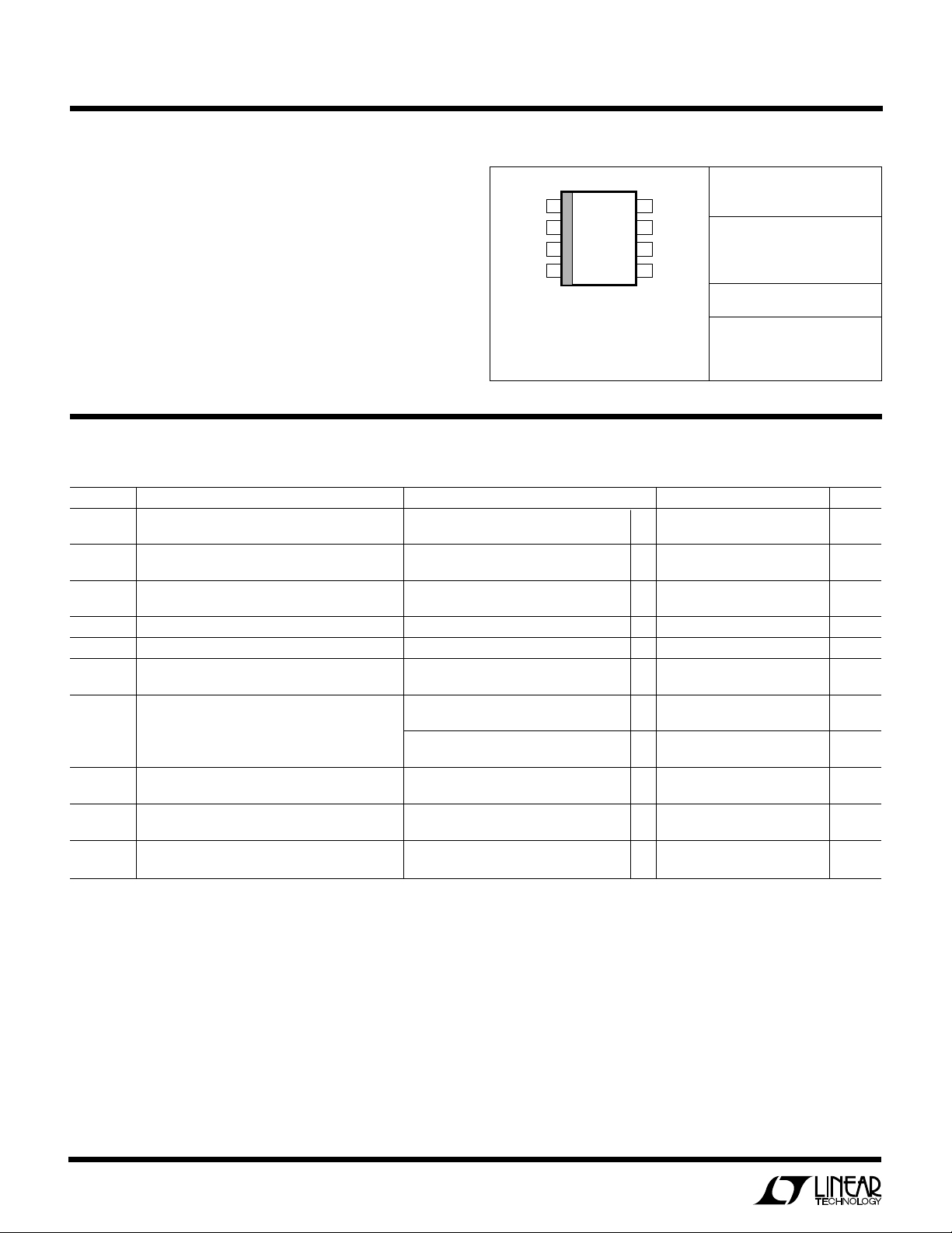
PACKAGE/ORDER INFORMATION
(Note 1)
Supply Voltage ........................................................ 13V
Input Voltages ...........................................–0.3V to 13V
Output Voltages ......................................... –0.3V to 13V
Output Short Circuit Duration ..........................Indefinite
Operating Temperature Range ..................... 0°C to 70°C
Storage Temperature Range (Note 2) ... –65°C to 150°C
Lead Temperature (Soldering, 10 sec).................. 300°C
TOP VIEW
OUT
1
IN
2
NC*
3
GND
4
S8 PACKAGE
8-LEAD PLASTIC SO
T
= 125°C, θJA = 190°C/W
JMAX
*CONNECTED INTERNALLY.
DO NOT CONNECT EXTERNAL
CIRCUITRY TO THESE PINS.
Consult factory for Industrial and Military grade parts.
NC*
8
NC*
7
NC*
6
NC*
5
ORDER PART
NUMBER
LTC1258CS8-3
LTC1258CS8-4.1
S8 PART MARKING
12583
125841
ELECTRICAL CHARACTERISTICS
VIN = 3.2V (LTC1258-3), VIN = 4.3 (LTC1258-4.1), I
SYMBOL PARAMETER CONDITIONS MIN TYP MAX UNITS
V
IN
I
IN
V
OUT
e
n
TC Output Voltage Temp Coefficient (Note 5) T
V
OUT/VIN
V
OUT/IOUT
I
SC
∆V
DO
V
HYST
Input Voltage Range LTC1258-3 ● 3.2 12.6 V
Input Current 6.5 µA
Output Voltage (Note 3) LTC1258-3 2.9955 3 3.0045 V
Output Voltage Noise (Note 4) 0.1Hz ≤ f ≤ 10Hz 40 µVp-p
Line Regulation VIN = 3.2V to 12.6V (LTC1258-3) ● 75 150 µV/V
Load Regulation (Note 6) Sourcing 0mA to 10mA 0.1 0.2 mV/mA
Short-Circuit Output Current V
Dropout Voltage (Note 7) I
Output Hysteresis (Note 8) ∆T = –40°C to 85°C 200 ppm
= 0mA, TA = 25°C unless otherwise noted.
OUT
LTC1258-4.1 ● 4.3 12.6 V
● 8.5 µA
LTC1258-4.1 4.090 4.096 4.102 V
≤ TJ ≤ T
MIN
VIN = 4.3V to 12.6V (LTC1258-4.1) ● 75 150 µV/V
Sinking 0mA to 2mA 1.75 4.0 mV/mA
OUT
V
OUT
= 0, ∆V
OUT
I
= 10mA, ∆V
OUT
∆T = 0°C to 70°C 50 ppm
MAX
Shorted to GND 20 40 60 mA
Shorted to V
IN
≤ 0.1% ● 100 mV
OUT
≤ 0.1% ● 200 mV
OUT
● 15 40 ppm/°C
● 0.3 mV/mA
● 6.5 mV/mA
2 4 15 mA
U
The ● denotes specifications which apply over the full operating
temperature range.
Note 1: Absolute Maximum Ratings are those values beyond which the life
of a device may be impaired.
Note 2: If the part is stored outside of the specified operating temperature
range, the output may shift due to hysteresis.
Note 3: ESD (Electrostatic Discharge) sensitive device. Extensive use of
ESD protection devices are used internal to the LTC1258-3/LTC1258-4.1,
however, high electrostatic discharge can damage or degrade the device.
Use proper ESD handling precautions.
Note 4: Peak-to-peak noise is measured with a single highpass filter at
0.1Hz and 2-pole lowpass filter at 10Hz.
Note 5: Temperature coefficient is measured by dividing the change in
output voltage by the specified operating temperature range.
2
Note 6: Load regulation is measured on a pulse basis from no load to the
specified load current. Output changes due to die temperature change
must be taken into account separately.
– V
Note 7: Dropout voltage is (V
nominal value at V
Note 8: Hysteresis in output voltage is created by package stress that
differs depending on whether the IC was previously at a higher or lower
temperature. Output voltage is always measured at 25°C, but the IC is
cycled to 85°C or –40°C before successive measurements. Hysteresis is
roughly proportional to the square of the temperature change. Hysteresis
is not normally a problem for operational temperature excursions where
the instrument might be stored at high or low temperature.
IN
= V
OUT
IN
+ 0.5V.
OUT
) when V
falls to 0.1% below its
OUT

UUU
PIN FUNCTIONS
LTC1258-3/LTC1258-4.1
OUT (Pin 1): Reference Output. The output can source up
to 10mA and sink up to 2mA. Stable with output bypass
capacitor ranges from 0µF to 1µF.
IN (Pin 2): Positive Supply. Bypass with a 0.1µ F capacitor
is recommended if the output loading changes.
(V
+ 0.2V) ≤ VIN ≤ 12.6V.
OUT
W
BLOCK DIAGRAM
2
IN
+
2.424V
–
R2
GND
4
NC (Pins 3, 5, 6, 7, 8): No Connection. Connected
internally for post package trim. These pins should be left
unconnected.
GND (Pin 4): Negative Supply or Ground Connection.
1
OUT
R1
1258-3/4.1 BD
U
WUU
APPLICATIONS INFORMATION
Longer Battery Life
Series references have an advantage over shunt style
references. To operate, shunt references require a resistor
between the power supply and the output. This resistor
must be chosen to supply the maximum current that is
demanded by the circuit being regulated. When the circuit
being controlled is not operating at this maximum current,
the shunt reference must always sink this current, resulting in high power dissipation and short battery life.
1mA
I
OUT
0mA
V
OUT
100mV/DIV
10ms/DIV
The LTC1258-3/LTC1258-4.1 series low dropout references do not require a current setting resistor and can
operate with any supply voltage from (V
+ 0.2V) to
OUT
12.6V. When the circuitry being regulated does not demand current, the LTC1258-3/LTC1258-4.1 reduces its
dissipation and battery life is extended. If the reference is
not delivering load current it dissipates only 13.2µ W on a
3.3V supply (LTC1258-3), yet the same connection can
deliver 10mA of load current when demanded.
1mA
I
OUT
0mA
V
OUT
100mV/DIV
0.5ms/DIV
Figure 1. Reference Output Load Transient Response
3

LTC1258-3/LTC1258-4.1
U
WUU
APPLICATIONS INFORMATION
Output Bypass Capacitor
The LTC1258-3/LTC1258-4.1 are designed to be stable
with or without capacitive loads. With no capacitive load,
the reference is ideal for fast settling applications, or
where PC board space is a premium.
In applications with significant output loading changes, an
output bypass capacitor of up to 1µF can be used to
improve the output transient response. Figure 1 shows the
response of the reference to a 1mA to 0µA load step with
a 1µ F output capacitor. If more than 1µ F of output capacitance is required, a resistor in series with the capacitor is
recommended to reduce the output ringing. Figure 2
shows the resistor and capacitor values required to achieve
critical damping.
Internal P-Channel Pass Transistor
The LTC1258-3/LTC1258-4.1 feature an internal P-channel MOSFET pass transistor. This provides several advantages over similar designs using a PNP bipolar pass
transistor.
The LTC1258-3/LTC1258-4.1 consume only 4µ A of quiescent current under light and heavy loads as well as in
dropout; whereas, PNP based references waste considerable amounts of current when the pass transistor is
saturated. In addition, the LTC1258-3/LTC1258-4.1 provide a lower dropout voltage (200mV max) than PNP
based references.
10k
1k
100
RESISTOR VALUE (Ω)
10
1
Figure 2. Damping Resistance vs Output Capacitor Value
10 100 1k
OUTPUT CAPACITOR VALUE (µF)
1258-3/4.1 F02
U
TYPICAL APPLICATIONS
Micropower Low Dropout Negative Reference
0.2V ≤ V
V
= –3V
OUT
1258-3/4.1 TA03
CC
2
–
1/2 LTC1542
3
+
= –4V
V
SS
2
IN
LTC1258-3
1
OUT
8
4
0.1µF
1
GND
4
≤ 8.5V
VCC = 9V
Supply Splitter
LTC1258-4.1
2
0.1µF 0.1µF
GND
4
1
OUTIN
4.096V
VIRTUAL
GROUND
1258-3/4.1 TA04
RELATED PARTS
PART NUMBER DESCRIPTION COMMENTS
LT®1634 Micropower Precision Shunt Voltage Reference 0.05% Max, 25ppm/°C Max Drift, 1.25V, 2.5V, 4.096V and 5V Outputs
LT1460 Micropower Series Reference 0.075% Max, 10ppm/°C Max Drift, 2.5V, 5V and 10V Outputs
LTC1440 Micropower Comparator with Reference 3.7µA Max ICC, 1% 1.182V Reference, Adjustable Hysteresis
LTC1540 Nanopower Comparator with Reference 600nA Max ICC, 2% 1.182V Reference, Adjustable Hysteresis
4
Linear T echnolog y Corporation
1630 McCarthy Blvd., Milpitas, CA 95035-7417
(408) 432-1900 ● FAX: (408) 434-0507
●
www.linear-tech.com
12585i LT/TP 1198 4K • PRINTED IN USA
LINEAR TECHNOLOGY CORPORATION 1998
 Loading...