

LTC1155
Dual High Side
Micropower MOSFET Driver
EATU
F
■
Fully Enhances N-Channel Power MOSFETs
■
8µA Standby Current
■
85µA ON Current
■
Short-Circuit Protection
■
Wide Power Supply Range: 4.5V to 18V
■
Controlled Switching ON and OFF Times
■
No External Charge Pump Components
■
Replaces P-Channel High Side MOSFETs
■
Compatible with Standard Logic Families
■
Available in 8-Pin SO Package
PPLICATI
A
■
Laptop Power Bus Switching
■
SCSI Termination Power Switching
■
Cellular Phone Power Management
■
P-Channel Switch Replacement
■
Relay and Solenoid Drivers
■
Low Frequency Half H-Bridge
■
Motor Speed and Torque Control
RE
S
O
U
S
DUESCRIPTIO
The LTC®1155 dual high side gate driver allows using low
cost N-channel FETs for high side switching applications.
An internal charge pump boosts the gate above the positive rail, fully enhancing an N-channel MOSFET with no
external components. Micropower operation, with 8µA
standby current and 85µA operating current, allows use in
virtually all systems with maximum efficiency.
Included on-chip is overcurrent sensing to provide automatic shutdown in case of short circuits. A time delay can
be added in series with the current sense to prevent false
triggering on high in-rush loads such as capacitors and
incandescent lamps.
The LTC1155 operates off of a 4.5V to 18V supply input
and safely drives the gates of virtually all FETs. The
LTC1155 is well suited for low voltage (battery-powered)
applications, particularly where micropower “sleep” operation is required.
The LTC1155 is available in both 8-pin PDIP and 8-pin SO
packages.
, LTC and LT are registered trademarks of Linear Technology Corporation.
U
O
A
PPLICATITYPICAL
Laptop Computer Power Bus Switch with Short Circuit Protection
VS = 4.5V TO 5.5V
+
DS2V
S
G2
IN2
*SURFACE MOUNT
10µF
TTL, CMOS INPUT
DISK
DRIVE
DISPLAY
MAX
5A
R
SEN
0.02Ω
R
DLY
100k
*IRLR034
TTL, CMOS INPUT
POWER BUS
SYSTEM
C
DLY
0.1µF
DS1
G1
LTC1155
IN1
GND
µP
GND
C
DLY
0.1µF
R
DLY
100k
*IRLR034
PRINTER,
ETC.
R
SEN
0.02Ω
5A
MAX
1155 TA01
Switch Voltage Drop
0.25
0.20
0.15
0.10
VOLTAGE DROP (V)
0.05
0.00
0
123
OUTPUT CURRENT (A)
1155 TA02
1
LTC1155
A
W
O
LUTEXI T
S
A
WUW
ARB
U
G
I
(Note 1)
S
Supply Voltage ........................................................ 22V
Input Voltage ...................... (VS +0.3V) to (GND – 0.3V)
Gate Voltage .........................(VS +24V) to (GND – 0.3V)
Current (Any Pin).................................................. 50mA
Storage Temperature Range ................. – 65°C to 150°C
WU
/
PACKAGE
1
DS1
2
G1
3
GND
4
IN1
J8 PACKAGE
8-LEAD CERDIP
T
= 150°C, θJA = 100°C/W (J8)
JMAX
= 100°C, θJA = 130°C/W (N8)
T
JMAX
O
TOP VIEW
N8 PACKAGE
8-LEAD PDIP
RDER I FOR ATIO
ORDER PART
8
DS2
7
G2
6
V
S
IN2
5
NUMBER
LTC1155CN8
LTC1155CJ8
LTC1155IN8
LTC1155MJ8
Operating Temperature Range
LTC1155C................................................ 0°C to 70°C
LTC1155I........................................... –40°C to 85°C
LTC1155M........................................ – 55°C to 125°C
Lead Temperature Range (Soldering, 10 sec.)...... 300°C
U
ORDER PART
NUMBER
LTC1155CS8
LTC1155IS8
S8 PART MARKING
1155
1155I
DS1
1
G1
2
GND
3
IN1
4
S8 PACKAGE
8-LEAD PLASTIC SO
T
= 100°C, θJA = 150°C/W
JMAX
TOP VIEW
DS2
8
G2
7
V
6
S
IN2
5
LECTRICAL C CHARA TERIST
E
ICS
The ● denotes the specifications which apply over the full operating temperature range, otherwise specifications are at TA = 25°C.
VS = 4.5V to 18V, unless otherwise noted.
LTC1155M LTC1155C/LTC1155I
SYMBOL PARAMETER CONDITIONS MIN TYP MAX MIN TYP MAX UNITS
V
S
I
Q
V
INH
V
INL
I
IN
C
IN
V
SEN
I
SEN
V
GATE-VS
t
ON
Supply Voltage ● 4.5 18 4.5 18 V
Quiescent Current OFF VIN = 0V, VS = 5V (Note 2) 8 20 8 20 µA
Quiescent Current ON VS = 5V, VIN = 5V (Note 3) 85 120 85 120 µA
Quiescent Current ON VS = 12V, VIN = 5V (Note 3) 180 400 180 400 µA
Input High Voltage ● 2.0 2.0 V
Input Low Voltage ● 0.8 0.8 V
Input Current 0V < VIN < V
Input Capacitance 5 5 pF
Drain Sense Threshold Voltage 80 100 120 80 100 120 mV
Drain Sense Input Current 0V < V
Gate Voltage Above Supply VS = 5V ● 6.0 6.8 9.0 6.0 6.8 9.0 V
= 6V ● 7.5 8.5 15 7.5 8.5 15 V
V
S
VS = 12V ● 15 18 25 15 18 25 V
Turn ON Time VS = 5V, C
Time for V
Time for V
VS = 12V, C
Time for V
Time for V
SEN
S
< V
S
= 1000pF
GATE
> VS + 2V 50 250 750 50 250 750 µs
GATE
> VS + 5V 200 1100 2000 200 1100 2000 µs
GATE
= 1000pF
GATE
> VS + 5V 50 180 500 50 180 500 µs
GATE
> VS + 10V 120 450 1200 120 450 1200 µs
GATE
● ±1.0 ±1.0 µA
● 75 100 125 75 100 125 mV
±0.1 ±0.1 µA
2
LTC1155
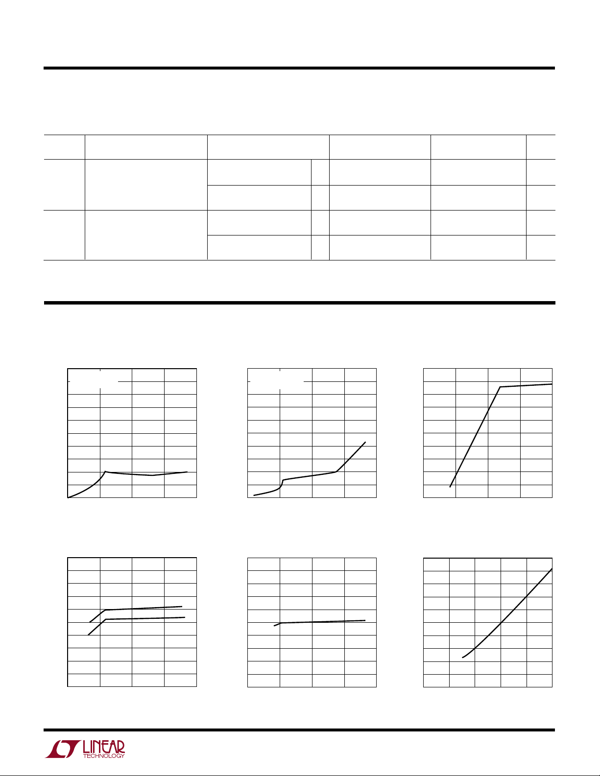
SUPPLY VOLTAGE (V)
0
4
V – V (V)
16
18
20
22
24
510 20
1155 TPC03
6
8
10
12
14
15
S
GATE
SUPPLY VOLTAGE (V)
0
0
V
GATE
(V)
18
21
24
27
30
24 10
1155 G06
3
6
9
12
15
6
8
LECTRICAL C CHARA TERIST
E
The ● denotes the specifications which apply over the full operating temperature range, otherwise specifications are at TA = 25°C.
VS = 4.5V to 18V, unless otherwise noted.
SYMBOL PARAMETER CONDITIONS MIN TYP MAX MIN TYP MAX UNITS
t
OFF
t
SC
Turn OFF Time VS = 5V, C
Short-Circuit Turn OFF Time VS = 5V, C
ICS
Time for V
VS = 12V, C
Time for V
Time for V
VS = 12V, C
Time for V
LTC1155M LTC1155C/LTC1155I
= 1000pF
GATE
< 1V 10 36 60 10 36 60 µs
GATE
= 1000pF
GATE
< 1V 10 26 60 10 26 60 µs
GATE
= 1000pF
GATE
< 1V 5 16 30 5 16 30 µs
GATE
= 1000pF
GATE
< 1V 5 16 30 5 16 30 µs
GATE
Note 1: Absolute Maximum Ratings are those values beyond which the life
of a device may be impaired.
Note 2: Quiescent current OFF is for both channels in OFF condition.
Note 3: Quiescent current ON is per driver and is measured independently.
UW
LPER
F
O
R
ATYPICA
Standby Supply Current Supply Current/Side (ON) High Side Gate Voltage
50
V
= V
= 0V
IN1
0
IN2
= 25°C
T
J
510 20
SUPPLY VOLTAGE (V)
15
1155 G01
45
40
35
µ
30
25
20
15
SUPPLY CURRENT ( A)
10
5
0
Input Threshold Voltage Drain Sense Threshold Voltage Low Side Gate Voltage
2.4
2.2
2.0
1.8
1.6
1.4
1.2
1.0
0.8
INPUT THRESHOLD VOLTAGE (V)
0.6
0.4
0
V
ON
V
OFF
15
1155 G04
510 20
SUPPLY VOLTAGE (V)
CCHARA TERIST
E
C
1000
V
OR V
IN1
900
= 25°C
T
J
800
700
µ
600
500
400
300
SUPPLY CURRENT ( A)
200
100
0
0
150
140
130
120
110
100
90
80
70
60
DRAIN SENSE THRESHOLD VOLTAGE (V)
50
0
510 20
510 20
ICS
= 2V
IN2
SUPPLY VOLTAGE (V)
SUPPLY VOLTAGE (V)
15
1155 G02
15
1155 G05
3
LTC1155
SUPPLY VOLTAGE (V)
0
0
TURN-OFF TIME (µs)
30
35
40
45
50
510 20
1155 G09
5
10
15
20
25
15
V
SEN
= VS –1V
NO EXTERNAL DELAY
C
GATE
= 1000pF
TIME FOR V
GATE
< 1V
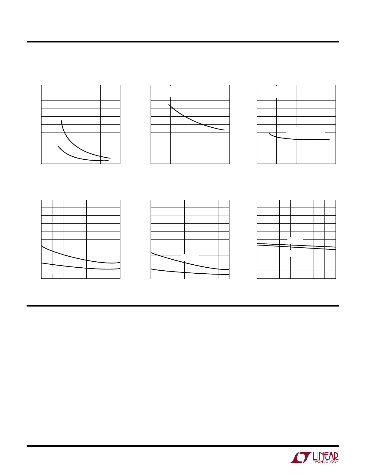
UW
Y
PICA
1000
900
800
700
600
500
400
TURN-ON TIME (µs)
300
200
100
0
50
45
40
35
30
25
20
15
SUPPLY CURRENT (µA)
10
5
0
–50
LPER
F
O
R
AT
CCHARA TERIST
E
C
ICS
Turn ON Time Turn OFF Time Short-Circuit Turn OFF Delay Time
C
= 1000pF
GATE
VGS = 5V
V
= 2V
GS
0
510 20
SUPPLY VOLTAGE (V)
15
1155 G07
50
C
= 100pF
GATE
45
TIME FOR V
40
35
µ
30
25
20
TURN OFF TIME ( s)
15
10
5
0
0
< 1V
GATE
510 20
SUPPLY VOLTAGE (V)
15
1155 G08
Standby Supply Current Supply Current Per Side (ON) Input ON Threshold
2.4
2.2
2.0
1.8
1.6
1.4
1.2
1.0
INPUT THRESHOLD (V)
0.8
0.6
0.4
–50
–25 0 25 50
TEMPERATURE (°C)
VS = 5V
VS = 18V
VS = 18V
VS = 5V
–25 0 25 50
TEMPERATURE (°C)
75 100 125
1155 G10
1000
900
800
700
600
500
400
300
SUPPLY CURRENT (µA)
200
100
VS = 5V
0
–50
–25 0 25 50
VS = 12V
75 100 125
TEMPERATURE (°C)
1155 G11
75 100 125
1155 G12
UUU
PIN FUNCTIONS
Input Pin
The LTC1155 logic input is a high impedance CMOS gate
and should be grounded when not in use. These input pins
have ESD protection diodes to ground and supply and,
therefore, should not be forced beyond the power supply
rails.
Gate Drive Pin
The gate drive pin is either driven to ground when the
switch is turned OFF or driven above the supply rail when
the switch is turned ON. This pin is a relatively high
impedance when driven above the rail (the equivalent of a
4
few hundred kΩ). Care should be taken to minimize any
loading of this pin by parasitic resistance to ground or
supply.
Supply Pin
The supply pin of the LTC1155 serves two vital purposes.
The first is obvious: it powers the input, gate drive,
regulation and protection circuitry. The second purpose is
less obvious: it provides a Kelvin connection to the top of
the two drain sense resistors for the internal 100mV
reference. The supply pin should be connected directly to
the power supply source as close as possible to the top of
the two sense resistors.
UUU
PIN FUNCTIONS
LTC1155
The supply pin of the LTC1155 should not be forced below
ground as this may result in permanent damage to the
device. A 300Ω resistor should be inserted in series with
the ground pin if negative supply voltages are anticipated.
Drain Sense Pin
As noted previously, the drain sense pin is compared
against the supply pin voltage. If the voltage at this pin is
more than 100mV below the supply pin, the input latch will
be reset and the MOSFET gate will be quickly discharged.
Cycle the input to reset the short-circuit latch and turn the
MOSFET back on.
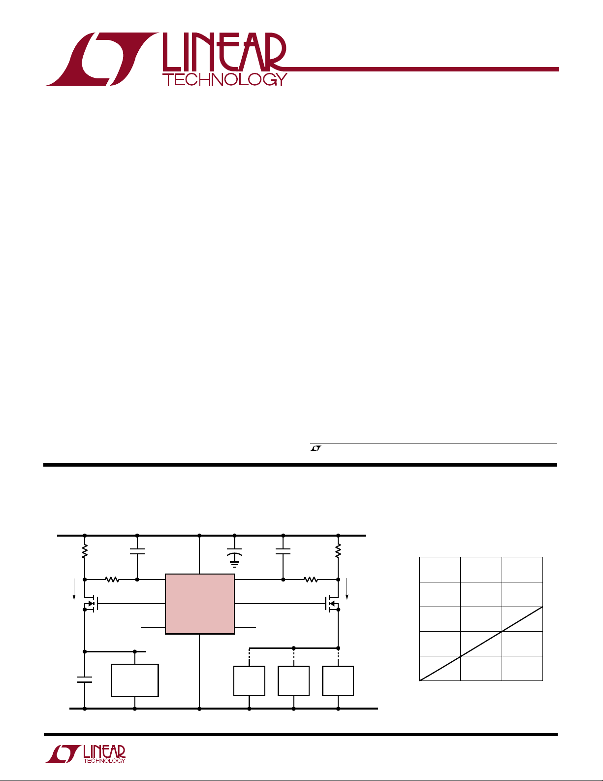
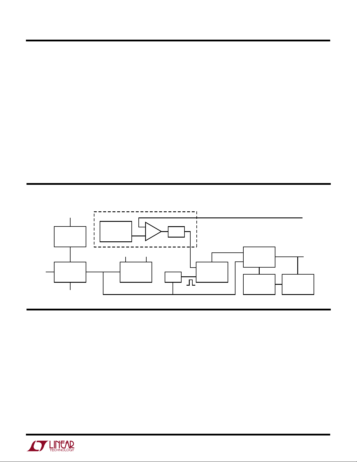
W
BLOCK
IDAGRA
V
S
LOW STANDBY
CURRENT
REGULATOR
ANALOG SECTION
100mV
REFERENCE
COMP
10µs
DELAY
This pin is also a high impedance CMOS gate with ESD
protection and, therefore, should not be forced beyond the
power supply rails. To defeat the over current protection,
short the drain sense to supply.
Some loads, such as large supply capacitors, lamps or
motors require high inrush currents. An RC time delay
must be added between the sense resistor and the drain
sense pin to ensure that the drain sense circuitry does not
false trigger during start-up. This time constant can be set
from a few microseconds to many seconds. However, very
long delays may put the MOSFET in risk of being destroyed
by a short-circuit condition (see Applications Information
section).
DRAIN
SENSE
ANALOG DIGITAL
IN
TTL-TO-CMOS
CONVERTER
GND
VOLTAGE
REGULATORS
ONE
SHOT
U
OPERATIO
The LTC1155 contains two independent power MOSFET
gate drivers and protection circuits (refer to the Block
Diagram for details). Each half of the LTC1155 consists of
the following functional blocks:
TTL and CMOS Compatible Inputs
Each driver input has been designed to accommodate a
wide range of logic families. The input threshold is set at
1.3V with approximately 100mV of hysteresis.
A voltage regulator with low standby current provides
continuous bias for the TTL to CMOS converters. The TTL
GATE CHARGE
AND DISCHARGE
CONTROL LOGIC
R
INPUT
LATCH
S
OSCILLATOR
AND CHARGE
PUMP
GATE CHARGE
GATE
FAST/SLOW
LOGIC
1155 BD
to CMOS converter output enables the rest of the circuitry.
In this way the power consumption is kept to a minimum
in the standby mode.
Internal Voltage Regulation
The output of the TTL to CMOS converter drives two
regulated supplies which power the low voltage CMOS
logic and analog blocks. The regulator outputs are isolated
from each other so that the noise generated by the charge
pump logic is not coupled into the 100mV reference or the
analog comparator.
5

LTC1155
OPERATIO
U
Gate Charge Pump
Gate drive for the power MOSFET is produced by an
adaptive charge pump circuit that generates a gate voltage
substantially higher than the power supply voltage. The
charge pump capacitors are included on-chip and, therefore, no external components are required to generate the
gate drive.
Drain Current Sense
The LTC1155 is configured to sense the drain current of
the power MOSFET in high side applications. An internal
100mV reference is compared to the drop across a sense
resistor (typically 0.002Ω to 0.1Ω) in series with the drain
PPLICATI
A
U
O
S
I FOR ATIO
WU
U
Protecting the MOSFET
The MOSFET is protected against destruction by removing
drive from the gate as soon as an overcurrent condition is
detected. Resistive and inductive loads can be protected
with no external time delay. Large capacitive or lamp
loads, however, require that the overcurrent shutdown
function be delayed long enough to start the load but short
enough to ensure the safety of the MOSFET.
lead. If the drop across this resistor exceeds the internal
100mV threshold, the input latch is reset and the gate is
quickly discharged by a large N-channel transistor.
Controlled Gate Rise and Fall Times
When the input is switched ON and OFF, the gate is
charged by the internal charge pump and discharged in a
controlled manner. The charge and discharge rates have
been set to minimize RFI and EMI emissions in normal
operation. If a short circuit or current overload condition
is encountered, the gate is discharged very quickly (typically a few microseconds) by a large N-channel transistor.
VS = 5.0V
R
SEN
0.03Ω
IRLZ34
IN1
V
S
LTC1155
GND
DS1
G1
C
DLY
0.22µF
R
DLY
270k
Example Calculations
Consider the circuit of Figure 1. A power MOSFET is driven
by one side of an LTC1155 to switch a high inrush current
load. The drain sense resistor is selected to limit the
maximum DC current to 3.3A.
R
= V
SEN
SEN/ITRIP
= 0.1/3.3A
= 0.03Ω
A time delay is introduced between R
and the drain
SEN
sense pin of the LTC1155 which provides sufficient delay
to start a high inrush load such as large supply capacitors.
In this example circuit, we have selected the IRLZ34
because of its low R
(0.05Ω with VGS = 5V). The FET
DS(ON )
6
LOAD
GND
1155 F01
Figure 1. Adding an RC Delay
drops 0.1V at 2A and, therefore, dissipates 200mW in
normal operation (no heat sinking required).
If the output is shorted to ground, the current through the
FET rises rapidly and is limited by the R
DS(ON)
of the FET,
the drain sense resistor and the series resistance between the power supply and the FET. Series resistance in
the power supply can be substantial and attributed to
many sources including harness wiring, PCB traces,
supply capacitor ESR, transformer resistance or battery
resistance.

LTC1155
MOSFET CURRENT (1 = SET CURRENT)
1
0.01
OVERCURRENT SHUTDOWN TIME (1= RC)
0.1
1
10
5 10 20 100
1155 F02
250
PPLICATI
A
U
O
S
I FOR ATIO
WU
U
For this example, we assume a worst-case scenario; i.e.,
that the power supply to the power MOSFET is “hard” and
provides a constant 5V regardless of the current. In this
case, the current is limited by the R
of the MOSFET
DS(ON)
and the drain sense resistance. Therefore:
I
PEAK
= V
SUPPLY
/0.08Ω
= 62.5A
The drop across the drain sense resistor under these
conditions is much larger than 100mV and is equal to the
drain current times the sense resistance:
V
DROP
= (I
PEAK
)(R
SEN
)
= 1.88V
By consulting the power MOSFET data sheet SOA graph,
we note that the IRLZ34 is capable of delivering 62.5A at
a drain-to-source voltage of 3.12V for approximately
10ms.
Graphical Approach to Selecting R
DLY
and C
DLY
Figure 2 is a graph of normalized overcurrent shutdown
time versus normalized MOSFET current. This graph can
be used instead of the above equation to calculate the RC
time constant. The Y axis of the graph is normalized to one
RC time constant. The X axis is normalized to the set
current. (The set current is defined as the current required
to develop 100mV across the drain sense resistor).
An RC time constant can now be calculated which satisfies
this requirement:
t
RC
RC
=
=
=
=
In
In
–. /–.
0 01 0 054
182
–
V
1
1
−
−
SEN
RI
•
SEN MAX
–.
001
.
010
•
..
0 030 62 5
ms
This time constant should be viewed as a maximum safe
delay time and should be reduced if the competing
requirement of starting a high inrush current load is less
stringent; i.e., if the inrush time period is calculated at
20ms, the RC time constant should be set at roughly two
or three times this time period and not at the maximum of
182ms. A 60ms time constant would be produced with a
270k resistor and a 0.22µF capacitor (as shown in
Figure 1).
Figure 2. Shutdown Time vs MOSFET Current
Note that the shutdown time is shorter for increasing
levels of MOSFET current. This ensures that the total
energy dissipated by the MOSFET is always within the
bounds established by the MOSFET manufacturer for safe
operation.
In the example presented above, we established that the
power MOSFET should not be allowed to pass 62.5A for
more than 10ms. 62.5A is roughly 18 times the set current
of 3.3A. By drawing a line up from 18 and reflecting it off
the curve, we establish that the RC time constant should
be set at 10ms divided by 0.054, or 180ms. Both methods
result in the same conclusion.
Using a Speed Up Diode
A way to further reduce the amount of time that the power
MOSFET is in a short-circuit condition is to “bypass”the
delay resistor with a small signal diode as shown in Figure
3. The diode will engage when the drop across the drain
sense resistor exceeds 0.7V, providing a direct path to the
7

LTC1155
PPLICATI
A
U
O
S
I FOR ATIO
VS = 5.0V
V
S
DS1
IN1
LTC1155
GND
Figure 3. Using a Speed-Up Diode
G1
GND
WU
C
DLY
0.22µF
R
270k
1N4148
DLY
D1
R
0.025Ω
IRLZ34
LOAD
1155 F03
U
SEN
sense pin and dramatically reducing the amount of time
the MOSFET is in an overload condition. The drain sense
resistor value is selected to limit the maximum DC current
to 4A. Above 28A, the delay time drops to 10µs.
Switched Supply Applications
If the MOSFET is turned ON and the power supply (battery)
removed, the inductor current is delivered by the supply
capacitor. The supply capacitor must be large enough to
deliver the energy demanded by the discharging inductor.
If the storage capacitor is too small, the supply lead of the
LTC1155 may be pulled below ground, permanently
destroying the device.
Consider the case of a load inductance of 1mH which is
supporting 3A when the 6V power supply connection is
interrupted. A supply capacitor of at least 250µF is
required to prevent the supply lead of the LTC1155 from
being pulled below ground (along with any other circuitry
tied to the supply).
Any wire between the power MOSFET source and the load
will add a small amount of parasitic inductance in series
with the load (approximately 0.4µH/foot). Bypass the
power supply lead of the LTC1155 with a minimum of
10µF to ensure that this parasitic load inductance is
discharged safely, even if the load is otherwise resistive.
Large inductive loads, such as solenoids, relays and
motors store energy which must be directed back to either
the power supply or to ground when the supply voltage is
interrupted (see Figure 4). In normal operation, when the
switch is turned OFF, the energy stored in the inductor is
harmlessly absorbed by the MOSFET; i.e., the current
flows out of the supply through the MOSFET until the
inductor current falls to zero.
+
IN1
+
C
S
V
S
DS1
LTC1155
GND
Figure 4. Switched Supply
G1
GND
C
DLY
R
DLY
R
SEN
0.025Ω
IRLZ34
L
LOAD
1155 F04
Large Inductive Loads
Large inductive loads (>0.1mH) may require diodes connected directly across the inductor to safely divert the
stored energy to ground. Many inductive loads have these
diodes included. If not, a diode of the proper current rating
should be connected across the load to safely divert the
stored energy.
Reverse-Battery Protection
The LTC1155 can be protected against reverse-battery
conditions by connecting a resistor in series with the
ground lead as shown in Figure 5. The resistor limits the
supply current to less than 50mA with –12V applied. Since
the LTC1155 draws very little current while in normal
operation, the drop across the ground resistor is minimal.
The TTL or CMOS driving logic is protected against
reverse-battery conditions by the 100k input current limiting resistor. The addition of 100k resistance in series
with the input pin will not affect the turn ON and turn OFF
times which are dominated by the controlled gate charge
and discharge periods.
8

LTC1155
PPLICATI
A
100k
5V
IN1
GND
O
V
S
LTC1155
GND
U
S
I FOR ATIO
VS = 4.5V TO 18V
C
DLY
DS1
G1
300Ω
1/4W
WU
R
DLY
+
10µF
25V
LOAD
U
R
SEN
1155 F05
Figure 5. Reverse Battery Protection
Overvoltage Protection
The MOSFET and load can be protected against overvoltage conditions by using the circuit of Figure 6. The drain
sense function is used to detect an overvoltage condition
and quickly discharge the power MOSFET gate. The 18V
zener diode conducts when the supply voltage exceeds
18.6V and pulls the drain sense pin 0.6V below the supply
pin voltage.
The supply voltage is limited to 18.6V and the gate drive is
immediately removed from the MOSFET to ensure that it
cannot conduct during the overvoltage period. The gate of
the MOSFET will be latched OFF until the supply transient
is removed and the input turned OFF and ON again.
VS = 4.5V TO 18V
510Ω
V
S
IN1
LTC1155
GND
GND
Figure 6. Overvoltage Shutdown and Protection
10k 1N4148
DS1
G1
18V
LOAD
1155 F06
U
O
PPLICATITYPICAL
LMC555
ALL COMPONENTS SHOWN ARE SURFACE MOUNT
SA
+
84
1
f
O
3
2
6
10µF
= 1Hz
750k
Dual 2A Autoreset Electronic Fuse
5V
100k
0.1µF
30k
G1
IN1
DS1
S
LTC1155
GND
0.03Ω
1/2 SI9956DY
1N4148
1N4148
OUT 1 OUT 2
1.0µF
0.1µF
30k
DS2V
G2
IN2
0.03Ω
1/2 SI9956DY
100k
1155 TA03
9

LTC1155
U
O
PPLICATITYPICAL
SA
X-NOR Fault DetectionHigh Side Driver with VDS Sense Short-Circuit Shutdown
4.5V TO 6V
+
10µF
V
5V
*
*ANY 74C OR 74HC LOGIC GATE.
MOSFET SHUTS DOWN IF V
IN1
0.01µF
S
1/2
LTC1155
GND
4.5V TO 6V
+
30k
DS1
G1
270k
> 1V
DS
IRLZ24
LOAD
1155 TA04
10µF
IN1
V
S
1/2
LTC1155
GND
DS1
G1
74C266
100k
FAULT
0.1Ω
10k
IRLD024
LOAD
1155 TA05
Truth Table
IN OUT CONDITION FLT
0 0 Switch OFF 1
1 0 Short Circuit 0
0 1 Open Load 0
1 1 Switch ON 1
Low Side Driver with Drain End Current Sensing Low Side Driver with Source End Current Sensing
IN1
5V
V
S
1/2
LTC1155
GND
DS1
G1
51Ω
< 60µA)
Q
6
51Ω
7
LT®1077*
4
5V
+
10µF
IN1
V
S
1/2
LTC1155
GND
DS1
G1
0.05Ω
5%
LOAD
SMP25N05
1155 TA06
+
10µF
*DO NOT SUBSTITUTE. MUST BE A PRECISION, SINGLE
SUPPLY, MICROPOWER OP AMP (I
V
LOAD
LOAD
3
+
2
–
SMP25N05
0.02Ω
5%
1155 TA07
10

LTC1155
1155 TA11
1/2
LTC1155
GND
G1
DS1
V
S
IN1
9V TO 18V
0.01Ω
IRFZ44
RISE AND FALL TIMES ARE βETA TIMES FASTER
30k
µP OR
CMOS/TTL
LOGIC
2N2222
V
GATE
= 2VS – 0.6V
1N41480.01µF
0.1µF
LOAD
5V
18V
2N3906
1155 TA09
1/2
LTC1155
GND
G1
DS1
V
S
IN1
5.2V TO 6V
0.02Ω
10µF
IRLR024
*CAPACITOR ESR SHOULD BE LESS THAN 0.5Ω
300k
0.1µF
ON/OFF
100k
0.1µF
200pF
10k
1
3
4
56
7
8
LT1431
5V/3A
470µF*
FAULT
+
+
U
O
PPLICATITYPICAL
SA
Automotive High Side Driver with Reverse-Battery
and High Voltage Transient Protection
9V TO 16V
+
10µF
V
5V
100k*
*PROTECTS TTL/CMOS GATES DURING HIGH VOLTAGE
TRANSIENT OR REVERSE BATTERY
**NOT REQUIRED FOR INDUCTIVE OR RESISTIVE LOADS
IN1
S
1/2
LTC1155
GND
300Ω
1/4W
DS1
18V
1N4746A
G1
**
C
DLY
R
DLY
18V
1N4746A
M
**
0.02Ω
5%
MTP50N05E
VALVE,
ETC.
1155 TA08
5V/3A Extremely Low Voltage Drop Regulator with 10µA Standby
Current and Short-Circuit Protection
Using the Second Channel for Fault Detection Bootstrapped Gate Drive for (100Hz < FO < 10kHz)
+
100k
1N4148
1N4148
µP OR
CONTROL
LOGIC
ON/OFF
NOTE:
DRAIN SENSE 2 IS USED TO DETECT A FAULT IN CHANNEL 1.
GATE 2 PULLS DOWN ON DRAIN SENSE 1 TO DISCHARGE
THE MOSFET AND REPORT THE FAULT TO THE µP
*NOT REQUIRED FOR RESISTIVE OR INDUCTIVE LOADS
10µF
100k
DS1FLT
G2
IN2
IN1
4.5V TO 5.5V
S
LTC1155
GND
0.1µF*
DS2V
G1
0.05Ω
30k*
SMD25N05-45L
LOAD
1155 TA10
11

LTC1155
U
O
PPLICATITYPICAL
SA
Logic Controlled Boost Mode Switching Regulator with Short-Circuit Protection and 8µA Standby Current
4.75V TO 5.25V
+
100µF
FROM µP, ETC.
FAULT
*COILTRONICS CTX-7-52
IN1
1N4148
V
S
1/2
LTC1155
GND
68µF
DS1
G1
+
0.33µF
100k
1
1k
1µF
MTM25N05L
5
LT1170
3
0.02Ω
50µH*
1N5820
4
2
High Efficiency 60Hz Full-Wave Synchronous Rectifier
10.7k
1%
1.24k
1%
5V SWITCHED
12V/1A
+
2200µF
1155 TA12
100k
10k
110V AC
12.6VCT
MOSFETs ARE SYNCHRONOUSLY ENHANCED WHEN RECTIFIER CURRENT EXCEEDS 300mA
*NO HEATSINK REQUIRED. CASES (DRAINS) CAN BE TIED TOGETHER
**INTERNAL BODY DIODE OF MOSFET
0.03Ω
10Ω
10k
–
2
3
7
LT1006
+
4
1N4001
1N4148
6
1N4148
10µF
+
1N4746A
IN1
IN2
100k
DS1
18V
S
LTC1155
GND
1N4148
DS2V
G1
G2
1N4148
18V
1N4746A
**
IRFZ44*
D
S
DS
**
IRFZ44*
9V/3A
DC
+
4700µF
16V
1155 TA13
12

LTC1155
U
O
PPLICATITYPICAL
SA
High Efficiency 60Hz Full-Wave Synchronous Rectifier
9V/3A
DC
10k
–
10k
2
3
10Ω
6.3V AC110V AC
MOSFETs ARE SYNCHRONOUSLY ENHANCED WHEN RECTIFIER CURRENT EXCEEDS 300mA
*NO HEATSINK REQUIRED
**INTERNAL BODY DIODE OF MOSFET
7
LT1006
+
4
1N4148
6
1N4148
100k
100k
IN1
IN2
DS2
S
LTC1155
GND
Push-Pull Driver with Shoot-Through Current Lockout (fO < 100Hz)
DS1V
G1
G2
18V
1N4746A
**
**
18V
1N4746A
4 × IRFZ44*
D
S
D
S
4.5V TO 6V
D
S
D
S
0.03Ω
+
**
**
4700µF
16V
1155 TA14
5V
100k
HI/LO
74HC02
*OPPOSING GATE MUST DROP BELOW 2V BEFORE THE OTHER IS CHARGED
100k
1N4148
1N4148
10µF
DS1
IN1
LTC1155
IN2
GND
0.1µF
300k
DS2V
S
G1
G2
0.01Ω
*
IRLZ24
V
*
OUT
IRFZ24
1155 TA15
13

LTC1155
U
O
PPLICATITYPICAL
SA
Full H-Bridge Driver with Shoot-Through Current Lockout and Stall Current Shutdown (fO < 100Hz)
4.5V TO 6V
10µF
DIRECTION
74HC02
DISABLE
*OPPOSING GATES ARE HELD OFF UNTIL OTHER GATES DROP BELOW 1.5V
5V
DS1
IN1
LTC1155
IN2
GND
DC Motor Speed and Torque Control for Cordless Tools and Appliances
10k
SPEED
100Ω
+
120k
47µF
16V
100k
1M
1M
+
LT1017
–
1/2
1M
1M
+
6V
ADJUST
S
+
LT1017
–
1/2
0.1µF
DS2V
G1
G2
100k
IN1
IN2
DS1
*
VN2222L
*
VN2222L
S
LTC1155
GND
0.01Ω
IRLZ44
M
IRFZ44
0.1µF
300k
DS2V
G1
G2
SMALL DC APPLIANCE
OR TOOL MOTOR
IRLZ44
IRFZ44
1155 TA16
1.1k
10k
TORQUE
ADJUST
0.1Ω
1A TO
10A
MAX
IRFZ24
M
14
0.0033µF
SPEED IS PROPORTIONAL TO PULSE WIDTH. TORQUE IS PROPORTIONAL TO CURRENT
100k
1155 TA17

PACKAGEDESCRIPTI
0.300 BSC
(0.762 BSC)
0.008 – 0.018
(0.203 – 0.457)
NOTE: LEAD DIMENSIONS APPLY TO SOLDER DIP/PLATE
OR TIN PLATE LEADS
0° – 15°
(1.143 – 1.727)
0.045 – 0.068
FULL LEAD
OPTION
CORNER LEADS OPTION
U
O
Dimensions in inches (milimeters) unless otherwise noted.
J8 Package
8-Lead CERDIP (Narrow 0.300, Hermetic)
(LTC DWG # 05-08-1110)
(4 PLCS)
0.023 – 0.045
(0.584 – 1.143)
HALF LEAD
OPTION
0.045 – 0.068
(1.143 – 1.727)
0.014 – 0.026
(0.360 – 0.660)
0.015 – 0.060
(0.381 – 1.524)
0.100 ± 0.010
(2.540 ± 0.254)
0.200
(5.080)
MAX
0.125
3.175
MIN
0.005
(0.127)
MIN
0.025
(0.635)
RAD TYP
0.405
(10.287)
MAX
87
12
LTC1155
65
0.220 – 0.310
(5.588 – 7.874)
3
4
J8 1197
0.300 – 0.325
(7.620 – 8.255)
0.065
(1.651)
0.009 – 0.015
(0.229 – 0.381)
+0.035
0.325
–0.015
+0.889
8.255
()
–0.381
*THESE DIMENSIONS DO NOT INCLUDE MOLD FLASH OR PROTRUSIONS.
MOLD FLASH OR PROTRUSIONS SHALL NOT EXCEED 0.010 INCH (0.254mm)
TYP
0.045 – 0.065
(1.143 – 1.651)
0.100 ± 0.010
(2.540 ± 0.254)
8-Lead Plastic Small Outline (Narrow 0.150)
0.010 – 0.020
(0.254 – 0.508)
0.008 – 0.010
(0.203 – 0.254)
*
DIMENSION DOES NOT INCLUDE MOLD FLASH. MOLD FLASH
SHALL NOT EXCEED 0.006" (0.152mm) PER SIDE
**
DIMENSION DOES NOT INCLUDE INTERLEAD FLASH. INTERLEAD
FLASH SHALL NOT EXCEED 0.010" (0.254mm) PER SIDE
× 45°
0.016 – 0.050
0.406 – 1.270
0.053 – 0.069
(1.346 – 1.752)
0°– 8° TYP
0.014 – 0.019
(0.355 – 0.483)
Information furnished by Linear Technology Corporation is believed to be accurate and reliable.
However, no responsibility is assumed for its use. Linear Technology Corporation makes no representation that the interconnection of its circuits as described herein will not infringe on existing patent rights.
N8 Package
8-Lead PDIP (Narrow 0.300)
(LTC DWG # 05-08-1510)
0.130 ± 0.005
(3.302 ± 0.127)
0.125
0.020
(3.175)
MIN
(0.508)
0.018 ± 0.003
(0.457 ± 0.076)
MIN
S8 Package
(LTC DWG # 05-08-1610)
0.004 – 0.010
(0.101 – 0.254)
0.050
(1.270)
TYP
0.255 ± 0.015*
(6.477 ± 0.381)
0.228 – 0.244
(5.791 – 6.197)
876
1234
0.189 – 0.197*
(4.801 – 5.004)
7
8
1
6
2
0.400*
(10.160)
MAX
3
5
N8 1197
5
0.150 – 0.157**
(3.810 – 3.988)
SO8 0996
4
15

LTC1155
PPLICATITYPICAL
6V TO 12V
U
O
SA
Isolated High Voltage High Side Switch with Circuit Breaker
1N4148
1/6 74C14
100k
100pF
0.0022µF
ON/OFF
*PICO ELECTRONICS F-28115 OR EQUIVALENT
1N4148
5V
1/6 74C14
100k
100k
1N4148
1/6 74C14
0.1µF
200V
1N5817
1k
1N5817
+
10mA
CONTROL
10µF
25V
C
4N28
BE
DS1
IN1
IN2
1M
Isolated Solid-State AC Relay with Circuit Breaker
0.1µF
1N5817
300Ω 600Ω
T1*
+
5.6V
1N4690A
1µF
100k
DS1
IN1
IN2
S
LTC1155
GND
LTC1155
GND
IN/OUT
ON/OFF
1k
90V
DS2V
G1
G2
1N4746A
0.01µF
DS2V
S
G1
G2
2N2222
18V
1N4746A
MUR420
18V
EQUIVALENT FUNCTION
18V
1N4746A
100k
2A
1k
IN/OUT
IN/OUT
24V AC
2A MAX
6A MAX
0.1Ω
M
1155 TA18
IRFZ24
0.05Ω
IRFZ24
IN/OUT
1155 TA19
RELATED PARTS
PART NUMBER DESCRIPTION COMMENTS
LTC1153 Auto-Reset Electronic Circuit Breaker Programmable Trip Current, Fault Status Output
LT1161 Quad Protected High Side MOSFET Driver 8V to 48V Supply Range, Individual Short-Circuit Protection
LTC1163 Triple 1.8V to 6V High Side MOSFET Driver 0.01µA Standby Current, Triple Driver in SO-8 Package
LTC1255 Dual 24V High Side MOSFET Driver Operates from 9V to 24V, Short-Circuit Protection
LTC1477 Protected Monolithic High Side Switch Low R
LTC1623 SMBus Dual High Side Switch Controller 2-Wire SMBus Serial Interface, Built-In Gate Charge Pumps
LTC1710 SMBus Dual Monolithic High Side Switch Two Low R
Linear Technology Corporation
16
1630 McCarthy Blvd., Milpitas, CA 95035-7417
(408) 432-1900 ● FAX: (408) 434-0507
●
www.linear-tech.com
0.07Ω Switch, 2A Short-Circuit Protected
DS(ON)
0.4Ω/300mA Switches in 8-Lead MSOP Package
DS(ON)
1155fa LT/TP 0399 2K REV A • PRINTED IN USA
LINEAR TECHNOLOGY CORPORATION 1991
 Loading...