

FEATURES
LTC1099
High Speed 8-Bit A/D
Converter with Built-In
Sample-and-Hold
U
DESCRIPTIO
■
Built-In Sample-and-Hold
■
No Missing Codes
■
No User Trims Required
■
All Timing Inputs Edge Sensitive for Easy Processor
Interface
■
Fast Conversion Time: 2.5µs
■
Latched Three-State Outputs
■
Single 5V Operation
■
No External Clock
■
Overflow Output Allows Cascading
■
TC Input Allows User Adjustable Conversion Time
■
0.3" Wide 20-Pin PDIP
U
KEY SPECIFICATIO S
■
Resolution: 8-Bits
■
Conversion Time: 2.5µs (RD Mode)
2.5µs (WR/RD Mode)
■
Slew Rate Limit (Internal S/H): 2.5V/µs
■
Low Power: 75mW Max
■
Total Unadjusted Error
LTC1099: ±1 LSB
LTC1099A: ±0.75 LSB
The LTC®1099 is a high speed microprocessor compatible
8-bit analog-to-digital converter (A/D). An internal sampleand-hold (S/H) allows the A/D to convert inputs up to the
full Nyquist limit. With a conversion rate of 2.5µs, this
allows 156kHz 5V
input signals or slew rates as high as
P-P
2.5V/µs, to be digitized without the need for an external
S/H.
Two modes of operation, Read (RD) mode and Write-Read
(WR-RD) mode, allow easy interface with processors. All
timing is internal and edge sensitive which eliminates the
need for external pulse shaping circuits. The Stand-Alone
(SA) mode is convenient for those applications not involving a processor.
Data outputs are latched with three-state control to allow
easy interface to a processor data bus or I/O port. An
overflow output (OFL) is provided to allow cascading for
higher resolution.
, LTC and LT are registered trademarks of Linear Technology Corporation.
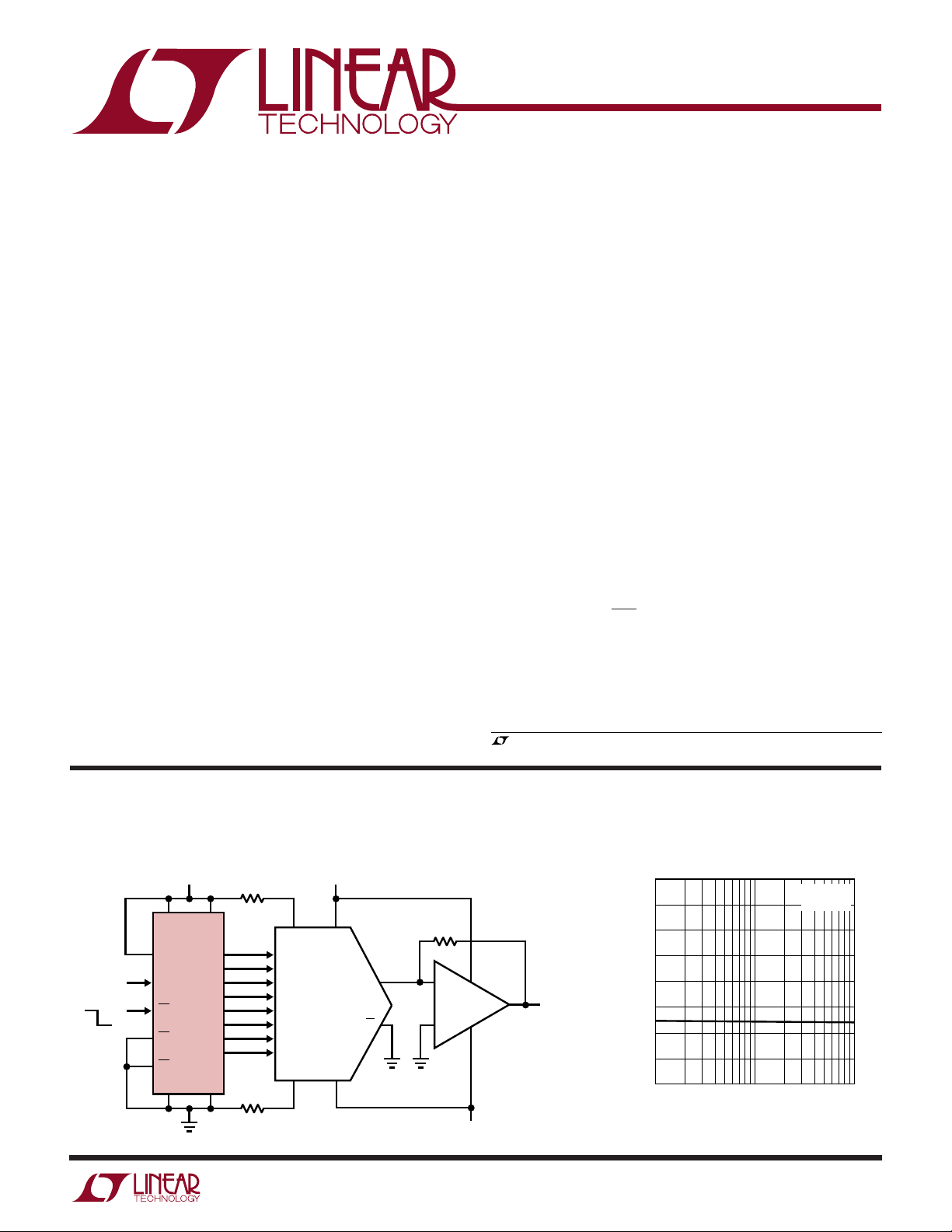
TYPICAL APPLICATION
Infinite Hold Time Sample-and-Hold (T
SAMPLE
HOLD
V
IN V
13
REF
LTC1099
7
MODE
1
IN
6
WR/RDY
8
RD
CS
GND REF
5V
12 20
+
10
V
CC
DB7
DB6
DB5
DB4
DB3
DB2
DB1
DB0
10k
14
+
REF
1
17
16
15
14
5
4
3
2
–
11
10k
2
3
4
5
6
7
8
B1
B2
B3
B4
B5
B6
B7
B8
REF
15 17
–
U
15V
V
V
= 240ns) Signal-to-Noise Ratio (SNR) vs Input Frequency
ACQ
–36
20
+
18
I
O
I
O
19
–
2.5k
2
3
7
+
LT1022AM6012
–
–15V
6
V
OUT
4
1099 TA01
–38
–40
–42
–44
–46
–48
SIGNAL-TO-NOISE RATIO, SNR (dB)
–50
–52
1
INPUT FREQUENCY (kHz)
10 100
TA = 25°C
= 2.5µs
T
C
1099 G08
1
LTC1099
V
IN
DB0
DB1
DB2
DB3
WR/RDY
MODE
RD
INT
GND
1
2
3
4
5
6
7
8
9
10
TOP VIEW
SW PACKAGE
20-LEAD PLASTIC SO
20
19
18
17
16
15
14
13
12
11
V
CC
TC
OFL
DB7
DB6
DB5
DB4
CS
REF
+
REF
–
WW
W
ABSOLUTE AXI U RATI GS
U
(Notes 1, 2)
Supply Voltage (VCC) to GND Voltage ...................... 12V
Analog and Reference Inputs... –0.3V to (VCC + 0.3V)
Digital Inputs .........................................– 0.3V to 12V
Digital Outputs ........................ –0.3V to (VCC + 0.3V)
Power Dissipation.............................................. 500mW
UUW
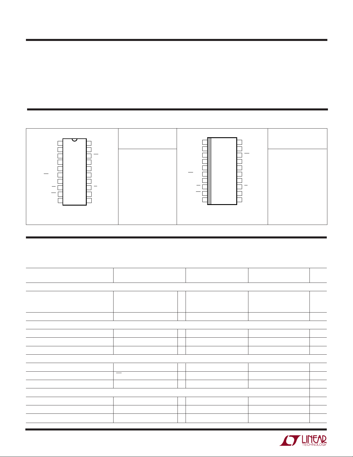
PACKAGE/ORDER I FOR ATIO
TOP VIEW
1
V
IN
2
DB0
3
DB1
4
DB2
5
DB3
6
WR/RDY
7
MODE
8
RD
9
INT
10
GND
T
= 150°C, θJA = 100°C/W
JMAX
N PACKAGE
20-LEAD PDIP
V
20
CC
T
19
C
OFL
18
DB7
17
DB6
16
DB5
15
DB4
14
CS
13
+
REF
12
–
REF
11
Consult factory for parts specified with wider operating temperature ranges.
ORDER PART
NUMBER
LTC1099CN
LTC1099ACN
LTC1099AIN
Operating Temperature Range
LTC1099C/LTC1099AC............................ 0°C to 70°C
LTC1099I/LTC1099AI ..........................–40°C to 85°C
Storage Temperature Range ................. –65°C to 150°C
Lead Temperature (Soldering, 10 sec)..................300°C
ORDER PART
NUMBER
LTC1099CSW
T
= 150°C, θJA = 130°C/W
JMAX
U
CONVERTER CHARACTERISTICS
temperature range, otherwise specifications are at TA = 25°C. VCC = 5V, REF+ = 5V, REF– = 0V and TA = T
noted.
PARAMETER CONDITIONS MIN TYP MAX MIN TYP MAX UNITS
Accuracy
Total Unadjusted Error (Note 3)
LTC1099A
LTC1099
Minimum Resolution (No Missing Codes) ● 8 8 Bits
Reference Input
Input Resistance ● 1 3.2 6 2 3.2 4.5 kΩ
REF+ Input Voltage Range (Note 4) ● REF
REF– Input Voltage Range (Note 4) ● GND REF
Analog Input
Input Voltage Range ● GND V
Input Leakage Current CS = VCC, VIN = VCC, GND ● ±3 ±3 µA
Input Capacitance 60 60 pF
Sample-and-Hold
Acquisition Time 240 240 ns
Aperture Time 110 110 ns
Tracking Rate 2.5 2.5 V/µs
2
The ● denotes the specifications which apply over the full operating
to T
MIN
LTC1099AI/LTC1099I LTC1099AC/LTC1099C
● ±0.75 ±0.75 LSB
● ±1 ±1 LSB
–
V
CC
+
CC
–
REF
GND REF
GND V
unless otherwise
MAX
V
CC
+
CC
V
V
V
LTC1099
U
DIGITAL AND DC ELECTRICAL CHARACTERISTICS
The ● denotes the specifications which apply over the full operating temperature range, otherwise specifications are at TA = 25°C.
VCC = 5V, REF+ = 5V, REF– = 0V and TA = T
SYMBOL PARAMETER CONDITIONS MIN TYP MAX MIN TYP MAX UNITS
V
IH
V
IL
I
IH
I
IL
V
OH
V
OL
I
OZ
I
SOURCE
I
SINK
I
CC
High Level Input Voltage All Digital Inputs, VCC = 5.25V ● 2.0 2.0 V
Low Level Input Voltage All Digital Inputs, VCC = 4.75V ● 0.8 0.0001 0.8 V
High Level Input Current VIH = 5V; CS, RD, Mode ● 0.0001 1 1 µA
= 5V; WR ● 0.0005 3 0.0005 3 µA
V
IH
Low Level Input Current VIL = 0V; All Digital Inputs ● –0.0001 –1 –0.0001 –1 µA
High Level Output Voltage DB0-DB7, OFL, INT; VCC = 4.75V
I
= 360µA ● 2.4 4.0 2.4 4.0 V
OUT
=10µA 4.7 4.7 V
I
OUT
Low Level Output Voltage DB0-DB7, OFL, INT, RDY; VCC = 4.75V
=1.6mA ● 0.4 0.4 V
I
OUT
Hi-Z Output Leakage DB0-DB7, RDY; V
DB0-DB7, RDY; V
Output Source Current DB0-DB7, OFL, INT; V
Output Sink Current DB0-DB7, OFL, INT, RDY; V
Supply Current CS = WR = RD = V
MIN
to T
unless otherwise noted.
MAX
LTC1099AI/LTC1099I LTC1099AC/LTC1099C
= 5V ● 0.1 3 0.1 3 µA
OUT
= 0V ● –0.1 –3 –0.1 –3 µA
OUT
= 0V ● –11 –6 –11 –7 mA
OUT
= 5V ● 14 7 14 9 mA
OUT
CC
● 11 20 11 15 mA
AC CHARACTERISTICS
otherwise specifications are at TA = 25°C. VCC = 5V, REF+ = 5V, REF– = 0V and TA = T
The ● denotes the specifications which apply over the full operating temperature range,
MIN
to T
unless otherwise noted.
MAX
LTC1099AI/LTC1099I LTC1099AC/LTC1099C
SYMBOL PARAMETER CONDITIONS MIN TYP MAX MIN TYP MAX UNITS
RD Mode (Figure 2) Pin 7 = GND
t
CRD
t
RDY
t
ACC0
t
INTH
t1H, t
t
P
t
ACC2
WR/RD Mode (Figures 3 and 4) Pin 7 = V
t
CWR
t
ACC0
t
ACC2
t
INTH
t
IHWR
t1H, t
t
P
t
WR
Note 1: Absolute Maximum Ratings are those values beyond which the life
of a device may be impaired.
Note 2: All voltages are with respect to GND (Pin 10) unless otherwise
Conversion Time TA = 25°C 2.2 2.5 2.8 2.2 2.5 2.8 µs
● 5.0 3.75 µs
Delay From CS↓ to RDY↓ CL = 100pF 70 70 ns
Delay From RD↓ to Output Data Valid CL = 100pF t
+ 35 t
CRD
+ 35 ns
CRD
Delay From RD↑ to INT↑ CL = 100pF 70 70 ns
Delay From RD↑ to Hi-Z State on Outputs Test Circuit Figure 1 70 70 ns
0H
Delay Time Between Conversions 700 700 ns
Delay Time From RD↓ to Output Data Valid 70 70 ns
CC
Conversion Time TA = 25°C 2.2 2.5 2.8 2.2 2.5 2.8 µs
● 5.0 3.75 µs
Delay Time From WR↓ to Output Data Valid CL = 100pF t
+ 40 t
CWR
+ 40 ns
CWR
Delay From RD↓ to Output Data Valid CL = 100pF 70 70 ns
Delay From RD↑ to INT↑ CL = 100pF 70 70 ns
Delay From WR↓ to INT↑ CL = 100pF 240 240 ns
Delay From RD↑ to Hi-Z State on Outputs Test Circuit Figure 1 70 70 ns
0H
Delay Time Between Conversions 700 700 ns
Minimum WR Pulse Width 55 55 ns
Note 3: Total unadjusted error includes offset, gain, linearity and hold step
errors.
Note 4: Reference input voltage range is guaranteed but is not tested.
noted.
3
LTC1099
UW
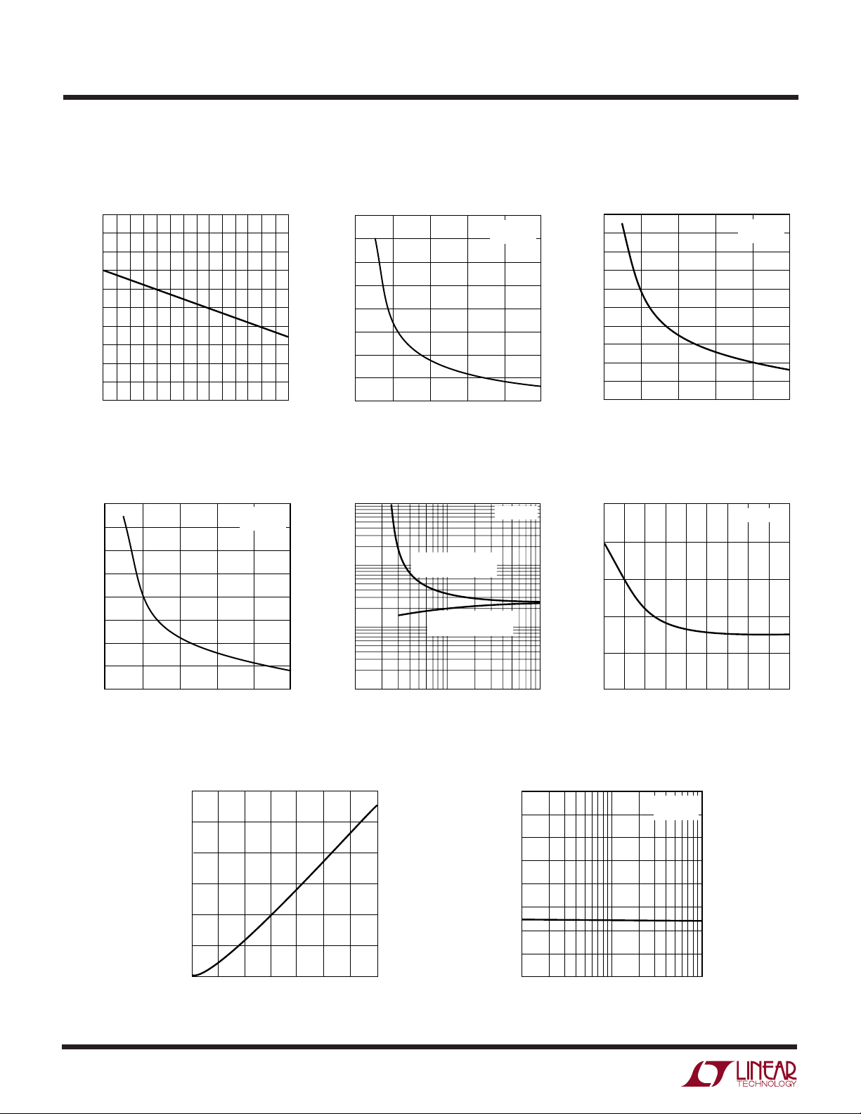
TYPICAL PERFOR A CE CHARACTERISTICS
Supply Current vs Temperature
20
18
16
(mA)
14
CC
12
10
8
6
SUPPLY CURRENT, I
4
2
0
–50 – 25 0
AMBIENT TEMPERATURE, TA (°C)
25
50 75 100 125
Total Error vs Reference Voltage
4
3
2
TOTAL ERROR (LSB)
1
1099 G01
TA = 25°C
T
= 2.5µs
C
VOS Error vs Reference Voltage
4
3
2
ERROR (LSB)
OS
V
1
0
0
13
REFERENCE VOLTAGE, V
2
Conversion Time vs R
100
10
1.0
CONVERSION TIME (µs)
RESISTOR BETWEEN
PIN 19 AND V
CC
RESISTOR BETWEEN
PIN 19 AND GND
EXT
TA = 25°C
T
C
(V)
REF
TA = 25°C
= 2.5µs
4
1099 G02
Linearity Error vs Reference
Voltage
1.0
0.9
0.8
0.7
0.6
0.5
0.4
0.3
LINEARITY ERROR (LBS)
0.2
0.1
0
5
0
Accuracy vs Conversion Time
1.0
0.8
0.6
0.4
0.2
TOTAL UNADJUSTED ERROR (LBS)
1
REFERENCE VOLTAGE, V
3
2
TA = 25°C
= 2.5µs
T
C
4
(V)
REF
TA = 25°C
5
1099 G03
4
0
0
REFERENCE VOLTAGE, V
REF
4
(V)
1099 G04
13
2
Conversion Time vs Temperature
1.8
1.6
1.4
1.2
1.0
0.8
CONVERSION TIME/CONVERSION TIME AT 25°C
0.6
–50
–25 0
AMBIENT TEMPERATURE, TA (°C)
25 75
5
50 100 125
0.1
10
1099 G07
RESISTANCE (kΩ)
4.5
4.0
CONVERSION TIME (µs)
3.5
3.0
2.5
2.0
1.5
100 1000
1099 G05
Signal-to-Noise Ratio (SNR) vs
Input Frequency
–36
–38
–40
–42
–44
–46
–48
SIGNAL-TO-NOISE RATIO, SNR (dB)
–50
–52
1
0
1.7 1.9
1.6
1.8
CONVERSION TIME (µs)
INPUT FREQUENCY (kHz)
10 100
2.0
TA = 25°C
= 2.5µs
T
C
1099 G08
2.3
2.1 2.5
2.2
2.4
1099 G06
UUU
PIN FUNCTIONS
LTC1099
VIN (Pin 1): Analog Input.
DB0 to DB3 (Pins 2 to 5): Data Outputs. DB0 = LSB.
WR/RDY (Pin 6): WR/RDY is an input when M0DE = VCC.
Falling edge of WR switches internal S/H to hold then
starts conversion. WR/RDY is an open drain output (active
pull-down) when M0DE = GND. RDY goes low at start of
conversion and pull-down is turned off when conversion
is complete. Resistive pull-up is usually used in this mode.
MODE (Pin 7): WR-RD when MODE = VCC. RD when
M0DE = GND. No internal pull-down.
RD (Pin 8): A Low on RD with CS Low Activates ThreeState Outputs. With MODE = GND and CS low, the falling
edge of RD switches internal S/H to hold and starts
conversion.
TEST CIRCUITS
t
1H
tr = 20ns, CL = 10pF
INT (Pin 9): Output that goes low when the conversion in
process is complete and goes high after data is read.
GND (Pin 10): Ground Connection.
REF– (Pin 11): Low Reference Potential (Analog Ground).
REF+ (Pin 12): High Reference Potential. V
= Full Scale
REF
= (REF+) – (REF–).
CS (Pin 13): Chip Select. When high, data outputs are high
impedance and all inputs are ignored.
DB4 to DB7 (Pins 14 to 17): Data Outputs. DB7 = MSB.
OFL (Pin 18): Overflow Output. Goes low when VIN > V
REF
.
TC (Pin 19): User Adjustable Conversion Time.
VCC (Pin 20): Positive Supply. 4.75V ≤ V
≤ 5.25V.
CC
RD
CS
RD
CS
t
r
V
V
CC
DATA
OUT
C
1k
L
t
0H
tr = 20ns, CL = 10pF
V
CC
V
CC
1k
DATA
OUT
C
L
DATA OUT
DATA OUT
RD
RD
GND
V
GND
V
GND
V
V
CC
10%
0H
CC
10%
CC
0L
t
50%
r
90%
50%
t
1H
90%
t
90%
0H
10%
1099 F01
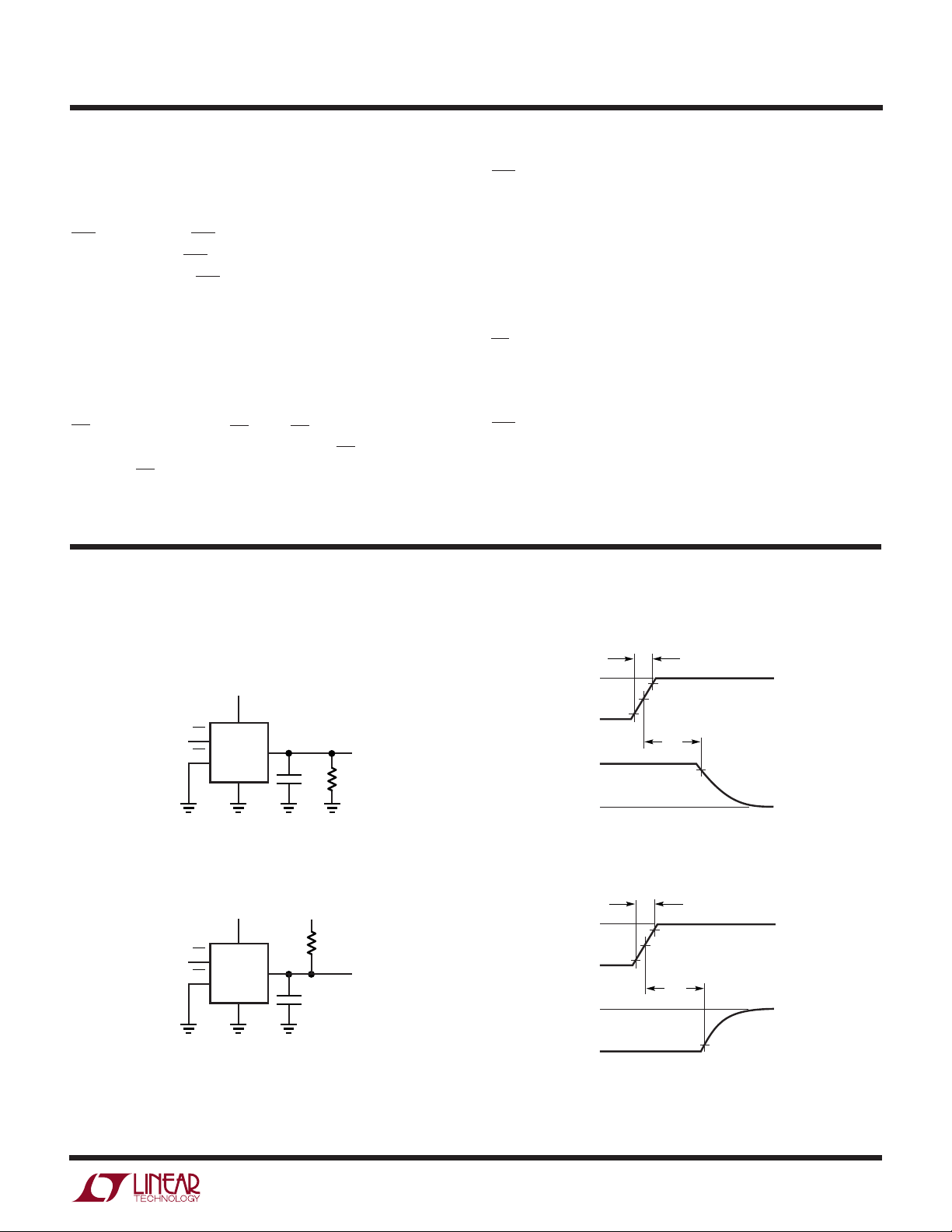
Figure 1. Three-State Test Circuit
5

LTC1099
UW
W
TI I G DIAGRA S
WR/RDY
DB0-DB7
CS
INT
CS
RD
t
RDY
t
CRD
t
ACC0
OLD DATA
t
ACC2
Figure 2. RD Mode (Pin 7 Is GND)
CS
t
P
NEW DATA
t
INTH
t1H, t
0H
1099 F02
WR/RDY
t
CWR
RD
INT
DB0-DB7
t
ACC2
Figure 3a. WR-RD Mode (Pin 7 Is HIGH and tRD > t
CS (GND)
RD (GND)
WR/RDY
INT
t
P
t1H, t
WR/RDY
t
CWR
RD
t
INTH
INT
t
0H
DB0-DB7
1099 F03A
)
CWR
t
IHWR
t
CWR
Figure 3b. WR-RD Mode (Pin 7 Is HIGH and tRD< t
t
P
ACC2
t
OLD DATA
ACC0
t
P
t
t1H, t
NEW DATA
INTH
0H
CWR
1099 F03B
)
6
DB0-DB7
OLD DATA
t
ACC0
NEW DATA
Figure 4. WR-RD Mode (Pin 7 Is HIGH) Standalone Operation
1099 F04

LTC1099
UU
U
FUNCTIONAL DESCRIPTIO
Figure 5 shows the functional block diagram for the
LTC1099 2-step flash ADC. It consists of two 4-bit flash
converters, a 4-bit DAC and a differencing circuit. The
conversion process proceeds as follows:
1. At the start of the conversion, the on-board sampleand-hold switches from the sample to the hold mode.
This is a true sample-and-hold with an acquisition time
of 240ns, an aperture time of 110ns and a tracking rate
of 2.5V/µs.
2. The held input voltage is converted by the 4-bit MSFlash ADC. This generates the upper or most significant
4-bits of the 8-bit output.
3. A 4-bit approximation, from the DAC output, is subtracted from the held input voltage.
4. The LS-Flash ADC converts the difference between the
held input voltage and the DAC approximation. This
generates the lower or least significant (LS) 4-bits of
the 8-bit output. The LS-Flash reference is one sixteenth of the MS-Flash reference. This effectively multiplies the difference by 16.
5. Upon the completion of the LS 4-bit flash the eight
output latches are updated simultaneously. At the same
time, the sample-and-hold is switched from the hold
mode to the acquire mode in preparation for the next
conversion.
The advantage of this approach is the reduction in the
amount of hardware required. A full flash converter requires 255 comparators while this approach requires only
31. The price paid for this reduction in hardware is an
increase in conversion time. A full flash converter requires
only one comparison cycle while this approach requires
two comparison cycles, hence 2-step flash.
This architecture is further simplified in the LTC1099 by
reusing the MS-Flash hardware to do the LS-Flash. This
reduces the number of comparators from 31 to 16. This is
possible because the MS and LS conversions are done at
different times.
To take the simple block diagram of Figure 5 and reconfigure
it to reuse the MS-Flash to do the LS-Flash is conceptually
simple, but from a hardware point of view is not practical.
A new six input switched capacitor comparator is used to
V
REF
B7
V
IN
+
–
∑
REMAINDER
Figure 5. 8-Bit 2-Step Semiflash A/D
MS
4-BIT
FLASH
V
REF
LS
4-BIT
FLASH
4-BIT
DAC
/16
B6
B5
B4
B3
B2
B1
B0
1099 F05
accomplish this function in a simple, although not straight
forward,␣ manner.
Figure 6 shows the six input switched capacitor comparator. Intuitively, the comparator is easy to understand by
noting that the common connection between the two input
capacitors, C1 and C2, acts like a virtual ground. In
operational amplifier circuits, current is summed at the
virtual ground node. Input voltage is converted to current
by the input resistors. In the switched capacitor comparator, input voltage is converted to charge by the input
capacitors and these charges are summed at the virtual
ground node.
A major advantage of this technique is that the switch-on
impedance has no affect on accuracy as long as sufficient
time exists to fully charge and discharge the capacitors.
During the first time period the T+ and TZ switches are
closed. This forces the common node between C1 and C2
to an arbitrary bias voltage. Since the capacitors subtract
out this voltage, it may be considered, for the sake of this
discussion, to be exactly zero (i.e., virtual ground). Note
7

LTC1099
UU
FUNCTIONAL DESCRIPTIO
T+
(+)
V
IN
(–)
MS TAP
(–)
DAC
(+)
0.5 LSB
(–)
0V
(–)
LS TAP
T
SAMPLE SAMPLE
Z
T+
T
U
–1
T
–2
T
Z
C1
VIRTUAL
GROUND
C2
C1 = C2
HOLD
T
Z
T
–1
T
–2
STROBE
Figure 6. Six Input Switched Capacitor Comparator
also that variations in the bias voltage with time and
temperature will also be rejected. In this state, C1 charges
to VIN. When TZ opens, VIN is held on C1.
The next step is the first comparison — the MS-Flash. T
Z
and T+ are opened and T–1 is closed. The equation for each
comparator is:
VIN + 0.5LSB – MS
TAP
= 0V
There are 16 identical comparators each tied to the tap on
a 16 resistor ladder. The MS tap voltages vary from V
to 0V in 16 equal steps of V
REF
/16.
REF
Notice that capacitor C2 adds 0.5LSB to VIN. This offsets
the converter transfer function by 0.5LSB, equally distributing the 1LSB quantization error to ±0.5LSB.
The outputs of the 16 comparators are temporarily latched
and drive the 4-bit DAC directly without need of decoding.
1099 F06
This holds the DAC output constant for the next step — the
LS conversion. The LS conversion is started when T–1 is
opened and T–2 is closed. Capacitor C1 subtracts the 4-bit
DAC approximation from VIN and inputs the difference
charge to the virtual ground node. The equation for each
comparator is:
VIN + 0.5LSB – V
DAC
– LS
TAP
= 0V
The 4-bit DAC approximation is input to all 16 comparators. The LS tap voltages are converted to charge by
capacitor C2. LS taps vary from V
steps of V
/256. The comparators look at the net charge
REF
/16V to 0V in 16 equal
REF
on the virtual ground node to perform the LS-Flash conversion. When this conversion is complete, the four LSBs
along with the four MSBs are transferred to the output
latches. In this way, all eight outputs will change
simultaneously.
8

DIGITAL I
1
2
20
19
5V
10k
1099 F07
LTC1099
U
TERFACE
The digital interface to the LTC1099 entails either controlling the conversion timing or reading data. There are two
basic modes for controlling and reading the A/D — the
Write-Read(WR-RD) mode and the Read (RD) mode.
WR-RD Mode (Pin 7 = High)
In the WR-RD mode, a conversion sequence starts on the
falling edge of WR with CS low (Figures 3a and 3b). This
is an edge-sensitive control function. The width of the WR
input is not important. All timing functions are internal to
the A/D.
The first thing to happen after the falling edge of WR is the
internal S/H is switched to hold. This typically takes 110ns
after WR falls and is the aperture time of the S/H.
Next, the A/D conversion takes place. The conversion time
is internally set at 2.5µs, but is user adjustable (see
Adjusting the Conversion Time). The end of conversion is
signaled by the high to low transition of INT. The S/H is
switched back to the acquire state as soon as the conversion is complete.
After the conversion is complete, the 8-bit result is available on the three-state outputs. The outputs are active with
RD and CS low. Output data is latched and, if no new
conversion is initiated, is available indefinitely as long as
the power is not turned off.
The WR-RD mode is also used for stand-alone operation.
By tying CS and RD low the data outputs will be continuously active (Figure 4). The falling edge of WR starts the
conversion sequence and when done new data will appear
on the outputs. All outputs will be updated simultaneously.
In stand-alone operation, the outputs will never be in a
high impedance state.
RD Mode (Pin 7 = Low)
In the RD mode, a conversion sequence is initiated by the
falling edge of RD when CS is low (Figure 2). The S/H is
switched to the hold state 110ns after the falling edge of
RD. It is switched back to the acquire state at the end of
conversion.
When RD goes low, with CS low, the result of the previous
conversion is output. This data stays there until the
ongoing conversion is complete (INT goes low). At this
time the outputs are updated with new data.
As long as CS and RD stay low long enough, the receiving
device will get the right data. Remember, the receiving
device reads data in on the rising edge of RD. The RDY
output facilitates making RD long enough.
In the RD mode, the WR input becomes the RDY output.
On the falling edge of RD, the RDY goes low. It is an open
drain output to allow a wired OR function so it requires a
pull-up resistor. At the end of conversion, the active pulldown is released and RDY goes high.
The RDY output is designed to interface to the Ready In
(RDYIN) function on many popular processors. RDYIN
allows these processors to work with slow memory by
stretching the RD strobe coming from the processor. RD
will remain low as long as RDY is low. In the case of the
LTC1099, RDY stays low until the conversion is complete
and new data is available on the outputs. This greatly
simplifies the programmers task. Each time data is required from the A/D a simple read is executed. The
hardware interface makes sure the RD strobe is long
enough.
Adjusting the Conversion Time
The conversion time of the LTC1099 is internally set at
2.5µs. If desired, it can be adjusted by forcing a voltage on
Pin 19. With Pin 19 left open, the conversion time runs
2.5µs. A convenient way to force the voltage is with the
circuit shown in Figure 7. To preset the conversion time to
a fixed amount, a resistor may be tied from Pin 19 to V
or GND. Tying it to VCC slows down the conversion and
tying it to GND will speed it up (see Typical Performance
Characteristics).
Figure 7. Adjusting the Conversion Time
CC
9

LTC1099
UU
ANALOG INTERFACE
The inclusion of a high quality sample-and-hold (S/H)
simplifies the analog interface to the LTC1099. All of the
error terms normally associated with an S/H (hold step,
offset, gain and droop errors) are included in the error
specifications for the A/D. This makes it easy for the
designer since all the error terms need not be taken into
account individually.
S/H Timing
A falling edge on the RD or WR input switches the S/H from
acquire to hold and starts the conversion. The aperture
time is the delay from the falling edge to the actual instant
when the S/H switches to hold. It is typically 110ns.
As soon as a conversion is complete (2.5µs typ), the S/H
switches back to the sample mode. Even though the
acquisition time is only 240ns, a new conversion cannot
be started for (700ns typ) after a conversion is completed.
Analog Input
The input to the A/D looks like a 60pF capacitor in series
with 550Ω (Figure 8).
V
IN
Figure 8. Equivalent Input Circuit
550Ω
TO A/D
60pF
1099 F08
With this high input capacitance care must be taken when
driving the inputs from a source amplifier. When the input
switch closes, an instantaneous capacitive load is applied
to the amplifier output. This acts like an impulse into the
amplifier and if it has poor phase margin the resulting
ringing can cause a considerable loss of accuracy. If the
amplifier is too slow the resulting settling tail will also
cause a loss of accuracy. The amplifier should also have
low open circuit output impedance. The LT1006 is an
excellent amplifier in this regard. It also works with a single
supply which fits nicely with the LTC1099.
Reference Inputs
Sixteen equal valued resistors are internally connected
between REF+ and REF–. Each resistor is nominally 200Ω
giving a total resistance of 3.2k between the reference
terminals. When VIN equals REF+, the output code will be
all ones. When VIN equals REF–, the output code will be all
zeros.
Although it is most common to connect REF+ to a 5V
reference and REF– to ground, any voltages can be used.
The only restrictions are REF+ >REF– and REF+ and REF
–
must be within the supply rails. As the reference voltage is
reduced the A/D will eventually lose accuracy. Accuracy is
quite good for references down to 1V.
Even though the reference drives a resistive ladder, a lot of
capacitive switching is taking place internally. For this
reason, driving the reference has the same characteristics
as driving VIN. A fast low impedance source is necessary.
The reference has the additional problem of presenting a
DC load to the driving source. This requires the DC as well
as the AC source impedance to be low.
Good Grounding
As with any precise analog system care must be taken to
follow good grounding practices when using the LTC1099.
The most noise free environment is obtained by using a
ground plane with GND (Pin 10) and REF– (Pin 11) tied to
it. Bypass capacitors from REF+ (Pin 12) and VCC (Pin 20)
with short leads are also required to prevent spurious
switching noise from affecting the conversion accuracy.
If a ground plane is not practical, single point grounding
techniques should be used. Ground for the A/D should not
be mixed in with other noisy grounds.
10

UU
ANALOG INTERFACE
APPLICATIONS
LTC1099
Analog Multiplier
The schematic Figure 9 shows the LTC1099 configured
with a DAC to form a two quadrant analog multiplier. An
input waveform is applied to the LTC1099 where it is
digitized at a 300kHz rate. The digitized signal is fed to the
DAC in “flow-through” mode where another signal is input
to the DAC reference input. In this way, the two analog
signals are multiplied to produce a double sideband amplitude modulated output. Figure 10 shows a 3kHz sine wave
multiplied by a 100Hz triangle.
(V
) 0V TO 5V
IN1
ANALOG
INPUT
CS AND RD LOW
1
2
3
4
5
6
7
8
9
N/C
10
15V
IN
LTC1099
DB0
DB1
DB2
DB3
WR/RDY
MODE
RD
INT
GND
LT1019-5
IN
GND
DB7
DB6
DB5
DB4
REF
REF
OUT
TRIM
20
19
18
17
16
15
14
13
CS
12
+
11
–
N/C
3MHz
OSC
5V
OUT
1
CLK
2
74LS90
3
4
N/C
5V
5
6
7
= ANALOG GROUND
= DIGITAL GROUND
14
13
12
11
10
9
8
÷ 10 = 300kHz
Note that since this is only a two quadrant multiplier, a
carrier component (the input to the LTC1099) will appear
in the output spectrum. Figure 11 shows the frequency
spectrum of a 42.5kHz sine wave multiplied by a 5kHz sine
wave. The depth of modulation is about 30dB. Figure 12
shows a 42.375kHz sine wave multiplied by a 30.875kHz
sine wave. Note that at these higher frequencies, the depth
of modulation is still about 30dB. The carrier feed-through
is seen in Figure 12.
) +10V TO –10V
(V
IN2
4
DB0-DB3
25k
5V
10µF
ANALOG
INPUT
MICROLINEAR
88
4
DB4-DB7
4.7µF
0.01µF
5V
REF
MP1208 DAC
1
CS
2
WR1
3
GND
4
DI5
5
DI4
6
DI3
7
DI2
8
DI1
9
DI0
10
V
11
RFB
12
REF
V
BYTE 1/
BYTE 2
WR2
XFER
DI6
DI7
DI8
DI9
DI10
DI11
I
OUT2
I
OUT1
CC
24
23
22
21
20
19
18
17
16
15
14
13
10pF
12V
1
+
LT1056
–
10µF
50k
OFFSET NULL
15V
5
–15V
15V
AGND
Figure 9
Figure 10
V
≅ 0V TO 5V
IN1
TRIANGLE INTO LTC1099
~100Hz
≅ ±4.8V SINE
V
IN2
INTO DAC ~ 3kHz
1099 F10
11

LTC1099
UU
ANALOG INTERFACE
10dBV/DIV
–70
0
32.5 34.5 36.5 38.5 40.5 42.5 44.5 46.5 48.5 50.5 52.5
37500Hz 42500Hz 47500Hz
Figure 11. Two Quadrant Multiplier Output Spectrum with 0V to
4.5V at 42.5kHz into LTC1099 and ±2V at 5kHz into DAC
0
10dBV/DIV
–70
5 152535455565758595105
30875Hz11500Hz 42375Hz 73250Hz
Figure 12. Two Quadrant Multiplier Output Spectrum with 0V to
4.5V at 42.375kHz into LTC1099 and ±2V at 30.875kHz into DAC
1099 F11
1099 F12
12

U
TYPICAL APPLICATIONS
LTC1099
TMS320C25 Interface Using RD Mode
5V
(B1, K11, L2)
V
SS
TMS320C25
READY
(B8) (C10) (H10)
(6)
MSC
(4)
(5)
1/2 74AS00
V
(3)
(A10, B11, H2, L6)
STRB
(K1)
A0
(K2)
A1
(L3)
A2
(J11)
IS
(K3)
A3
(D1)
D4
(C2)
D5
(C1)
D6
(B2)
D7
(F1)
D0
(E2)
D1
(E1)
D2
(D2)
D3
(1)
(2)
CC
74AS138
LTC1099
OFL
DB7
DB6
DB5
DB4
REF
REF
V
CC
Y0
Y1
Y2
Y3
Y4
Y5
Y6
V
CC
TC
CS
+
C1 C2
+
–
+
C1 C2
5V
1099 TA03
A
B
C
G2A
G2B
G1
5V
Y7
GND
ANALOG
INPUT
VOLTAGE
10k
5V
V
IN
DB0
DB1
DB2
DB3
WR/RDY
MODE
RD
INT
GND
C1 = 4.7µF TANTALUM
C2 = 0.1µF CERAMIC
TMS320C25 Assembly Code for RD Mode Interface to LTC1099
0001 0000
0002 0032 AORG >32
0003 0032 CE01 DINT Disable Interrupts
0004 0033 C800 LDPK >00 Data Page Pointer Is 0
0005 0034 8064 LOOP IN 100,PAO Input 1099 Data to Address 100
0006 0035 CB13 RPTK 12 Repeat Next Instruction 12 Times
0007 0036 5500 NOP Don’t Convert Again Too Soon
0008 0037 FF80 B LOOP Go for Another Conversion
13

LTC1099
U
TYPICAL APPLICATIONS
TMS320C25 Interface Using WR/RD Mode
5V
READY
(B8)
V
SS
TMS320C25
MSC
(C10)
R/W
V
CC
(A10, B11, H2, L6)
(K1)
A0
(K2)
A1
(L3)
A2
(J11)
IS
(K3)
A3
(F1)
D0
(E2)
D1
(E1)
D2
(D2)
D3
STRB
(H10)(H11)
5V
ANALOG
INPUT
VOLTAGE
5V
74F138
A
B
C
G2A
G2B
G1
Y7
GND
LTC1099
V
IN
DB0
DB1
DB2
DB3
WR/RDY
MODE
RD
INT
GND
DB7
DB6
DB5
DB4
REF
REF
V
V
OFL
CC
Y0
Y1
Y2
Y3
Y4
Y5
Y6
CC
T
CS
+
C
+
–
C3 C4
D7(B2)
D6(C1)
D5(C2)
D4(D1)
+
5V
5V
C1 C2
C5
0.1µF
+
C7
C6
74F00
IN1
IN1
OUT1
IN2
1N2
OUT2
GND
V
IN4
IN4
OUT4
IN3
IN3
OUT3
CC
C1, C3, C6 = 4.7µF TANTALUM
C2, C4, C5, C7, C8 = 0.1µF CERAMIC
5V
C8
0.1µF
TMS320C25 Assembly Code for WR/RD Mode Interface to
LTC1099
0001 0032 AORG >32
0002 0032 CE01 DINT Disable Interrupts
0003 0033 C800 LDPK >0 Data Page Pointer Is 0
0004 0034 E064 LOOP OUT >64.PAO Start LTC1099 Conversion
0005 0035 CB20 RPTK >12 Wait for Conversion to Finish
0006 0036 5500 NOP
0007 0037 8064 IN >64.PAO Read LTC1099 Data; Store in >64
0008 0038 FF80 B LOOP Do Again
1099 TA04
14

PACKAGE DESCRIPTIO
U
Dimensions in inches (millimeters) unless otherwise noted.
N Package
20-Lead PDIP (Narrow 0.300)
(LTC DWG # 05-08-1510)
1.040*
(26.416)
MAX
0.255 ± 0.015*
(6.477 ± 0.381)
19 1112
20
18
1517
131416
LTC1099
1234
0.300 – 0.325
(7.620 – 8.255)
0.009 – 0.015
(0.229 – 0.381)
+0.035
0.325
–0.015
+0.889
8.255
()
–0.381
*THESE DIMENSIONS DO NOT INCLUDE MOLD FLASH OR PROTRUSIONS.
MOLD FLASH OR PROTRUSIONS SHALL NOT EXCEED 0.010 INCH (0.254mm)
0.020
(0.508)
MIN
0.130 ± 0.005
(3.302 ± 0.127)
0.125
(3.175)
MIN
0.005
(0.127)
MIN
SW Package
20-Lead Plastic Small Outline (Wide 0.300)
(LTC DWG # 05-08-1620)
20
NOTE 1
0.100
(2.54)
19 18
BSC
5
0.045 – 0.065
(1.143 – 1.651)
0.496 – 0.512*
(12.598 – 13.005)
16
17
7
14 13
8
910
0.018 ± 0.003
(0.457 ± 0.076)
1112
0.394 – 0.419
(10.007 – 10.643)
0.065
(1.651)
TYP
N20 1098
6
15
0.291 – 0.299**
(7.391 – 7.595)
° – 8° TYP
0
0.093 – 0.104
(2.362 – 2.642)
0.010 – 0.029
(0.254 – 0.737)
0.009 – 0.013
(0.229 – 0.330)
NOTE:
1. PIN 1 IDENT, NOTCH ON TOP AND CAVITIES ON THE BOTTOM OF PACKAGES ARE THE MANUFACTURING OPTIONS.
THE PART MAY BE SUPPLIED WITH OR WITHOUT ANY OF THE OPTIONS
DIMENSION DOES NOT INCLUDE MOLD FLASH. MOLD FLASH SHALL NOT EXCEED 0.006" (0.152mm) PER SIDE
*
DIMENSION DOES NOT INCLUDE INTERLEAD FLASH. INTERLEAD FLASH SHALL NOT EXCEED 0.010" (0.254mm) PER SIDE
**
NOTE 1
× 45°
0.016 – 0.050
(0.406 – 1.270)
Information furnished by Linear Technology Corporation is believed to be accurate and reliable.
However, no responsibility is assumed for its use. Linear Technology Corporation makes no representation that the interconnection of its circuits as described herein will not infringe on existing patent rights.
0.050
(1.270)
BSC
2345
1
0.014 – 0.019
(0.356 – 0.482)
TYP
6
78
910
0.037 – 0.045
(0.940 – 1.143)
0.004 – 0.012
(0.102 – 0.305)
S20 (WIDE) 1098
15

LTC1099
TYPICAL APPLICATIO S
U
Cascading for 9-Bit Resolution
µP
BUS
CS
WR
RD
B0
B1
B2
B3
B4
B5
B6
B7
B8
OFL
13
8
6
2
3
4
5
14
15
16
17
18
13
8
6
2
3
4
5
14
15
16
17
18
CS
WR/RDY
RD
DB0
DB1
DB2
DB3
DB4
DB5
DB6
DB7
OFL
CS
WR/RDY
RD
DB0
DB1
DB2
DB3
DB4
DB5
DB6
DB7
OFL
LTC1099
LTC1099
V
V
MODE
V
REF
V
REF
GND
V
V
MODE
V
REF
V
REF
GND
20
5V
CC
1
IN
7
5V
12
+
11
–
1k
10
5k
20
5V
CC
1
IN
7
5V
12
+
11
–
10
1k
1099 TA02
4.7µF
V
IN
5V
4.7µF
4.7µF
RELATED PARTS
PART NUMBER DESCRIPTION COMMENTS
LTC1274/LTC1277 12-Bit, 100ksps Parallel/2-Byte ADC 5V or ± 5V, 10mW with 1µA Shutdown
LTC1279 12-Bit, 600ksps Parallel ADC 5V, 60mW, 70dB SINAD
LTC1406 8-Bit, 20Msps Parallel ADC 5V, 150mW, 48.5dB SINAD
LTC1409 12-Bit, 800ksps Parallel ADC ±5V, 80mW, 72.5dB SINAD
LTC1419 14-Bit, 800ksps Parallel ADC ±5V, 150mW, 81.5dB SINAD
sn1099 1099fas LT/TP 1100 2K REV A • PRINTED IN USA
LINEAR TECHNOLOGY CORPORATION 1989
16
Linear Technology Corporation
1630 McCarthy Blvd., Milpitas, CA 95035-7417
(408) 432-1900 ● FAX: (408) 434-0507
●
www.linear-tech.com
 Loading...