

FEATURES
■
Lowpass Filter with No DC Error
■
Low Passband Noise
■
Operates DC to 20kHz
■
Operates On a Single 5V Supply or Up to ±8V
■
5th Order Filter
■
Maximally Flat Response
■
Internal or External Clock
■
Cascadable for Faster Rolloff
■
Buffer Available
U
APPLICATIO S
■
60Hz Lowpass Filters
■
Antialiasing Filter
■
Low Level Filtering
■
Rolling Off AC Signals from High DC Voltages
■
Digital Voltmeters
■
Scales
■
Strain Gauges
LTC1062
5th Order Lowpass Filter
U
DESCRIPTIO
®
The LTC
lowpass filter with no DC error. Its unusual architecture
puts the filter outside the DC path so DC offset and low
frequency noise problems are eliminated. This makes the
LTC1062 very useful for lowpass filters where DC accuracy
is important.
The filter input and output are simultaneously taken across
an external resistor. The LTC1062 is coupled to the signal
through an external capacitor. This RC reacts with the
internal switched capacitor network to form a 5th order
rolloff at the output.
The filter cutoff frequency is set by an internal clock that
can be externally driven. The clock-to-cutoff frequency
ratio is typically 100:1, allowing the clock ripple to be
easily removed.
Two LTC1062s can be cascaded to form a 10th order quasi
max flat lowpass filter. The device can be operated with
single or dual supplies ranging from ±2.5V to ±9V.
1062 is a 5th order all pole maximally flat
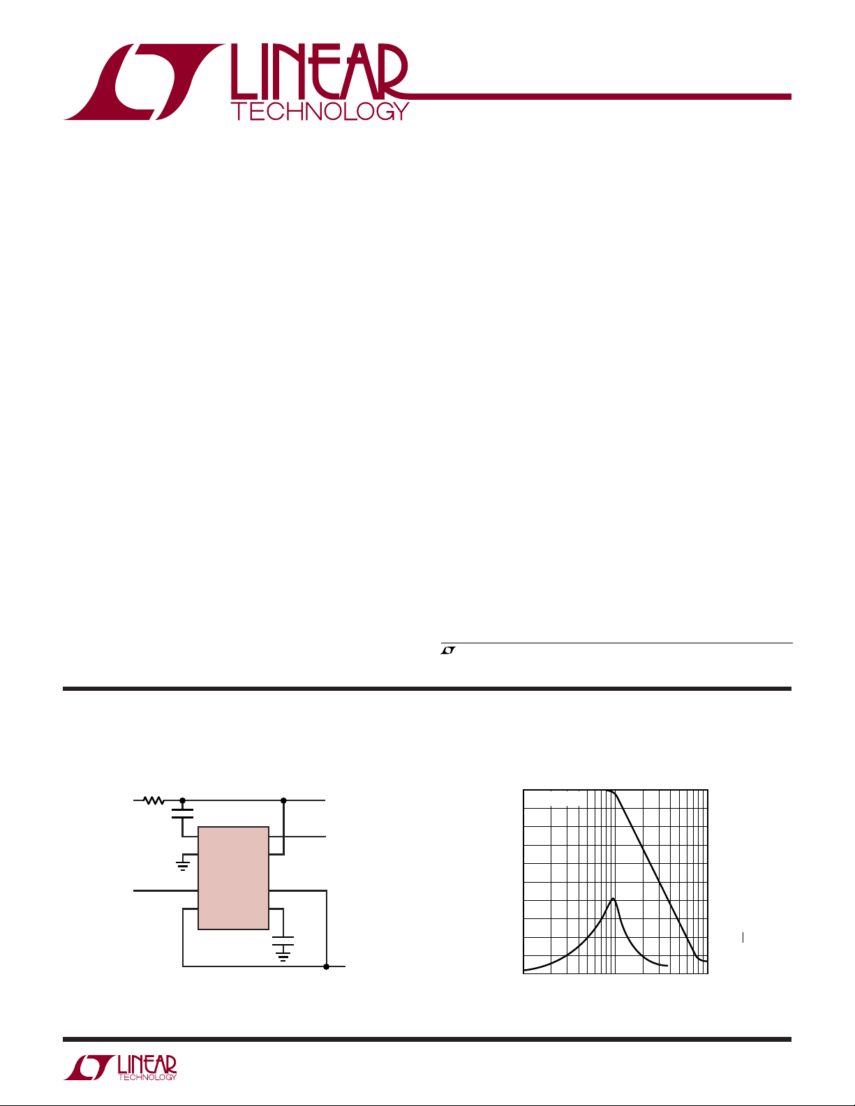
TYPICAL APPLICATIO
10Hz 5th Order Butterworth Lowpass Filter Filter Amplitude Response and Noise
25.8k
V
V
–
= –5V
IN
1µF
1
FB
2
AGND
3
V
4
DIVIDER
RATIO
NOTE: TO ADJUST OSCILLATOR FREQUENCY,
USE A 6800pF CAPACITOR IN SERIES
WITH A 50k POT FROM PIN 5 TO GROUND
LTC 1062
–
B
C
OUT
OUT
OSC
+
V
The LTC1062 is manufactured using Linear Technology’s
enhanced LTCMOS
, LTC and LT are registered trademarks of Linear Technology Corporation.
LTCMOS is a trademark of Linear Technology Corporation.
TM
silicon gate process.
U
DC ACCURATE
OUTPUT
8
7
6
5
C
OSC=
3900pF
BUFFERED
OUTPUT
1062 TA01
+
= 5V
V
0
C
= 3900pF
OSC
–10
–20
–30
–40
–50
–60
–70
AMPLITUDE RESPONSE (dB)
–80
–90
–100
1
INPUT FREQUENCY (Hz)
10 100
1062 TA02
FILTER OUTPUT NOISE (µV/√Hz)
50
40
30
20
10
0
1062fd
1
LTC1062
WWWU
ABSOLUTE AXI U RATI GS
(Note 1)
Total Supply Voltage (V+ to V–) ............................... 18V
–
Input Voltage at Any Pin ..... V
– 0.3V ≤ VIN ≤ V+ + 0.3V
Operating Temperature Range
LTC1062M (OBSOLETE)............. –55°C ≤ T
LTC1062C ................................... – 40°C ≤ T
UU
W
≤ 125°C
A
≤ 85°C
A
PACKAGE/ORDER I FOR ATIO
TOP VIEW
FB
1
AGND
2
–
V
3
DIVIDER
4
RATIO
N8 PACKAGE
8-LEAD PDIP
T
= 100°C, θ
J MAX
J8 PACKAGE 8-LEAD CERDIP
T
= 150°C, θ
J MAX
Consider the N8 Package as an Alternate Source
B
8
OUT
OUT
7
+
V
6
C
5
OSC
= 130°C/W
JA
= 100°C/W
JA
OBSOLETE PACKAGE
ORDER PART
NUMBER
LTC1062CN8
LTC1062MJ8
LTC1062CJ8
Storage Temperature Range ................. –65°C to 150°C
Lead Temperature (Soldering, 10 sec)................. 300°C
ORDER PART
NUMBER
LTC1062CSW
NC
NC
AGND
DIVIDER
RATIO
NC
NC
1
2
3
FB
4
5
V–
6
7
8
SW PACKAGE
16-LEAD PLASTIC SO
T
= 150°C, θ
J MAX
TOP VIEW
JA
= 90°C/W
16
NC
15
NC
14
B
OUT
13
OUT
+
12
V
11
C
OSC
10
NC
9
NC
Consult LTC Marketing for parts specified with wider operating temperature ranges.
ELECTRICAL CHARACTERISTICS
The
● denotes specifications which apply over the full operating tempera-
ture range, otherwise specifications are at TA = 25°C. V+ = 5V, V– = – 5V, unless otherwise specified. AC output measured at Pin 7,
Figure 1.
PARAMETER CONDITIONS MIN TYP MAX UNITS
Power Supply Current C
Input Frequency Range 0 to 20 kHz
Filter Gain at fIN = 0 f
= 0.5fC (Note 2) C = 0.01µF, R = 25.78k –0.02 –0.3 dB
f
IN
f
= f
IN
C
= 2f
f
IN
C
= 4f
f
IN
C
Clock-to-Cutoff Frequency Ratio, f
CLK/fC
Filter Gain at fIN = 16kHz f
f
Tempco f
CLK/fC
Filter Output (Pin 7, Pin 13 in SW16) DC Swing Pin 7/Pin13 (SW16) Buffered with an External Op Amp ● ±3.5 ±3.8 V
Clock Feedthrough 1mV
(Pin 5 to V–, Pin 11 in SW16) = 100pF 4.5 7 mA
OSC
= 100kHz, Pin 4 (Pin 6 in SW16) at V+, 0.00 dB
CLK
f
= 100kHz, Pin 4 (Pin 6 in SW16) at V+,100 ±1%
CLK
● 10 mA
● –2 –3.00 dB
● –28–30.00 dB
● –52–60.00 dB
C = 0.01µF, R = 25.78k
= 400kHz, Pin 4 at V+, C = 0.01µF, R = 6.5k ● –43 –52 dB
CLK
= 400kHz, Pin 4 at V+, C = 0.01µF, R = 6.5k 10 ppm/°C
CLK
P-P
2
1062fd
LTC1062
ELECTRICAL CHARACTERISTICS
The ● denotes specifications which apply over the full operating tempera-
ture range, otherwise specifications are at TA = 25°C. V+ = 5V, V– = – 5V, unless otherwise specified, AC output measured at Pin 7,
Figure 1.
PARAMETER CONDITIONS MIN TYP MAX UNITS
Internal Buffer
Bias Current 250 pA
● 170 1000 pA
Offset Voltage 220 mV
Voltage Swing R
Short-Circuit Current Source/Sink 40/3 mA
Clock (Note 3)
Internal Oscillator Frequency C
Max Clock Frequency 4 MHz
Pin 5 (Pin 11 in SW16) Source or Sink Current ● 40 80 µA
Note 1: Absolute Maximum Ratings are those values beyond which the life of
a device may be impaired.
Note 2: f
is the frequency where the gain is –3dB with respect to the input
C
signal.
= 20k ● ±3.5 ±3.8 V
LOAD
(Pin 5 to V–, Pin 11 in SW16) = 100pF 25 32 50 kHz
OSC
● 15 65 kHz
Note 3: The external or driven clock frequency is divided by either 1, 2 or 4
depending upon the voltage at Pin 4. For the N8 package, when Pin 4 = V
ratio = 1; when Pin 4 = GND, ratio = 2; when Pin 4 = V
–
, ratio = 4.
+
,
UW
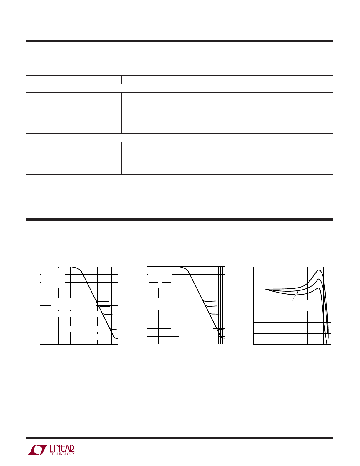
TYPICAL PERFOR A CE CHARACTERISTICS
Amplitude Response Normalized
to the Cutoff Frequency
0
= ±2.5V
V
S
= 25°C
T
–10
A
f
1
C
0.1
2πRC
=
1.62
f
CLK
f
CLK
= 500kHz, fC = 5kHz
= 250kHz, fC = 2.5kHz
f
= 100kHz, fC = 1kHz
CLK
f
= 10kHz, fC = 100Hz
CLK
f
= 1kHz, fC = 10Hz
CLK
110
fIN/f
C
–20
–30
–40
–50
–60
RESPONSE (dB)
–70
–80
–90
–100
1062 G01
Amplitude Response Normalized
to the Cutoff Frequency
0
V
= ±2.5V
S
= 25°C
T
–10
A
f
1
C
0.1
2πRC
f
=
f
CLK
1.62
CLK
= 500kHz, fC = 5kHz
= 250kHz, fC = 2.5kHz
f
= 100kHz, fC = 1kHz
CLK
f
= 10kHz, fC = 100Hz
CLK
f
= 1kHz, fC = 10Hz
CLK
110
fIN/f
C
–20
–30
–40
–50
–60
RESPONSE (dB)
–70
–80
–90
–100
1062 G01
Passband Gain
vs Input Frequency
0.4
VS = ±5V
= 25°C
T
A
0.2
= 100kHz
f
CLK
0
–0.2
–0.4
–0.6
PASSBAND GAIN (dB)
–0.8
–1.0
0.1 0.2 0.4 0.6 0.8
1
2πRC
=
2πRC
f
1.62
C
1
fIN/f
f
C
=
1.6
1
2πRC
C
f
C
=
1.64
1
1062 G03
1062fd
3
LTC1062
UW
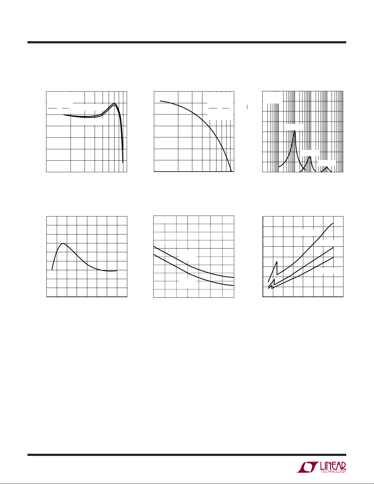
TYPICAL PERFOR A CE CHARACTERISTICS
Passband Gain
vs Input Frequency and Temperature
0.4
VS = ±5V
f
= 100kHz
CLK
0.2
0
–0.2
–0.4
–0.6
PASSBAND GAIN (dB)
–0.8
–1.0
0.1 0.2 0.4 0.6 0.8
1
2πRC
f
C
=
1.62
TA = 125°C
TA = –55°C
fIN/f
C
Normalized Oscillator Frequency,
f
vs Supply Voltage
OSC
1.6
1.5
1.4
1.3
1.2
AT 5V SUPPLY
1.1
OSC
1.0
TO f
0.9
0.8
OSCILLATOR FREQUENCY NORMALIZED
0.7
4
8
6
10
V
12
SUPPLY
14
(V)
Passband Phase Shift
vs Input Frequency Filter Noise Spectral Density
80
VS = ±5V
= 25°C
T
A
70
60
50
40
30
20
FILTER OUTPUT NOISE (µV/√Hz)
10
0
0.1 10 100 10k
fC = 10Hz
fC = 100Hz
fC = 1kHz
1
CUTOFF FREQUENCY (Hz)
Power Supply Current
vs Power Supply Voltage
16
14
12
10
8
6
SUPPLY CURRENT (mA)
4
2
0
6
4
8
POWER SUPPLY VOLTAGE (V)
10
TA = –55°C
12
14
TA = 125°C
16
1k
1062 G06
TA = 25°C
18
1062 G09
20
1062 G04
1
0
–30
–60
–90
–120
PHASE SHIFT (DEG)
–150
–180
–210
0.1 0.2 0.4 0.6 0.8
fIN/f
Oscillator Frequency, f
VS = ±5V
= 100kHz
f
CLK
f
1
C
=
1.62
2πRC
TA = 25°C
1
C
1062 G05
OSC
vs Ambient Temperature
260
C
= 0pF
OSC
240
220
200
180
160
140
120
100
OSCILLATOR FREQUENCY (kHz)
80
18
16
20
1062 G07
60
–50
–25
V+ = 10V
–
= 0V
V
V+ = 5V
–
= 0V
V
50
25
0
AMBIENT TEMPERATURE (°C)
75
100
125
1062 G08
4
1062fd

BLOCK DIAGRA
LTC1062
W
For Adjusting Oscillator Frequency, Insert a 50k Pot in Series with C
FB
1
AGND
2
–
V
3
4
÷
AC TEST CIRCUIT
V
R = 25.8k
IN
C = 0.01µF
50Ω
V
–
= –5V
1
2
3
4
FB
AGND
–
V
DIVIDER
RATIO
SWITCHED
CAPACITOR
NETWORK
f
CLK
CLOCK GEN
÷ 1, 2, 4 OSC
8
B
OUT
7
OUT
LTC1062
6
+
V
5
C
OSC
R′
1062 F01
–5V
. Use Two Times Calculated C
OSC
BY CONNECTING PIN 4 TO V+, AGND OR V–, THE
B
8
OUT
×1
5V
f
= 100kHz
CLK
5V
7
6
5
1062 BD
0.1µF
OUT
V
C
3
2
+
OSC
+
LTC1052
–
1
–5V
OUTPUT FREQUENCY OF THE INTERNAL CLOCK
GENERATOR IS THE OSCILLATOR FREQUENCY DIVIDED BY 1, 2, 4. THE (f
WITH RESPECT TO THE INTERNAL CLOCK GENERATOR OUTPUT FREQUENCY. PIN 5 CAN BE DRIVEN
WITH AN EXTERNAL CMOS LEVEL CLOCK. THE
LTC1062 CAN ALSO BE SELF-CLOCKED BY CONNECTING AN EXTERNAL CAPACITOR (C
GROUND (OR TO V
THIS CONDITION AND WITH ±5V SUPPLIES, THE
INTERNAL OSCILLATOR FREQUENCY IS:
f
≅ 140kHz [33pF/(33pF + C
OSC
5V
7
6
MEASURED
OUTPUT
8
4
0.1µF
CLK/fC
–
IF C
IS POLARIZED). UNDER
OSC
FOR BEST MAX FLAT APPROXIMATION,
THE INPUT RC SHOULD BE SUCH AS:
1
2πRC
A 0.5k RESISTOR, R′, SHOULD BE USED IF
THE BIPOLAR EXTERNAL CLOCK IS APPLIED
BEFORE THE POWER SUPPLIES TURN ON
) RATIO OF 100:1 IS
)]
OSC
f
CLK
=
100
OSC
) TO
OSC
1
•
1.63
Figure 1
1062fd
5

LTC1062
WUUU
APPLICATIO S I FOR ATIO
Filter Input Voltage Range
Every node of the LTC1062 typically swings within 1V of
either voltage supply, positive or negative. With the appropriate external (RC) values, the amplitude response of all
the internal or external nodes does not exceed a gain of
0dB with the exception of Pin 1. The amplitude response
of the feedback node (Pin 1) is shown in Figure 2. For an
input frequency around 0.8 • f
, the gain is 1.7V/V and, with
C
±5V supplies, the peak-to-peak input voltage should not
exceed 4.7V. If the input voltage goes beyond this value,
clipping and distortion of the output waveform occur, but
the filter will not get damaged nor will it oscillate. Also, the
absolute maximum input voltage should not exceed the
power supplies.
6
4
2
0
–2
(dB)
IN
–4
/V
–6
PIN1
V
–8
–10
–12
–14
0.1
Figure 2. Amplitude Response of Pin 1
110
fIN/f
VS = ±5V
f
1
C
=
1.62
2πRC
C
1062 F02
Internal Buffer
The internal buffer out (Pin 8) and Pin 1 are part of the
signal AC path. Excessive capacitive loading will cause
gain errors in the passband, especially around the cutoff
frequency. The internal buffer gain at DC is typically
0.006dB. The internal buffer output can be used as a filter
output, however, it has a few millivolts of DC offset. The
temperature coefficient of the internal buffer is typically
1µV/°C.
Filter Attenuation
The LTC1062 rolloff is typically 30dB/octave. When the
clock and the cutoff frequencies increase, the filter’s
maximum attenuation decreases. This is shown in the
Typical Performance Characteristics. The decrease of the
maximum attenuation is due to the rolloff at higher
frequencies of the loop gains of the various internal
feedback paths and not to the increase of the noise floor.
For instance, for a 100kHz clock and 1kHz cutoff frequency, the maximum attenuation is about 64dB. A 4kHz,
1V
at the output. A 6kHz, 1V
input signal will be predictably attenuated by 60dB
RMS
input signal will be attenu-
RMS
ated by 64dB and not by 77dB as an ideal 5th order
maximum flat filter would have dictated. The LTC1062
output at 6kHz will be about 630µV
RMS noise from DC to 17kHz was 100µV
. The measured
RMS
which is
RMS
16dB below the filter output.
C
, Pin 5
OSC
The C
C
OSC
, Pin 5, can be used with an external capacitor,
OSC
, connected from Pin 5 to ground. If C
is polarized
OSC
it should be connected from Pin 5 to the negative supply,
Pin 3. C
lowers the internal oscillator frequency. If
OSC
Pin 5 is floating, an internal 33pF capacitor plus the
external interpin capacitance set the oscillator frequency
around 140kHz with ±5V supply. An external C
OSC
will
bring the oscillator frequency down by the ratio (33pF)/
(33pF + C
). The Typical Performance Characteristics
OSC
curves provide the necessary information to get the internal oscillator frequency for various power supply ranges.
Pin 5 can also be driven with an external CMOS clock to
override the internal oscillator. Although standard 7400
series CMOS gates do not guarantee CMOS levels with the
current source and sink requirements of Pin 5, they will, in
reality, drive the C
pin. CMOS gates conforming to
OSC
standard B series output drive have the appropriate voltage levels and more than enough output current to
simultaneously drive several LTC1062 C
pins. The
OSC
typical trip levels of the internal Schmitt trigger which
input is Pin 5, are given in Table 1.
Table 1
V
SUPPLY
±2.5V 0.9V –1V
±5V 1.3V –2.1V
±6V 1.7V –2.5V
±7V 1.75V –2.9V
+
V
TH
–
V
TH
1062fd
6

WUUU
APPLICATIO S I FOR ATIO
LTC1062
Divide By 1, 2, 4 (Pin 4)
+
By connecting Pin 4 to V
, to mid supplies or to V–, the
clock frequency driving the internal switched capacitor
network is the oscillator frequency divided by 1, 2, 4
respectively. Note that the f
ratio of 100:1 is with
CLK/fC
respect to the internal clock generator output frequency.
The internal divider is useful for applications where octave
tuning is required. The ÷2 threshold is typically ±1V from
the mid supply voltage.
Transient Response
Figure 3 shows the LTC1062 response to a 1V input step.
200mV/VERT DIV
50ms/HORIZ DIV, f
5ms/HORIZ DIV, f
0.5ms/HORIZ DIV, f
f
1
C
=
1.62
2πRC
Filter Noise
The filter wideband RMS noise is typically 100µV
RMS
for
±5V supply and it is nearly independent from the value of
the cutoff frequency. For single 5V supply the RMS noise
is 80µV
the passband, that is from DC to f
. Sixty-two percent of the wideband noise is in
RMS
. The noise spectral
C
density, unlike conventional active filters, is nearly zero for
frequencies below 0.1 • f
. This is shown in the Typical
C
Performance Characteristics section. Table 2 shows the
LTC1062 RMS noise for different noise bandwidths.
f
1
= 10Hz
C
= 100Hz
C
= 1kHz
C
2πRC
C
=
1.94
Table 2
1
2πRC
Figure 3. Step Response to a 1V Peak Input Step
NOISE BW RMS NOISE (VS = ±5V)
DC – 0.1 • f
DC – 0.25 • f
DC – 0.5 • f
DC – 1 • f
DC – 2 • f
C
C
C
C
C
2µV
8µV
20µV
62µV
100µV
f
C
=
2.11
1062fd
7

LTC1062
TYPICAL APPLICATIO S
U
AC Coupling an External CMOS Clock Powered
from a Single Positive Supply, V
V
IN
C
1
FB
2
AGND
LTC1062
3
–
–
V
V
4
DIVIDER
RATIO
B
C
OUT
OUT
OSC
8
7
6
+
V
5
V
OUT
+
V
0.01µF
100k
1062 TA03
+
+
V
0
Adding an External (R1, C1) to Eliminate the Clock Feedthrough and
to Improve the High Frequency Attenuation Floor
–
C1
0.01C
EXTERNAL
BUFFER
+
V
OUT
R
V
IN
C
1
FB
2
AGND
3
–
V
V
4
DIVIDER
RATIO
LTC1062
–
B
OUT
C
OUT
OSC
+
V
R1
10R
8
7
6
5
1062 TA04
+
V
f
CLK
Filtering AC Signals from High DC Voltages
HIGH DC INPUT = 100V
–
= –5V
V
8
R
25.8k
V
IN
EXAMPLE:
= 100KHz, fC = 1kHz. THE FILTER ACCURATELY PASSES
f
CLK
THE HIGH DC INPUT AND ACTS AS 5TH ORDER LP FILTER
FOR THE AC SIGNALS RIDING ON THE DC
V+ = 5V
C
0.01µF
1
2
3
4
FB
AGND
LTC1062
–
V
DIVIDER
RATIO
B
C
OUT
OUT
V
OSC
+
1062 TA05
C
0.01µF
8
12R
309.6k
7
6
5
CLK IN = f
DC OUTPUT
• 100
C
Passband Amplitude Response for the
High DC Accurate 5th Order Filter
0.2
0
–0.2
–0.4
–0.6
–0.8
PASSBAND GAIN (dB)
–1.0
–1.2
VS = ±5V
= 100kHz
f
CLK
–1.4
0.01
0.1 1
fIN/f
C
1062 TA06
1062fd

TYPICAL APPLICATIO S
LTC1062
U
Cascading Two LTC1062s to Form a Very
Selective Clock Sweepable Bandpass Filter
R1
10k
V
IN
R2
10k
1
FB
2
AGND
LTC1062
3
4
–
V
DIVIDER
RATIO
–5V 5V
B
C
OUT
OUT
OSC
8
7
6
+
V
5
R′1
10k
R′2
12.5k
–5V
1
2
3
4
FB
AGND
LTC1062
–
V
DIVIDER
RATIO
B
C
OUT
OUT
V
OSC
8
V
OUT
7
6
+
5V
5
f
CLK
1062 TA07
Clock Tunable Notch Filter
For Simplicity Use R3 = R4 = R5 = 10k;
R5
= 1.234, =
R2
R1
V
IN
R2 R3
1
–5V
2
3
4
FB
AGND
V
DIVIDER
RATIO
LTC1062
–
B
C
OUT
OUT
V
OSC
f
CLK
f
NOTCH
8
7
6
+
5V
5
f
1062 TA08
CLK
79.3
1
R5R4
–
V
+
OUT
Frequency Response of the Bandpass Filter
–10
–20
–30
(dB)
–40
–50
–60
–70
–80
–90
20
10
0
0.5
1.5 2 2.5
1
VS = ±5V
R1
R2
R′1
R′2
VIN = 100mV
3 3.5 4 4.5
(kHz)
= 1
= 0.8
RMS
1062 TA09
Frequency Response of the Notch Filter
–10
0
10
20
30
(dB)
40
50
60
70
300 500 700 1100
100
(Hz)
900
1062 TA10
1062fd
9

LTC1062
TYPICAL APPLICATIO S
25.8k
V
IN
–5V
1µF
1
FB
2
AGND
LTC1062
3
–
V
4
DIVIDER
RATIO
10Hz, 10TH ORDER DC ACCURATE LOWPASS FILTER
60dB/OCTAVE ROLLOFF
0.5dB PASSBAND ERROR, 0dB DC GAIN
MAXIMUM ATTENUATION 110dB (f
U
B
C
OUT
OUT
OSC
Simple Cascading Technique
412k
0.1µF
8
7
6
+
V
5
–5V
100dB (f
95dB (f
CLK
1
2
3
4
CLK
CLK
FB
AGND
–
V
DIVIDER
RATIO
= 10kHz)
= 1kHz)
= 1MHz)
LTC1062
B
C
OUT
OUT
V
OSC
5V
3
8
7
6
+
5
0.1µF
1062 TA11
V
f
2
+
CLK
+
LTC1052
–
= 5V
= 1kHz
7
6
DC ACCURATE
OUTPUT
8
4
1
0.1µF
–5V
100Hz, 50Hz, 25Hz 5th Order DC Accurate LP Filter
25.8k
V
IN
(HIGH, GROUND, LOW)
CONTROL
0.1µF
1
FB
2
AGND
LTC1062
3
4
5V
100k
100k
–
V
DIVIDER
RATIO
100k
–5V 5V
0.1µF
1
13 5
2
1/2 CD4016
8
B
C
–5V
5V
100k
B
OUT
7
OUT
6
+
V
5
OSC
TO PIN 5 OF CD4016
BY CONNECTING PIN 4 OF THE LTC1062
HIGH/GROUND/LOW THE FILTER CUTOFF
FREQUENCY IS 100Hz/50Hz/25Hz
TO PIN 13 OF CD4016
OUT
10kHz
CLK IN
V
OUT
0.2µF
3
4
10
–5V
1062 TA12
1062fd

TYPICAL APPLICATIO S
7th Order 100Hz Lowpass Filter with Continuous Output Filtering, Output Buffering and Gain Adjustment
LTC1062
U
R3
2
–
C2
RMS
0.1µF
3
LTC1052
+
1
2.6k
V
IN
1µF
1
FB
2
AGND
3
–5V
V
4
5V
DIVIDER
RATIO
THE LTC1052 IS CONNECTED AS A 2ND ORDER SALLEN AND KEY LOWPASS FILTER WITH A CUTOFF
FREQUENCY EQUAL TO THE CUTOFF FREQUENCY OF THE LTC1062. THE ADDITIONAL FILTERING
ELIMINATES ANY 10kHz CLOCK FEEDTHROUGH PLUS DECREASES THE WIDEBAND NOISE OF THE FILTER
DC OUTPUT OFFSET (REFERRED TO A DC GAIN OF UNITY) = 5µV MAX
WIDEBAND NOISE (REFERRED TO A DC GAIN OF UNITY) = 60µV
OUTPUT FILTER COMPONENT VALUES
DC GAIN
R3
1
∞
10
3.57k
LTC1062
–
R4
0
32.4k
R1
B
OUT
OUT
C
OSC
R1
14.3k
46k
R2
C1
8
7
6
+
5V
V
5
10kHz
CLK IN
1062 TA13
R2
C1
53.6k
274k
0.1µF
0.01µF
C2
0.033µF
0.02µF
R4
5V
7
6
8
4
0.1µF
–5V
V
OUT
10µF
SOLID
TANTALUM
Single 5V Supply 5th Order LP Filter
R
V
IN
5V
25k
+
25k
FOR A 10Hz FILTER: R = 29.4k, C = 1µF, f
THE FILTER IS MAXIMALLY FLAT FOR
C C
1
FB
2
AGND
LTC1062
3
–
V
4
5V
DIVIDER
RATIO
12R
B
C
OUT
OUT
OSC
8
BUFFERED
OUTPUT
7
6
+
5V
V
5
CLK
2πRC
CLK
1
= 1kHz
f
C
=
1.84
DC ACCURATE
OUTPUT
1062 TA14
1062fd
11

LTC1062
TYPICAL APPLICATIO S
R
9.09k
V
IN
V
C
1µF
1
FB
2
AGND
LTC1062
3
–
–
V
4
DIVIDER
RATIO
U
A Lowpass Filter with a 60Hz Notch
R6
19.35k
B
C
OUT
OUT
OSC
R3
20k
R2
20k
8
7
6
+
V
+
V
5
CLK IN
2.84kHz
1
2πRC
f
CLK
=
100 • 1.62
R4
10k
–
A1
1/2 LT1013
+
R5
10k
C7
0.1µF
R7
20k
–
A2
1/2 LT1013
+
1062 TA15
V
OUT
Frequency Response of the Above Lowpass Filter
with the Notch f
–10
0
10
20
(Hz)
IN
30
/V
OUT
40
V
50
60
70
1
10 100 1k
fIN (Hz)
NOTCH
= f
CLK
/47.3
1062 TA16
12
1062fd

PACKAGE DESCRIPTIO
LTC1062
U
J8 Package
8-Lead CERDIP (Narrow .300 Inch, Hermetic)
(Reference LTC DWG # 05-08-1110)
CORNER LEADS OPTION
(4 PLCS)
.023 – .045
(0.584 – 1.143)
HALF LEAD
.045 – .068
(1.143 – 1.650)
FULL LEAD
OPTION
.300 BSC
(7.62 BSC)
.008 – .018
(0.203 – 0.457)
NOTE: LEAD DIMENSIONS APPLY TO SOLDER DIP/PLATE
OR TIN PLATE LEADS
0° – 15°
OPTION
OBSOLETE PACKAGE
.005
(0.127)
MIN
.025
(0.635)
RAD TYP
.045 – .065
(1.143 – 1.651)
.014 – .026
(0.360 – 0.660)
.405
(10.287)
MAX
87
12
65
3
4
.220 – .310
(5.588 – 7.874)
.015 – .060
(0.381 – 1.524)
.100
(2.54)
BSC
.200
(5.080)
MAX
.125
3.175
MIN
J8 0801
1062fd
13

LTC1062
PACKAGE DESCRIPTIO
U
N8 Package
8-Lead PDIP (Narrow .300 Inch)
(Reference LTC DWG # 05-08-1510)
.255 ± .015*
(6.477 ± 0.381)
.400*
(10.160)
MAX
87 6
5
12
.300 – .325
(7.620 – 8.255)
.065
(1.651)
.008 – .015
(0.203 – 0.381)
+.035
.325
–.015
+0.889
8.255
()
–0.381
NOTE:
1. DIMENSIONS ARE
*THESE DIMENSIONS DO NOT INCLUDE MOLD FLASH OR PROTRUSIONS.
MOLD FLASH OR PROTRUSIONS SHALL NOT EXCEED .010 INCH (0.254mm)
INCHES
MILLIMETERS
TYP
.045 – .065
(1.143 – 1.651)
.100
(2.54)
BSC
3
4
.130 ± .005
(3.302 ± 0.127)
.120
(3.048)
MIN
.018 ± .003
(0.457 ± 0.076)
.020
(0.508)
MIN
N8 1002
14
1062fd

PACKAGE DESCRIPTIO
.030 ±.005
TYP
N
U
SW Package
16-Lead Plastic Small Outline (Wide .300 Inch)
(Reference LTC DWG # 05-08-1620)
.050 BSC
.045 ±.005
16
N
.398 – .413
(10.109 – 10.490)
15 14
NOTE 4
13
LTC1062
12
10 9
11
.420
MIN
123 N/2
RECOMMENDED SOLDER PAD LAYOUT
.291 – .299
(7.391 – 7.595)
NOTE 4
.010 – .029
.005
(0.127)
RAD MIN
.009 – .013
(0.229 – 0.330)
NOTE:
1. DIMENSIONS IN
2. DRAWING NOT TO SCALE
3. PIN 1 IDENT, NOTCH ON TOP AND CAVITIES ON THE BOTTOM OF PACKAGES ARE THE MANUFACTURING OPTIONS.
THE PART MAY BE SUPPLIED WITH OR WITHOUT ANY OF THE OPTIONS
4. THESE DIMENSIONS DO NOT INCLUDE MOLD FLASH OR PROTRUSIONS.
MOLD FLASH OR PROTRUSIONS SHALL NOT EXCEED .006" (0.15mm)
(0.254 – 0.737)
NOTE 3
INCHES
(MILLIMETERS)
× 45°
.016 – .050
(0.406 – 1.270)
.325 ±.005
0° – 8° TYP
NOTE 3
.093 – .104
(2.362 – 2.642)
(1.270)
1
.050
BSC
.014 – .019
(0.356 – 0.482)
2345
TYP
6
.394 – .419
(10.007 – 10.643)
N/2
78
.037 – .045
(0.940 – 1.143)
.004 – .012
(0.102 – 0.305)
S16 (WIDE) 0502
Information furnished by Linear Technology Corporation is believed to be accurate and reliable.
However, no responsibility is assumed for its use. Linear Technology Corporation makes no representation that the interconnection of its circuits as described herein will not infringe on existing patent rights.
1062fd
15

LTC1062
U
TYPICAL APPLICATIO
A Low Frequency, 5Hz Filter Using Back-to-Back Solid Tantalum Capacitors
5.23k
V
IN
+
10µF
10µF
+
1
2
3
4
FB
AGND
V
DIVIDER
RATIO
LTC1062
–
B
C
OUT
OUT
OSC
+
V
V
OUT
8
BV
OUT
7
6
5V–5V
5
0.08µF
1062 TA17
RELATED PARTS
PART NUMBER DESCRIPTION COMMENTS
LTC1063 5th Order Butterworth Lowpass, DC Accurate Clock Tunable, No External Components
LTC1065 5th Order Bessel Lowpass, DC Accurate Clock Tunable, No External Components
LTC1066-1 8th Order Elliptic or Linear Phase, DC Accurate Clock Tunable, fc ≤ 120kHz
LTC1563-2/
LTC1563-3 Active RC, 4th Order Lowpass Very Low Noise, 256Hz ≤ fc ≤ 256kHz
LTC1564 10kHz to 150kHz Digitally Controlled Lowpass and PGA Continuous Time, Very High Dynamic Range, PGA Included
LTC1569-6 Linear Phase, DC Accurate, 10th Order No External Clock Required, fc ≤ 64kHz, S08
LTC1569-7 Linear Phase, DC Accurate, 10th Order No External Clock Required, fc ≤ 300kHz, S08
16
Linear Technology Corporation
1630 McCarthy Blvd., Milpitas, CA 95035-7417
(408) 432-1900 ● FAX: (408) 434-0507
●
www.linear.com
1062fd
LW/TP 1102 1K REV D • PRINTED IN USA
LINEAR TE CHNO LOGY CORP O R ATIO N 1994
 Loading...