

DESIGN IDEAS L
SW CAP
GND
FBP
OUT 2
OUT 1
IN 2
IN 1
LT8415
C1
2.2µF
LOGIC
LEVEL
L1
100µH
22nF
0.1µF
1nF
200pF
V
IN
2.6V to 5V
VCCV
OUT
V
REF
SHDN
137K
887K
34V/0V
34V/0V
L1: COILCRAFT DO2010-104ML
IN1/IN2
1V/DIV
OUT1
10V/DIV
OUT2
10V/DIV
5µs/DIV
IN1/IN2
1V/DIV
OUT1
10V/DIV
OUT2
10V/DIV
5µs/DIV
V
OUT
IN2 OUT2
V
OUT
V
IN
IN1 OUT1
ENABLE
V
OUT
40V MAX
BOOST
CONVERTER
LT8415
Low Power Boost Regulator with
Dual Half-Bridge in 3mm × 2mm DFN
Drives MEMS and Piezo Actuators
by Jesus Rosales
Introduction
Advances in manufacturing technology have made it possible for actuators,
sensors, RF relays, and other moveable
parts to be manufactured at a very
small scale. These devices, referred
to as MEMS (micro-electro-mechanical systems) or micro-machines, are
finding their way into daily life in
applications unheard of just a few
years ago. MEMS are used in automotive, military, medical and consumer
product applications.
Many types of MEMS devices consume very little power to operate and
generally require the use of two support circuits, a step-up converter and a
dual half-bridge driver. These support
circuits must be very small and highly
efficient to keep pace with ever-shrinking MEMS applications. To this end,
the LT8415 integrates the step-up
converter power switch and diode and
the dual half-bridge driver in a 12-pin,
3mm × 2mm DFN package. Its novel
switching architecture consumes very
little power throughout the load range,
making it an ideal match for driving
low current MEMS.
The LT8415 generates output voltages up to 40V from sources ranging
from 2.5V to 16V. The output is then
available for the integrated complementary half-bridge drivers and is
available via OUT1 and OUT2 (see Figure 1). Each half-bridge is made up of
an N-channel MOSFET and a P-channel MOSFET, which are synchronously
controlled by a single pin and never
turn on at the same time. OUT1 and
OUT2 are of the same polarity as IN1
and IN2, respectively. When the part is
turned off, all MOSFETs are turned off,
and the OUT1 and OUT2 nodes revert
to a high impedance state with 20MΩ
pull-down resistors to ground.
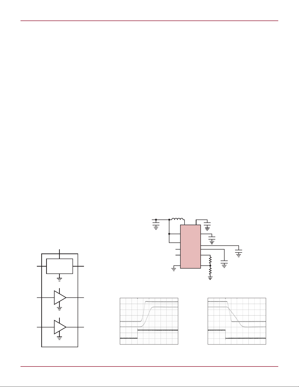
2.6V–5V Input to 34V Output
MEMS Driver
Figure 2 shows a MEMS driver that
takes a 2.6V–5V input and produces
a 34V output. This circuit draws very
little source current when the dual
half-bridge is disabled. The input
current is only 320µA at 2.6VIN and
128µA at 5VIN. A logic level signal at
IN1 and IN2 activates the dual halfbridge switches. Figure 3 shows the
turn-on delay and rise time for OUT1
and OUT2 with both half-bridges activated. Figure 4 shows the turn-off
delay and fall time with the 200pF
and 1nF capacitive loads shown in
Figure 2. See the data sheet details
for measuring delay time.
Figure 1. Simplified block diagram of the
LT8415
Linear Technology Magazine • September 2009
Figure 2. 2.6V–5V input to 34V dual half-bridge boost converter
Figure 3. Turn-on delay and rise time for OUT1
and OUT2
Figure 4. Turn-off delay and fall time for OUT1
and OUT2
3131
L DESIGN FEATURES
SW CAP
GND
FBP
OUT 2
OUT 1
IN 2
IN 1
LT8415
2.2µF
LOGIC
LEVEL
L1
100µH
0.1µF
1µF
16V
1.6mA AT 3V
IN
10mA AT 10V
IN
1nF
200pF
V
IN
3V to 10V
VCCV
OUT
V
REF
SHDN
604K
412K
16V/0V
16V/0V
L1: COILCRAFT DO2010-104ML
V
OUT1
(1.8V)
500mV/DIV
V
OUT2
(1.2V)
500mV/DIV
200µs/DIV
V
IN1
V
IN1
V
OUT1
1.8V
4A
V
OUT2
1.2V
4A
V
OUT1
V
OUT3
1V
1.5A
V
IN
5V
V
IN
V
OUT2
22µF
10µF
100µF
4.02k
10k
LTM4615
4.7µF
3.32k
V
IN2
P
GOOD1
P
GOOD2
V
OUT2
FB2
COMP2
V
OUT1
FB1
COMP1
TRACK1
RUN/SS1
LDO_IN
EN3
TRACK2
RUN/SS2
LDO_OUT
FB3
P
GOOD3
100µF
22µF
GND
10k
4.99k
10µF
=2
82µF
+
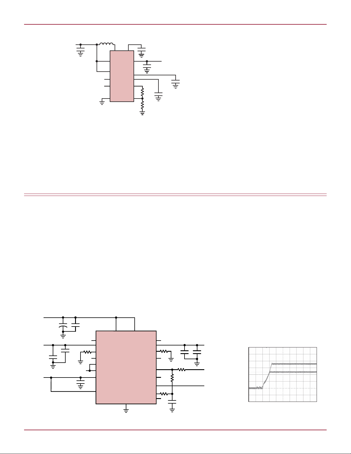
Figure 5. 3V–10V input to 16V dual half-bridge plus 16V output boost converter
3V–10V Input to 16V Output
MEMS Driver and Bias Supply
Figure 5 shows a 3V–10V input to
16V output converter, where the output drives the dual half-bridge and
also provides bias current for other
circuitry. The converter in Figure 2
can be used in a similar fashion, but
the current available at the output is
reduced as the output voltage is increased. See the data sheet for details
about maximum output current.
Integrated Resistor Divider
The LT8415 contains an integrated
resistor divider such that if the FBP
pin is at 1.235V or higher, the output
is clamped at 40V. For lower output
voltage levels use R1 and R2, calculating their values as instructed by the
data sheet. This method of setting the
output voltage ensures the voltage divider draws minimal current from the
input when the part is turned off.
Conclusion
The LT8415 is an ideal match for
driving low power MEMS. It integrates
a step-up converter power switch
and diode, a complementary dual
half-bridge, and a novel switching
architecture that minimizes power
dissipation.
L
LTM4614/15, continued from page 26
to promote good thermal conductivity.
Figure 10 shows that thermal dissipa
tion is well-balanced between the two
switching regulators.
Output Voltage Tracking
Tracking can be programmed using
the TRACK1 and TRACK2 pins. To
implement coincident tracking, at the
slave’s TRACK pin, divide the master
regulator’s output with a resistor
divider that is the same as the slave
regulator’s feedback divider. Figure 11
32
shows a tracking design and Figure 12
-
shows the output. V
in master-slave design with both
outputs ramping up coincidently. The
smooth start-up time is attributed to
the soft-start capacitor.
Conclusion
The cumbersome designs typical of
multivoltage regulation are a thing of
the past. The LTM4614 and LTM4615
µModule multiple-output regulators
can be easily fit into space-constrained
Figure 11. Output voltage tracking design example
OUT2
tracks V
OUT1
system boards with far fewer components than discrete solutions. The
dual-output LTM4614 µModule regulator and triple-output LTM4615 are
small in size, have excellent thermal
dissipation and have high efficiency.
Independent input and output voltage
rails give these µModule regulators
unmatched flexibility. They can be
used in a variety of input-output combinations, including input and output
current sharing, output voltage tracking, and low noise output.
Figure 12. Start-up waveforms for the circuit
in Figure 11
Linear Technology Magazine • September 2009
L
 Loading...