

LT6700-1/LT6700-2/LT6700-3/
LT6700HV-1/LT6700HV-2/
LT6700HV-3
Micropower, Low Voltage,
Dual Comparator with
400mV Reference
FEATURES
n
Internal 400mV Reference
n
Total Threshold Error: ±1.25% Max at 25°C
n
Inputs and Outputs Operate to 36V
n
Wide Supply Range: 1.4V to 18V
n
Specifi ed for –55°C to 125°C Temperature Range
n
Low Quiescent Current: 6.5µA Typ at 5V
n
Internal Hysteresis: 6.5mV Typ
n
Low Input Bias Current: ±10nA Max
n
Over-The-Top® Input also Includes Ground
n
Open-Collector Outputs Allow Level Translation
n
Choice of Input Polarities: LT6700-1/LT6700-2/
LT6700-3/LT6700HV-1/LT6700HV-2/LT6700HV-3
n
Available in Low Profi le (1mm) SOT-23 (ThinSOT™)
and 2mm × 3mm DFN Packages
APPLICATIONS
n
Battery-Powered System Monitoring
n
Threshold Detectors
n
Window Comparators
n
Relay Driving
n
Industrial Control Systems
n
Handheld Instruments
n
Automotive Monitor and Controls
L, LT, LTC and LTM are registered trademarks of Linear Technology Corporation. Over-The-Top
is a registered trademark of Linear Technology Corporation. ThinSOT is a trademark of Linear
Technology Corporation. All other trademarks are the property of their respective owners.
DESCRIPTION
The LT®6700-1/LT6700-2/LT6700-3/LT6700HV-1/
LT6700HV-2/LT6700HV-3 combine two micropower, low
voltage comparators with a 400mV reference in a 6-lead
SOT-23 or tiny DFN package. Operating with supplies from
1.4V up to 18V, these devices draw only 6.5µA, making
them ideal for low voltage system monitoring. Hysteresis
is included in the comparators, easing design requirements
to insure stable output operation.
The comparators each have one input available externally;
the other inputs are connected internally to the reference.
The comparator outputs are open collector and the output
load can be referred to any voltage up to 18V (36V for
LT6700HV), independent of supply voltage. The output
stage sinking capability is guaranteed to be greater than
5mA over temperature.
The three versions of this part differ by the polarity of the available comparator inputs. The LT6700-1/
LT6700HV-1 has one inverting input and one noninverting input, making it suitable for use as a window comparator. The LT6700-2/LT6700HV-2 has two inverting
inputs and the LT6700-3/LT6700HV-3 has two noninverting inputs. All versions are offered in commercial,
industrial and automotive temperature ranges.
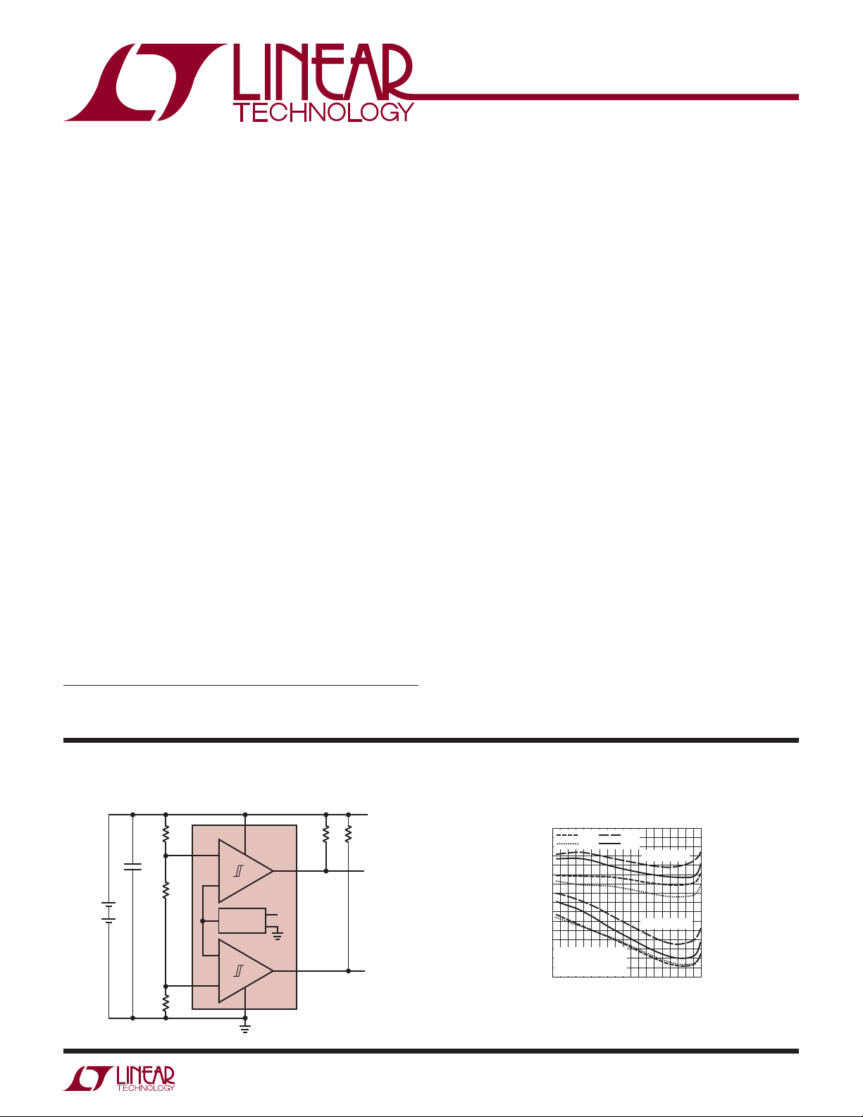
TYPICAL APPLICATION
Micropower Battery Monitor
LT6700-3
1M
COMP B
+
–
VR = 400mV
REFERENCE
COMP A
–
+
ALKALINE
AA CELLS
0.1µF
+
+
63.4k
261k
V
BATT
1.4V (MIN)
3V (NOM)
1M
1M
> 1.6V
V
BATT
V
S
> 2V
V
BATT
MONITOR CONSUMES ~10µA
HYSTERESIS IS APPROXIMATELY
2% OF TRIP VOLTAGE
6700123 TA01
Comparator Thresholds
vs Temperature
406
404
402
400
398
396
394
THRESHOLD VOLTAGE (mV)
392
390
#1A
#1B
TWO TYPICAL PARTS
COMP A AND B
= 5V
V
S
–60
–40 –20 0
#2A
#2B
20 40 60 80 100
TEMPERATURE (°C)
RISING INPUT
FALLING INPUT
120
6700123 TA02
6700123ff
1
LT6700-1/LT6700-2/LT6700-3/
LT6700HV-1/LT6700HV-2/
LT6700HV-3
ABSOLUTE MAXIMUM RATINGS
(Note 1)
Total Supply Voltage (VS to GND) ..........................18.5V
Input Voltage (+IN, –IN)
LT6700 (Note 3) .......................... 18.5V to (GND – 0.3V)
LT6700HV (Note 3) ........................ 40V to (GND – 0.3V)
LT6700 Output Voltage (OUT) ..... 18.5V to (GND – 0.3V)
LT6700HV Output Voltage (OUT) ... 40V to (GND – 0.3V)
Output Short-Circuit Duration (Note 2) ............ Indefi nite
Input Current (Note 3) ..........................................–10mA
Operating Temperature Range (Note 4)
LT6700CS6/LT6700HVCS6/
LT6700CDCB-1/-2/-3 ...........................–40°C to 85°C
LT6700IS6/LT6700HVIS6/
LT6700IDCB-1/-2/-3 ............................ –40°C to 85°C
LT6700HS6/LT6700HVHS6/
LT6700HDCB-1/-2/-3 ........................ –40°C to 125°C
PIN CONFIGURATION
Specifi ed Temperature Range (Note 5)
LT6700CS6/LT6700HVCS6/
LT6700CDCB-1/-2/-3 .............................. 0°C to 70°C
LT6700IS6/LT6700HVIS6/
LT6700IDCB-1/-2/-3 ............................ –40°C to 85°C
LT6700HS6/LT6700HVHS6/
LT6700HDCB-1/-2/-3 ....................... –40°C to 125°C
LT6700MPDCB-1/-2/-3 .................... –55°C to 125°C
Maximum Junction Temperature
S6 Package ....................................................... 150°C
DCB6 Package ..................................................150°C
Storage Temperature Range
S6 Package ........................................ –65°C to 150°C
DCB6 Package ...................................–65°C to 150°C
Lead Temperature, TSOT-23 (Soldering, 10 sec) ...300°C
LT6700-1
LT6700HV-1
TOP VIEW
OUTA 1
GND 2
+INA 3
S6 PACKAGE
6-LEAD PLASTIC TSOT-23
T
= 150°C, θJA = 230°C/W
JMAX
6 OUTB
5 V
S
4 –INB
LT6700-2
LT6700HV-2
OUTA 1
GND 2
–INA 3
TOP VIEW
S6 PACKAGE
6-LEAD PLASTIC TSOT-23
T
= 150°C, θJA = 230°C/W
JMAX
6 OUTB
5 V
S
4 –INB
LT6700-3
LT6700HV-3
LT6700-1 LT6700-2 LT6700-3
TOP VIEW
1
OUTA
2
OUTB
3
V
S
6-LEAD (2mm × 3mm) PLASTIC DFN
T
JMAX
SOLDERED EXPOSED PAD (PIN 7)
INTERNALLY CONNECTED TO GND
(PCB CONNECTION OPTIONAL)
7
DCB6 PACKAGE
= 125°C, θJA = 64°C/W
6
+ INA
5
GND
4
–INB
OUTA
OUTB
V
S
6-LEAD (2mm × 3mm) PLASTIC DFN
SOLDERED EXPOSED PAD (PIN 7)
INTERNALLY CONNECTED TO GND
TOP VIEW
1
2
3
T
JMAX
(PCB CONNECTION OPTIONAL)
7
DCB6 PACKAGE
= 125°C, θJA = 64°C/W
6
– INA
5
GND
4
–INB
OUTA
OUTB
V
6-LEAD (2mm × 3mm) PLASTIC DFN
TOP VIEW
OUTA 1
GND 2
+INA 3
S6 PACKAGE
6-LEAD PLASTIC TSOT-23
T
= 150°C, θJA = 230°C/W
JMAX
TOP VIEW
1
2
3
S
T
JMAX
SOLDERED EXPOSED PAD (PIN 7)
INTERNALLY CONNECTED TO GND
(PCB CONNECTION OPTIONAL)
7
DCB6 PACKAGE
= 125°C, θJA = 64°C/W
6 OUTB
5 V
4 +INB
S
6
+ INA
5
GND
4
+INB
2
6700123ff
LT6700-1/LT6700-2/LT6700-3/
LT6700HV-1/LT6700HV-2/
LT6700HV-3
ORDER INFORMATION
Lead Free Finish
TAPE AND REEL (MINI) TAPE AND REEL PART MARKING* PACKAGE DESCRIPTION SPECIFIED TEMPERATURE RANGE
LT6700CS6-1#TRMPBF LT6700CS6-1#TRPBF LTK7 6-Lead Plastic TSOT-23 0°C to 70°C
LT6700HVCS6-1#TRMPBF LT6700HVCS6-1#TRPBF LTK7 6-Lead Plastic TSOT-23 0°C to70°C
LT6700IS6-1#TRMPBF LT6700IS6-1#TRPBF LTK7 6-Lead Plastic TSOT-23 –40°C to 85°C
LT6700HVIS6-1#TRMPBF LT6700HVIS6-1#TRPBF LTK7 6-Lead Plastic TSOT-23 –40°C to 85°C
LT6700HS6-1#TRMPBF LT6700HS6-1#TRPBF LTK7 6-Lead Plastic TSOT-23 –40°C to 125°C
LT6700HVHS6-1#TRMPBF LT6700HVHS6-1#TRPBF LTK7 6-Lead Plastic TSOT-23 –40°C to 125°C
LT6700CS6-2#TRMPBF LT6700CS6-2#TRPBF LTADL 6-Lead Plastic TSOT-23 0°C to 70°C
LT6700HVCS6-2#TRMPBF LT6700HVCS6-2#TRPBF LTADL 6-Lead Plastic TSOT-23 0°C to 70°C
LT6700IS6-2#TRMPBF LT6700IS6-2#TRPBF LTADL 6-Lead Plastic TSOT-23 –40°C to 85°C
LT6700HVIS6-2#TRMPBF LT6700HVIS6-2#TRPBF LTADL 6-Lead Plastic TSOT-23 –40°C to 85°C
LT6700HS6-2#TRMPBF LT6700HS6-2#TRPBF LTADL 6-Lead Plastic TSOT-23 –40°C to 125°C
LT6700HVHS6-2#TRMPBF LT6700HVHS6-2#TRPBF LTADL 6-Lead Plastic TSOT-23 –40°C to 125°C
LT6700CS6-3#TRMPBF LT6700CS6-3#TRPBF LTADM 6-Lead Plastic TSOT-23 0°C to 70°C
LT6700HVCS6-3#TRMPBF LT6700HVCS6-3#TRPBF LTADM 6-Lead Plastic TSOT-23 0°C to 70°C
LT6700IS6-3#TRMPBF LT6700IS6-3#TRPBF LTADM 6-Lead Plastic TSOT-23 –40°C to 85°C
LT6700HVIS6-3#TRMPBF LT6700HVIS6-3#TRPBF LTADM 6-Lead Plastic TSOT-23 –40°C to 85°C
LT6700HS6-3#TRMPBF LT6700HS6-3#TRPBF LTADM 6-Lead Plastic TSOT-23 –40°C to 125°C
LT6700HVHS6-3#TRMPBF LT6700HVHS6-3#TRPBF LTADM 6-Lead Plastic TSOT-23 –40°C to 125°C
LT6700CDCB-1#TRMPBF LT6700CDCB-1#TRPBF LBXW
LT6700IDCB-1#TRMPBF LT6700IDCB-1#TRPBF LBXW
LT6700HDCB-1#TRMPBF LT6700HDCB-1#TRPBF LBXW
LT6700MPDCB-1#TRMPBF LT6700MPDCB-1#TR LDVS
LT6700CDCB-2#TRMPBF LT6700CDCB-2#TRPBF LBXX
LT6700IDCB-2#TRMPBF LT6700IDCB-2#TRPBF LBXX
LT6700HDCB-2#TRMPBF LT6700HDCB-2#TRPBF LBXX
LT6700MPDCB-2#TRMPBF LT6700MPDCB-2#TR LDVT
LT6700CDCB-3#TRMPBF LT6700CDCB-3#TRPBF LBXY
LT6700IDCB-3#TRMPBF LT6700IDCB-3#TRPBF LBXY
LT6700HDCB-3#TRMPBF LT6700HDCB-3#TRPBF LBXY
LT6700MPDCB-3#TRMPBF LT6700MPDCB-3#TR LDVV
TRM = 500 pieces. *Temperature grades are identifi ed by a label on the shipping container.
Consult LTC Marketing for parts specifi ed with wider operating temperature ranges.
Consult LTC Marketing for information on lead based fi nish parts.
For more information on lead free part marking, go to: http://www.linear.com/leadfree/
For more information on tape and reel specifi cations, go to: http://www.linear.com/tapeandreel/
6-Lead (2mm × 3mm) Plastic DFN
6-Lead (2mm × 3mm) Plastic DFN
6-Lead (2mm × 3mm) Plastic DFN
6-Lead (2mm × 3mm) Plastic DFN
6-Lead (2mm × 3mm) Plastic DFN
6-Lead (2mm × 3mm) Plastic DFN
6-Lead (2mm × 3mm) Plastic DFN
6-Lead (2mm × 3mm) Plastic DFN
6-Lead (2mm × 3mm) Plastic DFN
6-Lead (2mm × 3mm) Plastic DFN
6-Lead (2mm × 3mm) Plastic DFN
6-Lead (2mm × 3mm) Plastic DFN
0°C to 70°C
–40°C to 85°C
–40°C to 125°C
–55°C to 125°C
0°C to 70°C
–40°C to 85°C
–40°C to 125°C
–55°C to 125°C
0°C to 70°C
–40°C to 85°C
–40°C to 125°C
–55°C to 125°C
6700123ff
3

LT6700-1/LT6700-2/LT6700-3/
LT6700HV-1/LT6700HV-2/
LT6700HV-3
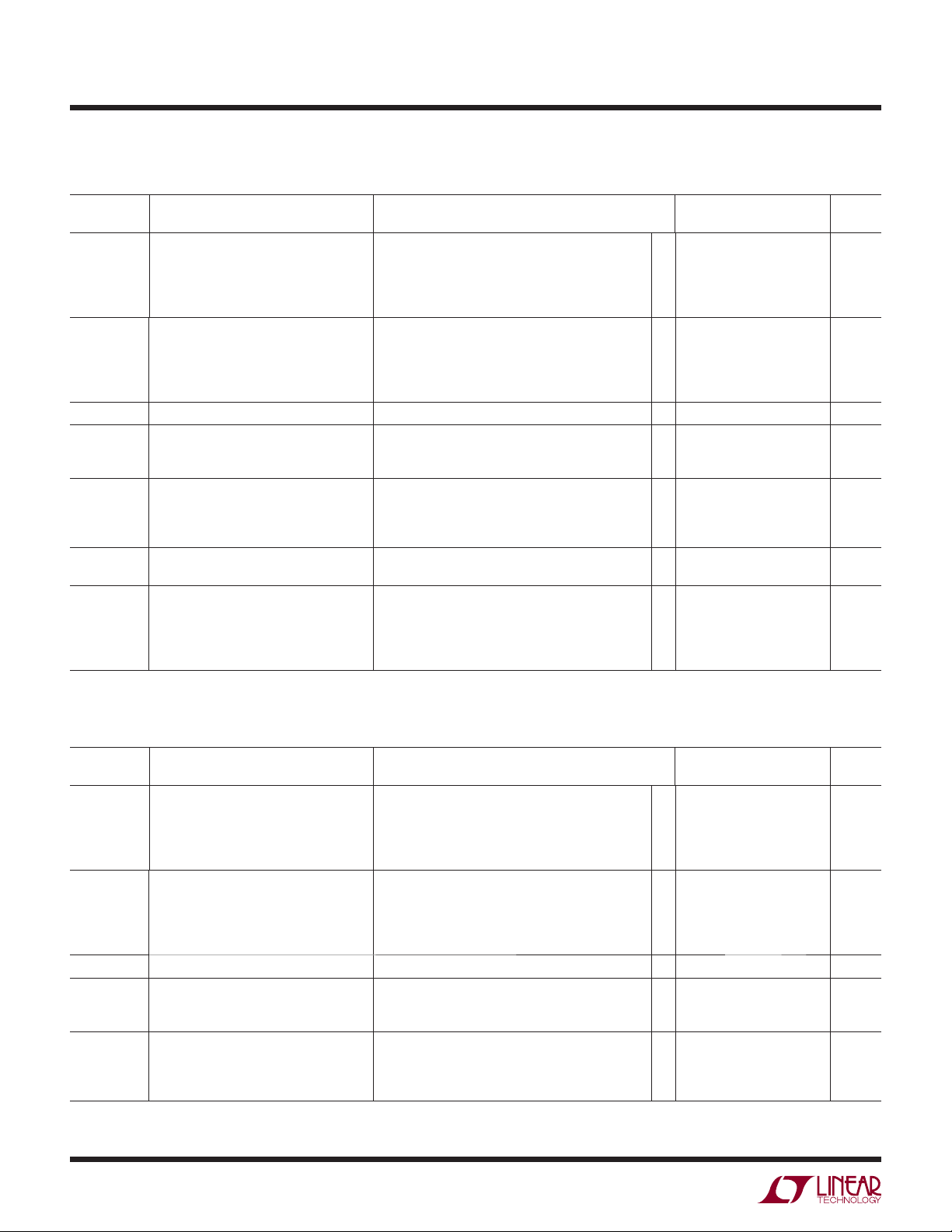
ELECTRICAL CHARACTERISTICS
T
SYMBOL PARAMETER CONDITIONS MIN TYP MAX UNITS
V
TH(R)
V
TH(F)
HYS HYS = V
I
B
V
OL
I
OFF
t
PD(HL)
t
PD(LH)
t
r
t
f
I
S
Rising Input Threshold Voltage (Note 6) RL = 100k, VO = 2V Swing
V
S
V
S
V
S
V
S
Falling Input Threshold Voltage (Note 6) RL = 100k, VO = 2V Swing
V
S
V
S
V
S
V
S
TH(R)
– V
TH(F)
VS = 1.4V, 5V, 12V, 18V, RL = 100k, VO = 2V Swing 3.5 6.5 9.5 mV
Input Bias Current VS = 1.4V, 18V, VIN = V
VS = 1.4V, VIN = 18V
V
S
Output Low Voltage 10mV Input Overdrive
V
S
V
S
V
S
Output Leakage Current VS = 1.4V, 18V, V
V
S
High-to-Low Propagation Delay VS = 5V, 10mV Input Overdrive, RL = 10k,
V
OL
Low-to-High Propagation Delay VS = 5V, 10mV Input Overdrive, RL = 10k,
V
OH
Output Rise Time VS = 5V, 10mV Input Overdrive, RL = 10k
V
O
Output Fall Time VS = 5V, 10mV Input Overdrive, RL = 10k
V
O
Supply Current No Load Current
V
S
V
S
V
S
V
S
= 25°C, (LT6700-1/LT6700-2/LT6700-3) unless otherwise specifi ed.
A
= 1.4V
= 5V
= 12V
= 18V
= 1.4V
= 5V
= 12V
= 18V
S
394
395
393
392
386
387
385
384
400
400
400
400
393.5
393.5
393.5
393.5
±0.01
±0.01
= 1.4V, 18V, VIN = 0.1V
= 1.4V, I
= 1.6V, I
= 5V, I
= 1.4V, V
= 0.5mA
OUT
= 3mA
OUT
= 5mA
OUT
= VS, VIN = 40mV Overdrive
OUT
= 18V, VIN = 40mV Overdrive
OUT
±4
55
60
70
0.01
0.01
18 µs
= 400mV
29 µs
= 0.9 • V
S
2.2 µs
= (0.1 to 0.9) • V
S
0.22 µs
= (0.1 to 0.9) • V
= 1.4V
= 5V
= 12V
= 18V
S
5.7
6.5
6.9
7.1
406
405
407
408
401
400
402
403
±10
±10
±10
200
200
200
0.8
0.8
10.0
11.0
12.5
13.0
mV
mV
mV
mV
mV
mV
mV
mV
nA
nA
nA
mV
mV
mV
µA
µA
µA
µA
µA
µA
l denotes the specifi cations which apply over the temperature range of 0°C ≤ T
The
≤ 70°C, (LT6700C-1/LT6700C-2/LT6700C-3) unless
A
otherwise specifi ed (Notes 4, 5).
SYMBOL PARAMETER CONDITIONS MIN TYP MAX UNITS
V
TH(R)
V
TH(F)
Rising Input Threshold Voltage (Note 6) RL = 100k, VO = 2V Swing
V
= 1.4V
S
V
= 5V
S
V
= 12V
S
V
= 18V
S
Falling Input Threshold Voltage (Note 6) RL = 100k, VO = 2V Swing
V
= 1.4V
S
V
= 5V
S
V
= 12V
S
V
= 18V
S
391.0
●
392.5
●
390.0
●
389.0
●
383.5
●
384.5
●
382.5
●
381.5
●
409.0
407.5
410.0
411.0
403.5
402.5
404.5
405.5
mV
mV
mV
mV
mV
mV
mV
mV
6700123ff
4
LT6700-1/LT6700-2/LT6700-3/
LT6700HV-1/LT6700HV-2/
LT6700HV-3
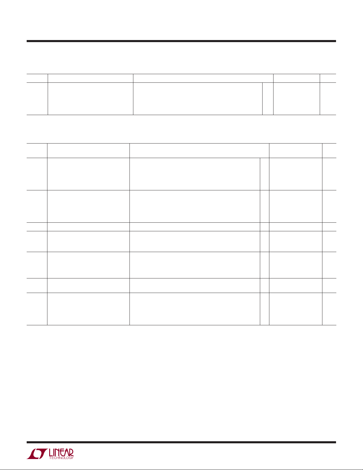
ELECTRICAL CHARACTERISTICS
The l denotes the specifi cations which apply over the temperature range of 0°C ≤ TA ≤ 70°C, (LT6700C-1/LT6700C-2/LT6700C-3) unless
otherwise specifi ed (Notes 4, 5).
SYMBOL PARAMETER CONDITIONS MIN TYP MAX UNITS
HYS HYS = V
I
B
V
OL
I
OFF
I
S
Input Bias Current VS = 1.4V, 18V, VIN = V
Output Low Voltage 10mV Input Overdrive
Output Leakage Current VS = 1.4V, 18V, V
Supply Current No Load Current
TH(R)
– V
TH(F)
VS = 1.4V, 5V, 12V, 18V, RL = 100k, VO = 2V Swing
VS = 1.4V, VIN = 18V
S
V
= 1.4V, 18V, VIN = 0.1V
S
V
= 1.4V, I
S
V
= 1.6V, I
S
V
= 5V, I
S
VS = 1.4V, V
V
= 1.4V
S
V
= 5V
S
V
= 12V
S
= 18V
V
S
= 0.5mA
OUT
= 3mA
OUT
= 5mA
OUT
= VS, VIN = 40mV Overdrive
OUT
= 18V, VIN = 40mV Overdrive
OUT
311mV
●
●
●
●
●
●
●
●
●
●
●
●
●
±15
±15
±15
250
250
250
1
1
13.0
14.0
15.5
16.0
nA
nA
nA
mV
mV
mV
µA
µA
µA
µA
µA
µA
The l denotes the specifi cations which apply over the temperature range of –40°C ≤ TA ≤ 85°C, (LT6700I-1/LT6700I-2/LT6700I-3)
unless otherwise specifi ed (Notes 4, 5).
SYMBOL PARAMETER CONDITIONS MIN TYP MAX UNITS
V
TH(R)
V
TH(F)
HYS HYS = V
I
B
V
OL
I
OFF
I
S
Rising Input Threshold Voltage (Note 6) RL = 100k, VO = 2V Swing
V
= 1.4V
S
V
= 5V
S
V
= 12V
S
V
= 18V
S
Falling Input Threshold Voltage (Note 6) RL = 100k, VO = 2V Swing
V
= 1.4V
S
V
= 5V
S
V
= 12V
S
V
= 18V
S
– V
TH(R)
TH(F)
Input Bias Current VS = 1.4V, 18V, VIN = V
VS = 1.4V, 5V, 12V, 18V, RL = 100k, VO = 2V Swing
S
VS = 1.4V, VIN = 18V
V
= 1.4V, 18V, VIN = 0.1V
S
Output Low Voltage 10mV Input Overdrive
V
= 1.4V, I
S
V
= 1.6V, I
S
V
= 5V, I
S
Output Leakage Current VS = 1.4V, 18V, V
V
= 1.4V, V
S
= 0.1mA
OUT
= 3mA
OUT
= 5mA
OUT
= VS, VIN = 40mV Overdrive
OUT
= 18V, VIN = 40mV Overdrive
OUT
Supply Current No Load Current
V
= 1.4V
S
V
= 5V
S
V
= 12V
S
V
= 18V
S
390
●
392
●
389
●
388
●
382.5
●
383.5
●
381.5
●
380.5
●
2 11.5 mV
●
●
●
●
●
●
●
●
●
●
●
●
●
410
408
411
412
404.5
403.5
405.5
406.5
±15
±15
±15
250
250
250
1
1
14.0
15.0
16.5
17.0
mV
mV
mV
mV
mV
mV
mV
mV
nA
nA
nA
mV
mV
mV
µA
µA
µA
µA
µA
µA
6700123ff
5
LT6700-1/LT6700-2/LT6700-3/
LT6700HV-1/LT6700HV-2/
LT6700HV-3
ELECTRICAL CHARACTERISTICS
The l denotes the specifi cations which apply over the temperature range of –40°C ≤ TA ≤ 125°C, (LT6700H-1/LT6700H-2/LT6700H-3)
unless otherwise specifi ed (Notes 4, 5).
SYMBOL PARAMETER CONDITIONS MIN
V
TH(R)
V
TH(F)
HYS HYS = V
I
B
V
OL
I
OFF
I
S
Rising Input Threshold Voltage (Note 6) RL = 100k, VO = 2V Swing
V
= 1.4V
S
V
= 5V
S
V
= 12V
S
V
= 18V
S
Falling Input Threshold Voltage (Note 6) RL = 100k, VO = 2V Swing
V
= 1.4V
S
V
= 5V
S
V
= 12V
S
V
= 18V
S
– V
TH(R)
TH(F)
Input Bias Current VS = 1.4V, 18V, VIN = V
VS = 1.4V, 5V, 12V, 18V, RL = 100k, VO = 2V Swing
S
VS = 1.4V, VIN = 18V
V
= 1.4V, 18V, VIN = 100mV
S
Output Low Voltage 10mV Input Overdrive
V
= 1.4V, I
S
V
= 1.6V, I
S
V
= 5V, I
S
Output Leakage Current VS = 1.4V, 18V, V
= 1.4V, V
V
S
= 0.1mA
OUT
= 3mA
OUT
= 5mA
OUT
= VS, VIN = 40mV Overdrive
OUT
= 18V, VIN = 40mV Overdrive
OUT
Supply Current No Load Current
V
= 1.4V
S
V
= 5V
S
V
= 12V
S
= 18V
V
S
●
●
●
●
●
●
●
●
●
●
●
●
●
●
●
●
●
●
●
●
●
LT6700H
TYP MAX UNITS
390
392
389
388
381.5
382.5
380.5
379.5
411
410
412
413
405.5
404.5
406.5
407.5
2 13.5 mV
±45
±45
±50
250
250
250
1
1
16.0
17.0
18.5
19.0
mV
mV
mV
mV
mV
mV
mV
mV
nA
nA
nA
mV
mV
mV
µA
µA
µA
µA
µA
µA
The l denotes the specifi cations which apply over the temperature range of –55°C ≤ TA ≤ 125°C, (LT6700MP-1/LT6700MP-2/LT6700MP-3)
unless otherwise specifi ed (Notes 4, 5).
SYMBOL PARAMETER CONDITIONS MIN
V
TH(R)
V
TH(F)
HYS HYS = V
I
B
V
OL
Rising Input Threshold Voltage (Note 6) RL = 100k, VO = 2V Swing
V
= 1.4V
S
V
= 5V
S
VS = 12V
V
= 18V
S
Falling Input Threshold Voltage (Note 6) RL = 100k, VO = 2V Swing
V
= 1.4V
S
V
= 5V
S
V
= 12V
S
V
= 18V
S
– V
TH(R)
TH(F)
Input Bias Current VS = 1.4V, 18V, VIN = V
VS = 1.4V, 5V, 12V, 18V, RL = 100k, VO = 2V Swing
S
VS = 1.4V, VIN = 18V
V
= 1.4V, 18V, VIN = 100mV
S
Output Low Voltage 10mV Input Overdrive
V
= 1.4V, I
S
V
= 1.6V, I
S
V
= 5V, I
S
OUT
= 0.1mA
OUT
= 3mA
OUT
= 5mA
●
●
●
●
●
●
●
●
●
●
●
●
●
●
●
LT6700H
TYP MAX UNITS
390
392
389
388
381.5
382.5
380.5
379.5
411
410
412
413
405.5
404.5
406.5
407.5
2 13.5 mV
±45
±45
±50
250
250
250
6700123ff
mV
mV
mV
mV
mV
mV
mV
mV
nA
nA
nA
mV
mV
mV
6

LT6700-1/LT6700-2/LT6700-3/
LT6700HV-1/LT6700HV-2/
LT6700HV-3
ELECTRICAL CHARACTERISTICS
The l denotes the specifi cations which apply over the temperature range of –55°C ≤ TA ≤ 125°C, (LT6700MP-1/LT6700MP-2/LT6700MP-3)
unless otherwise specifi ed (Notes 4, 5).
SYMBOL PARAMETER CONDITIONS MIN
I
OFF
I
S
Output Leakage Current VS = 1.4V, 18V, V
= 18V, V
V
S
OUT
Supply Current No Load Current
V
= 1.4V
S
V
= 5V
S
V
= 12V
S
= 18V
V
S
= VS, VIN = 40mV Overdrive
OUT
= 18V, VIN = 40mV Overdrive
●
●
●
●
●
●
TA = 25°C, (LT6700HV-1/LT6700HV-2/LT6700HV-3) unless otherwise specifi ed.
SYMBOL PARAMETER CONDITIONS MIN TYP MAX UNITS
V
TH(R)
V
TH(F)
HYS HYS = V
I
B
V
OL
I
OFF
t
PD(HL)
t
PD(LH)
t
r
t
f
I
S
Rising Input Threshold Voltage (Note 6) RL = 100k, VO = 2V Swing
V
= 1.4V
S
V
= 5V
S
V
= 12V
S
V
= 18V
S
Falling Input Threshold Voltage (Note 6) RL = 100k, VO = 2V Swing
V
= 1.4V
S
V
= 5V
S
V
= 12V
S
V
= 18V
S
– V
TH(R)
TH(F)
Input Bias Current VS = 1.4V, 18V, VIN = V
VS = 1.4V, 5V, 12V, 18V, RL = 100k, VO = 2V Swing 3.5 6.5 9.5 mV
S
VS = 1.4V, VIN = 18V, 36V
V
= 1.4V, 18V, VIN = 0.1V
S
Output Low Voltage 10mV Input Overdrive
V
= 1.4V, I
S
V
= 1.6V, I
S
V
= 5V, I
S
Output Leakage Current VS = 1.4V, 18V, V
V
= 18V, V
S
= 0.5mA
OUT
= 3mA
OUT
= 5mA
OUT
= VS, VIN = 40mV Overdrive
OUT
= 18V, (36V, RL = 100k), VIN = 40mV Overdrive
OUT
High-to-Low Propagation Delay VS = 5V, 10mV Input Overdrive, RL = 10k,
V
= 400mV
OL
Low-to-High Propagation Delay VS = 5V, 10mV Input Overdrive, RL = 10k,
V
= 0.9 • V
OH
S
Output Rise Time VS = 5V, 10mV Input Overdrive, RL = 10k
V
= (0.1 to 0.9) • V
O
S
Output Fall Time VS = 5V, 10mV Input Overdrive, RL = 10k
V
= (0.1 to 0.9) • V
O
S
Supply Current No Load Current
V
= 1.4V
S
VS = 5V
V
= 12V
S
V
= 18V
S
LT6700H
TYP MAX UNITS
394
395
393
392
386
387
385
384
400
400
400
400
393.5
393.5
393.5
393.5
±0.01
±0.01
±4
55
60
70
0.01
0.01
18 µs
29 µs
2.2 µs
0.22 µs
5.7
6.5
6.9
7.1
1
1
16.0
17.0
18.5
19.0
406
405
407
408
401
400
402
403
±10
±10
±10
200
200
200
0.8
0.8
10.0
11.0
12.5
13.0
µA
µA
µA
µA
µA
µA
mV
mV
mV
mV
mV
mV
mV
mV
nA
nA
nA
mV
mV
mV
µA
µA
µA
µA
µA
µA
6700123ff
7

LT6700-1/LT6700-2/LT6700-3/
LT6700HV-1/LT6700HV-2/
LT6700HV-3
ELECTRICAL CHARACTERISTICS
The l denotes the specifi cations which apply over the temperature range of 0°C ≤ TA ≤ 70°C, (LT6700HVC-1/LT6700HVC-2/LT6700HVC-3)
unless otherwise specifi ed (Notes 4, 5).
SYMBOL PARAMETER CONDITIONS MIN TYP MAX UNITS
V
TH(R)
Rising Input Threshold Voltage
(Note 6)
V
TH(F)
Falling Input Threshold Voltage
(Note 6)
HYS HYS = V
I
B
V
OL
I
OFF
I
S
Input Bias Current VS = 1.4V, 18V, VIN = V
Output Low Voltage 10mV Input Overdrive
Output Leakage Current VS = 1.4V, 18V, V
Supply Current No Load Current
TH(R)
– V
TH(F)
RL = 100k, VO = 2V Swing
V
= 1.4V
S
V
= 5V
S
V
= 12V
S
V
= 18V
S
RL = 100k, VO = 2V Swing
V
= 1.4V
S
V
= 5V
S
V
= 12V
S
V
= 18V
S
VS = 1.4V, 5V, 12V, 18V, RL = 100k, VO = 2V Swing
VS = 1.4V, VIN = 18V, 36V
S
V
= 1.4V, 18V, VIN = 0.1V
S
V
= 1.4V, I
S
V
= 1.6V, I
S
V
= 5V, I
S
V
= 18V, V
S
V
= 1.4V
S
V
= 5V
S
V
= 12V
S
= 18V
V
S
= 0.5mA
OUT
= 3mA
OUT
= 5mA
OUT
= VS, VIN = 40mV Overdrive
OUT
= 18V, (36V, RL = 100k), VIN = 40mV Overdrive
OUT
391.0
●
392.5
●
390.0
●
389.0
●
383.5
●
384.5
●
382.5
●
381.5
●
311mV
●
●
●
●
●
●
●
●
●
●
●
●
●
409.0
407.5
410.0
411.0
403.5
402.5
404.5
405.5
±15
±15
±15
250
250
250
1
1
13.0
14.0
15.5
16.0
mV
mV
mV
mV
mV
mV
mV
mV
nA
nA
nA
mV
mV
mV
µA
µA
µA
µA
µA
µA
The l denotes the specifi cations which apply over the temperature range of –40°C ≤ TA ≤ 85°C, (LT6700HVI-1/LT6700HVI-2/LT6700HVI-3)
unless otherwise specifi ed (Notes 4, 5).
SYMBOL PARAMETER CONDITIONS MIN TYP MAX UNITS
V
TH(R)
V
TH(F)
HYS HYS = V
I
B
V
OL
I
OFF
Rising Input Threshold Voltage (Note 6) RL = 100k, VO = 2V Swing
V
= 1.4V
S
V
= 5V
S
V
= 12V
S
V
= 18V
S
Falling Input Threshold Voltage (Note 6) RL = 100k, VO = 2V Swing
V
= 1.4V
S
V
= 5V
S
V
= 12V
S
V
= 18V
S
– V
TH(R)
TH(F)
Input Bias Current VS = 1.4V, 18V, VIN = V
VS = 1.4V, 5V, 12V, 18V, RL = 100k, VO = 2V Swing
S
VS = 1.4V, VIN = 18V, 36V
V
= 1.4V, 18V, VIN = 0.1V
S
Output Low Voltage 10mV Input Overdrive
V
= 1.4V, I
S
V
= 1.6V, I
S
V
= 5V, I
S
Output Leakage Current VS = 1.4V, 18V, V
V
= 18V, V
S
= 0.1mA
OUT
= 3mA
OUT
= 5mA
OUT
= VS, VIN = 40mV Overdrive
OUT
= 18V, (36V, RL = 100k), VIN = 40mV Overdrive
OUT
390
●
392
●
389
●
388
●
382.5
●
383.5
●
381.5
●
380.5
●
2 11.5 mV
●
●
●
●
●
●
●
●
●
410
408
411
412
404.5
403.5
405.5
406.5
±15
±15
±15
250
250
250
1
1
mV
mV
mV
mV
mV
mV
mV
mV
nA
nA
nA
mV
mV
mV
µA
µA
6700123ff
8
LT6700-1/LT6700-2/LT6700-3/
LT6700HV-1/LT6700HV-2/
LT6700HV-3
ELECTRICAL CHARACTERISTICS
The l denotes the specifi cations which apply over the temperature range of –40°C ≤ TA ≤ 85°C, (LT6700HVI-1/LT6700HVI-2/LT6700HVI-3)
unless otherwise specifi ed (Notes 4, 5).
SYMBOL PARAMETER CONDITIONS MIN TYP MAX UNITS
I
S
The l denotes the specifi cations which apply over the temperature range of –40°C ≤ TA ≤ 125°C, (LT6700HVH-1/LT6700HVH-2/
LT6700HVH-3) unless otherwise specifi ed (Notes 4, 5).
SYMBOL PARAMETER CONDITIONS MIN
V
TH(R)
V
TH(F)
HYS HYS = V
I
B
V
OL
I
OFF
I
S
Note 1: Stresses beyond those listed under Absolute Maximum Ratings
may cause permanent damage to the device. Exposure to any Absolute
Maximum Rating condition for extended periods may affect device
reliability and lifetime.
Note 2: A heat sink may be required to keep the junction temperature
below the absolute maximum rating when the output is shorted
indefi nitely.
Note 3: The inputs are protected by ESD diodes to the ground. If the input
voltage exceeds –0.3V below ground, the input current should be limited
to less than 10mA.
Note 4: The LT6700C-1/-2/-3/LT6700HVC-1/-2/-3, and
LT6700I-1/-2/-3/LT6700HVI-1/-2/-3 are guaranteed functional over the
operating temperature range of –40°C to 85°C. The LT6700H-1/-2/-3/
LT6700HVH-1/-2/-3 is guaranteed functional over the operating
Supply Current No Load Current
V
= 1.4V
S
V
= 5V
S
V
= 12V
S
V
= 18V
S
Rising Input Threshold Voltage
(Note 6)
Falling Input Threshold Voltage
(Note 6)
– V
TH(R)
TH(F)
RL = 100k, VO = 2V Swing
V
= 1.4V
S
V
= 5V
S
V
= 12V
S
V
= 18V
S
RL = 100k, VO = 2V Swing
V
= 1.4V
S
V
= 5V
S
V
= 12V
S
V
= 18V
S
VS = 1.4V, 5V, 12V, 18V, RL = 100k, VO = 2V Swing
Input Bias Current VS = 1.4V, 18V, VIN = V
VS = 1.4V, VIN = 18V, 36V
V
= 1.4V, 18V, VIN = 100mV
S
Output Low Voltage 10mV Input Overdrive
V
= 1.4V, I
S
V
= 1.6V, I
S
V
= 5V, I
S
Output Leakage Current VS = 1.4V, 18V, V
V
= 18V, V
S
= 0.1mA
OUT
= 3mA
OUT
= 5mA
OUT
= VS, VIN = 40mV Overdrive
OUT
= 18V, (36V, RL = 100k), VIN = 40mV Overdrive
OUT
Supply Current No Load Current
V
= 1.4V
S
V
= 5V
S
V
= 12V
S
= 18V
V
S
●
●
●
●
14.0
15.0
16.5
17.0
LT6700H
TYP MAX UNITS
390
●
392
●
389
●
388
●
381.5
●
382.5
●
380.5
●
379.5
●
2 13.5 mV
●
S
●
●
●
●
●
●
●
●
●
●
●
●
411
410
412
413
405.5
404.5
406.5
407.5
±45
±45
±50
250
250
250
1
1
16.0
17.0
18.5
19.0
temperature range of –40°C to 125°C. The LT6700MP-1/-2/-3 is
guaranteed functional over the operating temperature range of –55°C to
125°C.
Note 5: The LT6700C-1/-2/-3/LT6700HVC-1/-2/-3 is guaranteed to
meet the specifi ed performance from 0°C to 70°C. The LT6700C-1/-2/3/LT6700HVC-1/-2/-3 are designed, characterized and expected to meet
specifi ed performance from –40°C to 85°C but are not tested or QA
sampled at these temperatures. The LT6700I-1/-2/-3/LT6700HVI-1/-2/-3
is guaranteed to meet specifi ed performance from –40°C to 85°C. The
LT6700H-1/-2/-3/LT6700HVH-1/-2/-3 is guaranteed to meet specifi ed
performance from –40°C to 125°C.The LT6700MP-1/-2/-3 is guaranteed to
meet specifi ed performance from –55°C to 125°C.
Note 6: V
defi nes the threshold voltage of the comparators and
TH
combines the effect of offset and reference accuracy.
µA
µA
µA
µA
mV
mV
mV
mV
mV
mV
mV
mV
nA
nA
nA
mV
mV
mV
µA
µA
µA
µA
µA
µA
6700123ff
9

LT6700-1/LT6700-2/LT6700-3/
LT6700HV-1/LT6700HV-2/
LT6700HV-3
PIN FUNCTIONS
V
–
+
400mV
REFERENCE
+
–
GND
–INB
+INA
LT6700-1
LT6700HV-1
–
+
–
+
V
S
COMP B
400mV
REFERENCE
COMP A
GND
LT6700-2
LT6700HV-2
–INB
OUTB
V
S
OUTA
–INA
6700123 PF01
OUTA: Open-Collector Output of Comparator Section A.
This pin provides drive for up to 40mA of load current. Offstate voltage may be as high as 18V (36V for LT6700HV)
above GND, regardless of VS used.
GND: Ground. This pin is also the low side return of the
internal 400mV reference.
INA: External Input for Comparator Section A. The voltage on this pin can range from –0.3V to 18V (36V for
LT6700HV) with respect to GND regardless of VS used.
The input is noninverting for the LT6700-1/LT6700HV-1
and LT6700-3/LT6700HV-3, and inverting for the LT6700-2/
LT6700HV-2. The other section A comparator input is
internally connected to the 400mV reference.
V
S
COMP B
LT6700-3
LT6700HV-3
+INB
OUTB
S
COMP B
+
OUTB
–
COMP A
V
S
400mV
REFERENCE
–
OUTA
+INA
6700123 PF02
+
GND
COMP A
V
S
OUTA
6700123 PF03
INB: External Input for Comparator Section B. The voltage on this pin can range from –0.3V to 18V (36V for
LT6700HV) with respect to GND regardless of VS used.
The input is noninverting for the LT6700-3/LT6700HV-3,
and inverting for the LT6700-1/LT6700HV-1 and LT6700-2/
LT6700HV-2. The other section B comparator input is
internally connected to the 400mV reference.
VS: Comparator Core Supply Voltage. The parts are characterized for operation with 1.4V ≤ VS ≤ 18V with respect
to GND.
OUTB : Open-Collector Output of Comparator Section B.
This pin provides drive for up to 40mA of load current. Offstate voltage may be as high as 18V (36V for LT6700HV)
above GND, regardless of V
used.
S
10
6700123ff

LT6700-1/LT6700-2/LT6700-3/
LT6700HV-1/LT6700HV-2/
TYPICAL PERFORMANCE CHARACTERISTICS
LT6700HV-3
Distribution of Rising Input
Threshold Voltage
18
VS = 5V
= 25°C
T
16
A
14
12
10
8
6
PERCENT OF UNITS (%)
4
2
0
394 396 398 400 402 404 406
RISING INPUT THRESHOLD VOLTAGE (mV)
Rising Input Threshold Voltage
vs Temperature
404
403
402
401
400
399
398
397
RISING INPUT THRESHOLD VOLTAGE (mV)
396
–60 –40
–20
FOUR TYPICAL PARTS
= 5V
V
#1
#2
#3
#4
TEMPERATURE (°C)
S
0 20406080
6700123 G01
100 120
6700123 G04
Distribution of Falling Input
Threshold Voltage Distribution of Hysteresis
18
16
14
12
10
8
6
PERCENT OF UNITS (%)
4
2
0
388 390 392 394 396 398 400
FALLING INPUT THRESHOLD VOLTAGE (mV)
Rising Input Threshold Voltage
vs Temperature
403.0
402.5
402.0
401.5
401.0
400.5
400.0
399.5
RISING INPUT THRESHOLD VOLTAGE (mV)
399.0
–60 –40
VS = 1.4V
= 5V
V
S
= 12V
V
S
= 18V
V
S
0 20406080
–20
TEMPERATURE (°C)
VS = 5V
= 25°C
T
A
6700123 G02
100 120
6700123 G05
20
VS = 5V
18
= 25°C
T
A
16
14
12
10
8
6
PERCENT OF UNITS (%)
4
2
0
4 4.8 5.6 6.4 7.2 8 8.8
HYSTERESIS (mV)
Rising Input Threshold Voltage
vs Supply Voltage
403.0
402.5
402.0
401.5
401.0
400.5
400.0
399.5
RISING INPUT THRESHOLD VOLTAGE (mV)
399.0
TA = 25°C
= 85°C
T
A
= 125°C
T
A
= –55°C
T
A
24 1614 18
6
SUPPLY VOLTAGE (V)
6700123 G03
81012
6700123 G06
Hysteresis vs Temperature Hysteresis vs Temperature Hysteresis vs Supply Voltage
10
FOUR TYPICAL PARTS
= 5V
V
S
9
8
7
6
5
HYSTERESIS (mV)
4
3
2
–60 –40
#1
#2
#3
#4
–20
0 20406080
TEMPERATURE (°C)
100 120
6700123 G07
10
9
8
7
6
5
HYSTERESIS (mV)
4
3
2
–60 –40
VS = 1.4V
V
V
V
–20
= 5V
S
= 12V
S
= 18V
S
0 20406080
TEMPERATURE (°C)
100 120
6700123 G08
10
9
8
7
6
5
HYSTERESIS (mV)
4
3
2
TA = 25°C
= 85°C
T
A
24 1614 18
81012
6
SUPPLY VOLTAGE (V)
TA = 125°C
= –55°C
T
A
6700123 G09
6700123ff
11

LT6700-1/LT6700-2/LT6700-3/
LT6700HV-1/LT6700HV-2/
LT6700HV-3
TYPICAL PERFORMANCE CHARACTERISTICS
Quiescent Supply Current
Minimum Supply Voltage
1
0
–1
–2
–3
THRESHOLD SHIFT (mV)
–4
–5
1.3 1.7
SUPPLY VOLTAGE (V)
TA = 25°C
= 85°C
T
A
= 125°C
T
A
= –55°C
T
A
1.91.10.9 1.5
6700123 G10
vs Supply Voltage Start-Up Supply Current
10
9
8
7
6
SUPPLY CURRENT (µA)
5
4
TA = 25°C
= 85°C
T
A
NO LOAD CURRENT
1.4 3.4
5.4
SUPPLY VOLTAGE (V)
7.4 9.4 11.4
TA = 125°C
= –55°C
T
A
15.413.4 17.4
6700123 G11
50
40
30
20
SUPPLY CURRENT (µA)
10
0
TA = 25°C
= 85°C
T
A
= 125°C
T
A
= –55°C
T
A
0.2
0
0.4
SUPPLY VOLTAGE (V)
0.6
0.8
1.0 1.2
1.4
6700123 G12
Supply Current
vs Output Sink Current
1000
TA = –40°C
= 1.4V
V
S
= 5V
V
S
= 12V
V
S
= 18V
V
100
10
SUPPLY CURRENT (µA)
1
0.001 0.1 1 10
S
0.01
OUTPUT SINK CURRENT (mA)
100
6700123 G13
Supply Current
vs Output Sink Current
1000
TA = 25°C
= 1.4V
V
S
= 5V
V
S
= 12V
V
S
= 18V
V
100
10
SUPPLY CURRENT (µA)
1
0.001 0.1 1 10
S
0.01
OUTPUT SINK CURRENT (mA)
6700123 G14
100
Supply Current
vs Output Sink Current
1000
TA = 85°C
= 1.4V
V
S
= 5V
V
S
= 12V
V
S
= 18V
V
100
10
SUPPLY CURRENT (µA)
1
0.001 0.1 1 10
S
0.01
OUTPUT SINK CURRENT (mA)
Below Ground Input Bias Current Low Level Input Bias Current High Level Input Bias Current
10000
1000
100
10
INPUT BIAS CURRENT (nA)
CURRENT IS GOING OUT OF THE DEVICE
1
–0.3 –0.1 0
–0.2
INPUT VOLTAGE (V)
VS = 18V
–0.3V < V
< 0V
IB
TA = 25°C
= 85°C
T
A
= 125°C
T
A
= –55°C
T
A
6700123 G16
3
CURRENT IS POSITIVE GOING
2
INTO THE DEVICE
1
0
–1
–2
–3
–4
INPUT BIAS CURRENT (nA)
–5
–6
–7
0
0.1 0.3
0.4
0.2
INPUT VOLTAGE (V)
0.5
VS = 18V
0V < V
0.7
0.6
< 1V
IB
TA = 25°C
= 85°C
T
A
= 125°C
T
A
= –55°C
T
A
6700123 G17
10
1
0.1
0.01
INPUT BIAS CURRENT (nA)
0.001
10.90.8
CURRENT IS GOING INTO THE DEVICE
VS = 18V
> 1V
V
IB
TA = 25°C
= 85°C
T
A
= 125°C
T
A
1 3 5 7 9 11 13 15 17
INPUT VOLTAGE (V)
100
6700123 G15
6700123 G18
12
6700123ff

LT6700-1/LT6700-2/LT6700-3/
LT6700HV-1/LT6700HV-2/
TYPICAL PERFORMANCE CHARACTERISTICS
LT6700HV-3
Output Saturation Voltage
vs Output Sink Current
1000
TA = –40°C
= 1.4V
V
S
= 5V
V
S
= 12V
V
S
= 18V
V
100
10
OUTPUT SATURATION VOLTAGE (mV)
1
0.001 0.1 1 10
S
0.01
OUTPUT SINK CURRENT (mA)
100
6700123 G19
Output Saturation Voltage
vs Output Sink Current
1000
TA = 25°C
= 1.4V
V
S
= 5V
V
S
= 12V
V
S
= 18V
V
100
10
OUTPUT SATURATION VOLTAGE (mV)
1
0.001 0.1 1 10
S
0.01
OUTPUT SINK CURRENT (mA)
6700123 G20
100
Output Saturation Voltage
vs Output Sink Current
1000
TA = 85°C
= 1.4V
V
S
= 5V
V
S
= 12V
V
S
= 18V
V
100
10
OUTPUT SATURATION VOLTAGE (mV)
1
0.001 0.1 1 10
S
0.01
OUTPUT SINK CURRENT (mA)
Output Short-Circuit Current Output Short-Circuit Current Output Leakage Current
80
70
60
50
40
30
20
SHORT-CIRCUIT CURRENT (mA)
10
0
0
24 1614 18
81012
6
OUTPUT VOLTAGE (V)
80
70
60
50
TA = 25°C
= 1.4V
V
S
= 5V
V
40
30
= 5V
V
S
TA = 25°C
= 85°C
T
A
= 125°C
T
A
= –55°C
T
A
6700123 G22
20
SHORT-CIRCUIT CURRENT (mA)
10
0
0
24 1614 18
S
= 12V
V
S
= 18V
V
S
6
OUTPUT VOLTAGE (V)
81012
6700123 G23
10
1
0.1
0.01
OUTPUT LEAKAGE CURRENT (nA)
0.001
0 8 10 12 14 16
= 5V
V
S
TA = 25°C
T
T
T
246
OUTPUT VOLTAGE (V)
= 85°C
A
= 125°C
A
= –55°C
A
100
6700123 G21
18
6700123 G24
Propagation Delay
vs Input Overdrive
60
TA = 25°C
50
40
30
20
PROPAGATION DELAY (µs)
10
0
20
0
INPUT OVERDRIVE (mV)
Rise and Fall Times
vs Output Pull-Up Resistor
100
LH NONINV
HL NONINV
LH INV
HL INV
60
80
40
100
6700123 G25
VS = 5V
= 20pF
C
L
= 25°C
T
A
10
1
0.1
RISE AND FALL TIME (µs)
0.01
0.1
1 10 100 1000
OUTPUT PULL-UP RESISTOR (kΩ)
RISE
FALL
10mV/DIV
6700123 G26
Noninverting and Inverting
Comparator Propagation Delay
V
O(NINV)
5V/DIV
DC
V
O(INV)
5V/DIV
DC
V
IN
AC
= 15V
S
= 25°C
T
A
= 10k CONNNECTED TO V
R
LOAD
V
IN(OVERDRIVE)
VOLTAGE THRESHOLDS
20µs/DIVV
= 10mV OVER THE INPUT
6700123 G27
S
6700123ff
13

LT6700-1/LT6700-2/LT6700-3/
LT6700HV-1/LT6700HV-2/
LT6700HV-3
APPLICATIONS INFORMATION
The LT6700-1/LT6700-2/LT6700-3/LT6700HV-1/
LT6700HV-2/LT6700HV-3 devices are a family of dual
micropower comparators with a built-in 400mV reference. Features include wide supply voltage range (1.4V to
18V), Over-The-Top input and output range, 2% accurate
rising input threshold voltage and 6.5mV typical built-in
hysteresis. The comparator’s open-collector outputs can
sink up to 40mA typical.
Internal Reference
Each of the comparator sections has one input available
externally, with the three versions of the part differing by
the polarity of those available inputs (i.e., inverting or
noninverting). The other comparator inputs are connected
internally to the 400mV reference. The rising input threshold
voltage of the comparators is designed to be equal to that
of the reference (i.e., ≈400mV). The reference voltage is
established with respect to the device GND connection.
Hysteresis
Each comparator has built-in 6.5mV (typical) hysteresis to
simplify designs, ensure stable operation in the presence
of noise at the inputs, and to reject supply rail noise that
might be induced by state change load transients. The
hysteresis is designed such that the falling input threshold
voltage is nominally 393.5mV. External positive feedback
circuitry can be employed with noninverting comparator
inputs to increase effective hysteresis if desired, but such
circuitry will provide an apparent effect on both the rising
and falling input thresholds (the actual internal thresholds
remain unaffected).
Comparator Inputs
A comparator input can swing from ground to 18V (36V
for LT6700HV), regardless of the supply voltage used. The
typical input current for inputs well above threshold (i.e.,
> 800mV) is a few pA leaking into an input. With decreasing
input voltage, a small bias current begins to be drawn out
of the input, reaching a few nA when at ground potential.
The input may be forced 100mV below ground without
causing an improper output, though some additional bias
current will begin to fl ow from the parasitic ESD input protection diode. Inputs driven further negative than 100mV
below ground will not cause comparator malfunction or
damage (provided the current is limited to 10mA), but
the accuracy of the reference cannot be guaranteed, in
which case the output state of the alternate comparator
may be affected.
Comparator Outputs
The comparator outputs are open collector and capable
of sinking 40mA typical. Load currents are directed out
the GND pin of the part. The output off-state voltage may
range between –0.3V and 18V (36V for LT6700HV) with
respect to ground, regardless of the supply voltage used.
When the output high state bias voltage is above 18V, a
100k minimum pull-up resistor is required and total load
capacitor must be less than 100nF. If the output high state
is above 18V, caution must be taken to prevent a short
from the output directly to the bias voltage, even if the
output is in the off state. As with any open-collector device,
the outputs may be tied together to implement wire-AND
logic functions.
14
6700123ff

APPLICATIONS INFORMATION
LT6700-1/LT6700-2/LT6700-3/
LT6700HV-1/LT6700HV-2/
LT6700HV-3
Power Supplies
The comparator family core circuitry operates from a single
1.4V to 18V supply. A minimum 0.1µF bypass capacitor
is required between the V
pin and GND. When an output
S
load is connected to the supply rail near the part and the
output is sinking more than 5mA, a 1µF bypass capacitor is
recommended. In instances where the supply is relatively
“soft” (such as with small batteries) and susceptible to
load steps, an additional 47 series decoupling resistor
can further improve isolation of supply transients from
pin.
the V
S
Flexible Window Comparator
Using the LT6700-1/LT6700HV-1 as shown in the circuits
of Figure 1, the wire-AND confi guration permits high
accuracy window functions to be implemented with a
3.3V Supply Monitor 5V Supply Monitor
3.3V
R3
301k
0.1µF 0.1µF
R2
6.04k
R1
40.2k
V
S
+INA
OUTA
LT6700-1
–INB OUTB
GND
33k
V
OUT
V
V
L
H
V
S
V
OUT
HIGH = (3.1V < VS < 3.5V)
HYSTERESIS ZONES
APPROXIMATELY
2% OF TRIP VOLTAGE
simple 3-resistor voltage divider network. The section A
comparator provides the V
comparator provides the V
trip-point and the section B
L
trip-point, with the built-in
H
hysteresis providing about 1.7% recovery level at each
trip point to prevent output chatter.
For designs that are to be optimized to detect
departure
from a window limit, the nominal resistor divider values
are selected as follows (refer to the resistor designators
shown on the fi rst circuit of Figure 1):
R1 ≤ 400k (this sets the divider current >> I
R2 = R1 • (0.98 • V
R3 = R1 • (2.5 • V
– 1)
H/VL
– 0.98 • VH/VL)
H
To create window functions optimized for detecting
of inputs)
B
entry
into a window (i.e., where the output is to indicate a “com-
5V
487k
6.04k
40.2k
V
S
+INA
OUTA
LT6700-1
–INB OUTB
GND
33k
V
OUT
HIGH = (4.7V < VS < 5.3V)
6700123 F01
Figure 1. Simple Window Comparator
6700123ff
15

LT6700-1/LT6700-2/LT6700-3/
LT6700HV-1/LT6700HV-2/
LT6700HV-3
APPLICATIONS INFORMATION
ing into spec” condition, as with the examples in Figure 1),
the nominal resistor values are selected as follows:
R1 ≤ 400k (this sets the divider current >> I
R2 = R1 • (1.02 • V
R3 = R1 • (2.54 • V
– 1)
H/VL
– 1.02 • VH/VL)
H
of inputs)
B
The worst-case variance of the trip-points is related to
the specifi ed threshold limits of the LT6700/LT6700HV
device and the basic tolerance of divider resistors used.
For resistor tolerance R
case trip-point voltage (either V
(e.g. 0.01 for 1%), the worst-
TOL
or VL) deviations can be
H
predicted as follows (italicized values are taken from the
datasheet, expressed in volts):
Max dev V
/ V
TRIPnom
Max dev V
/ V
TRIPnom
= ±V
TRIP↑
] + 1.25 • (
= ±V
TRIP↓
] + 1.27 • (
TRIPnom
TRIPnom
V
TH(R)max
V
TH(F)max
• {2 • R
–
• {2 • R
–
• [(V
TOL
V
TH(R)min
• [(V
TOL
V
TH(F)min
TRIPnom
)}
TRIPnom
)}
– 0.4)
– 0.39)
Generating an External Reference Signal
In some applications, it would be advantageous to have
access to a signal that is directly related to the internal
400mV reference, even though the reference itself is not
available externally. This can be accomplished to a reasonable degree by using an inverting comparator section as
a “bang-bang” servo, establishing a nominal voltage, on
an integration capacitor, that is scaled to the reference.
This method is used in Figure 2, where the reference level
has been doubled to drive a resistor bridge. The section
B output cycles on and off to swing the section B input
between its hysteresis trip points as the load capacitor
charges and discharges in a shallow, controlled fashion.
The multiplied reference signal also contains ripple that is
the hysteresis multiplied by the same factor, so additional
fi ltering is performed at the sense node of the bridge to
prevent comparator chatter in the section A comparator,
which is performing the actual conditional decision for
the circuit.
0.1µF
1.4V TO 18V
≈ 10µA)
(I
2 • V
REF
R
499k 220k 220k*
SET
R
TH
R
= 1M (e.g., YSI 44015, 1.00MΩ AT 25°C)
TH
= RTH AT T
R
SET
*RESISTANCE MAY REQUIRE OPTIMIZATION FOR OPERATION
OVER INTENDED R
HYSTERESIS ZONE ≈0.4°C
Figure 2. Micropower Thermostat/Temperature Alarm
499k
T
SET
AND V
TH
V
S
+INA
OUTA
LT6700-1
–INB OUTB
GND
RANGES
SUPPLY
10k
6700123 F02
S
T < T
3.3µF3.3µF
SET
16
6700123ff

APPLICATIONS INFORMATION
LT6700-1/LT6700-2/LT6700-3/
LT6700HV-1/LT6700HV-2/
LT6700HV-3
Instrumentation Grade Pulse Width Modulator (PWM)
Comparators with hysteresis are frequently employed
to make simple oscillator structures, and the LT6700/
LT6700HV lends itself nicely to forming a charge-balancing
PWM function. The circuit shown in Figure 3 forms a PWM
that is intended to transmit an isolated representation of a
voltage difference, rather like an isolated instrumentation
amplifi er. The section B comparator is used to generate a
2V reference supply level for the CMOS NOT gate (inverter),
which serves as the precision switch element for the charge
balancer. The heart of the charge balancer is the section A
comparator, which is detecting slight charge or discharge
states on the 0.22µF “integration” capacitor as it remains
balanced at ≈400mV by feedback through the NOT gate.
The input sense voltage, VIN, is converted to an imbal-
3V NOM (I
S
+
Lithium
COIN CELL
470Ω
412k*
††
100k*100k*
PWM(MAX)
V
S
+INA
OUTA
LT6700-1
–INB OUTB
GND
≈ 0.6kHz
22µF
+
V
IN
0V TO 2V
–
10k**
5 • V
= 2V
REF
NC7S14
309k*
1% METAL FILM
*
DELETE FOR PWM MODE
**
†
CONNECT FOR PWM MODE
††
OPTIMIZED FOR 2kHz ΔΣ SAMPLING, f
309k*
0.22µF
ance current that the NOT gate duty cycle is continually
correcting for, thus the digital waveform at the section A
comparator output is a PWM representation of VIN with
respect to the 2V “full scale.” In this particular circuit, the
PWM information drives the LED of an optocoupler, allowing the VIN information to be coupled across a dielectric
barrier. As an additional option to the circuit, the feedback
loop can be broken and a second optocoupler employed to
provide the charge balance management. This confi guration allows for clocking the comparator output (externally
to this circuit) and providing synchronous feedback such
that a simple ∆∑ voltage-to-frequency conversion can be
formed if desired. Approximately 11-bit accuracy and noise
performance was observed in a one second integration
period for duty factors from 1% to 99%.
1
2
6
5
3V/5V
10k
6
5
3V/5V
750**
1
2
ΔΣ
SAMPLE
IN
PWM OUT
(OR ΔΣ SENSE)
MOC-207
MOC-207**
< 3mA)
0.1µF
10k
0.1µF
750Ω
10k 10k
†
6700123 F03
Figure 3. Isolated PWM or Δ∑ Converter
6700123ff
17

LT6700-1/LT6700-2/LT6700-3/
LT6700HV-1/LT6700HV-2/
LT6700HV-3
PACKAGE INFORMATION
DCB Package
6-Lead Plastic DFN (2mm × 3mm)
(Reference LTC DWG # 05-08-1715)
0.70 ±0.05
3.55 ±0.05
2.15 ±0.05
1.65 ±0.05
(2 SIDES)
PACKAGE
OUTLINE
0.25 ± 0.05
0.50 BSC
1.35 ±0.05
(2 SIDES)
RECOMMENDED SOLDER PAD PITCH AND DIMENSIONS
2.00 ±0.10
(2 SIDES)
3.00 ±0.10
(2 SIDES)
PIN 1 BAR
TOP MARK
(SEE NOTE 6)
0.200 REF
0.75 ±0.05
0.00 – 0.05
R = 0.115
R = 0.05
1.65 ± 0.10
(2 SIDES)
TYP
TYP
1.35 ±0.10
BOTTOM VIEW—EXPOSED PAD
3
(2 SIDES)
0.40 ± 0.10
64
1
0.50 BSC
PIN 1 NOTCH
R0.20 OR 0.25
× 45° CHAMFER
(DCB6) DFN 0405
0.25 ± 0.05
18
NOTE:
1. DRAWING TO BE MADE A JEDEC PACKAGE OUTLINE M0-229 VARIATION OF (TBD)
2. DRAWING NOT TO SCALE
3. ALL DIMENSIONS ARE IN MILLIMETERS
4. DIMENSIONS OF EXPOSED PAD ON BOTTOM OF PACKAGE DO NOT INCLUDE
MOLD FLASH. MOLD FLASH, IF PRESENT, SHALL NOT EXCEED 0.15mm ON ANY SIDE
5. EXPOSED PAD SHALL BE SOLDER PLATED
6. SHADED AREA IS ONLY A REFERENCE FOR PIN 1 LOCATION ON THE
TOP AND BOTTOM OF PACKAGE
6700123ff

PACKAGE INFORMATION
LT6700-1/LT6700-2/LT6700-3/
LT6700HV-1/LT6700HV-2/
LT6700HV-3
S6 Package
6-Lead Plastic TSOT-23
(Reference LTC DWG # 05-08-1636)
0.62
MAX
3.85 MAX
2.62 REF
RECOMMENDED SOLDER PAD LAYOUT
PER IPC CALCULATOR
0.20 BSC
DATUM ‘A’
NOTE:
1. DIMENSIONS ARE IN MILLIMETERS
2. DRAWING NOT TO SCALE
3. DIMENSIONS ARE INCLUSIVE OF PLATING
4. DIMENSIONS ARE EXCLUSIVE OF MOLD FLASH AND METAL BURR
5. MOLD FLASH SHALL NOT EXCEED 0.254mm
6. JEDEC PACKAGE REFERENCE IS MO-193
0.95
REF
1.22 REF
1.4 MIN
0.30 – 0.50 REF
2.80 BSC
0.09 – 0.20
(NOTE 3)
1.50 – 1.75
(NOTE 4)
1.00 MAX
0.95 BSC
0.80 – 0.90
2.90 BSC
(NOTE 4)
PIN ONE ID
0.30 – 0.45
6 PLCS (NOTE 3)
0.01 – 0.10
1.90 BSC
S6 TSOT-23 0302 REV B
Information furnished by Linear Technology Corporation is believed to be accurate and reliable.
However, no responsibility is assumed for its use. Linear Technology Corporation makes no representation that the interconnection of its circuits as described herein will not infringe on existing patent rights.
6700123ff
19

LT6700-1/LT6700-2/LT6700-3/
LT6700HV-1/LT6700HV-2/
LT6700HV-3
TYPICAL APPLICATIONS
PowerPath™ Controller
LED OFF
V
OUT
LED ON
HYSTERESIS ZONES
2% OF TRIP VOLTAGE
“WART” INPUT
3.3V NOM
ALKALINE
AA CELLS
V
V
H
L
V
IN
APPROXIMATELY
B0520LW
Si2301DS
10k
1k
1M 1M
100k
V
SUPPLY
1.6V MIN
3V NOM
+
V
+
R1
R2
249k
150k
R1 = 400k/(V
R2 = 400k/(V
HYSTERESIS ZONES APPROXIMATELY 2% OF TRIP VOLTAGE
PowerPath IS A TRADEMARK OF LINEAR TECHNOLOGY CORPORATION
AT LOW –0.4)
BATT
AT MAX –0.4)
BATT
S
+INA
OUTA
LT6700-3
+INB OUTB
GND
1µF
6700123 TA04
V
V
WART
BATT
48V Status Monitor
+
33k
1.74M
V
S
+INA
OUTA
V
IN
7.87k
10k
LT6700-1
–INB OUTB
GND
CMPZ5231B
0.1µF
5.1V
–
22V
CMPZ5251B
3V/5V
27k 33k
16
25
6700123 TA03
> 3.1V
> 2V
V
OUT
LOW = (39V < VIN < 70V)
MOC-207
RELATED PARTS
PART NUMBER DESCRIPTION COMMENTS
LT1017/LT1018 Micropower Dual Comparator 1.1V (Min) Supply Voltage, ±1.4mV (Max) Input Offset
LTC1441/LTC1442 Micropower Dual Comparator with 1% Reference 1.182 ±1% Reference, ±10mV (Max) Input Offset
LTC1998 Micropower Comparator for Battery Monitoring 2.5µA Typ Supply Current, Adjustable Threshold and Hysteresis
LT6703 Micropower Comparator with 400mV Reference 1.4V to 18V Supply Current, 6.5µA Supply Current
6700123ff
LT 0908 REV F • PRINTED IN USA
20
Linear Technology Corporation
1630 McCarthy Blvd., Milpitas, CA 95035-7417
(408) 432-1900 ● FAX: (408) 434-0507
●
www.linear.com
© LINEAR TECHNOLOGY CORPORATION 2003
 Loading...