

查询LT6402CUD-20供应商
FEATURES
LT6554
650MHz Gain of 1
Triple Video Buffer
U
DESCRIPTIO
■
650MHz –3dB Small Signal Bandwidth
■
400MHz –3dB 2V
■
100MHz ±0.1dB Bandwidth
■
High Slew Rate: 2500V/µs
■
Fixed Gain of 1 Requires No External Resistors
■
90dB Channel Separation at 10MHz
■
60dB Channel Separation at 100MHz
■
–82dBc 2nd Harmonic Distortion at 10MHz, 2V
■
–96dBc 3rd Harmonic Distortion at 10MHz, 2V
■
Low Supply Current: 8mA per Amplifier
■
6ns 0.1% Settling Time for 2V Step
■
TTL Compatible Enable: ISS ≤ 100µA When Disabled
■
Differential Gain of 0.022%, Differential
Large Signal Bandwidth
P-P
Phase of 0.006°
■
Wide Supply Range: ±2.25V (4.5V) to ±6V (12V)
■
Available in 16-Lead SSOP Package
U
APPLICATIO S
■
RGB Buffers
■
A/D Drivers
■
LCD Projectors
P-P
P-P
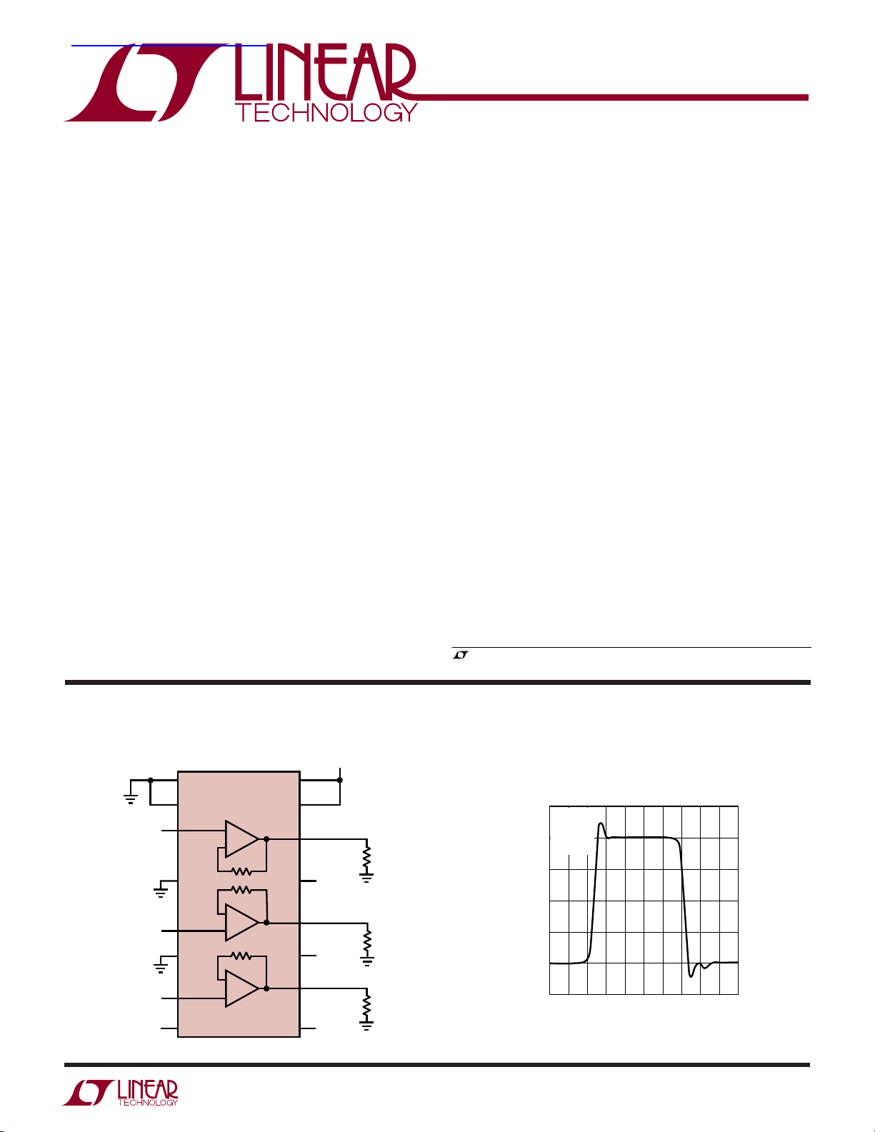
The LT®6554 is a high-speed triple video buffer with an
internally fixed gain of 1. The individual buffers are optimized for performance with a 1k load and feature a
2V
full signal bandwidth of 400MHz, making them ideal
P–P
for driving very high-resolution video signals. Separate
power supply pins for each amplifier boost channel separation to 90dB, allowing the LT6554 to excel in many highspeed applications.
While the performance of the LT6554 is optimized for dual
supply operation, it can also be used on a single supply as
low as 4.5V. Using dual 5V supplies, each amplifier draws
only 8mA. When disabled, the amplifiers draw less than
100µA and the outputs become high impedance. Further-
more, the amplifiers are capable of turning on in less than
50ns, making them suitable for multiplexing and portable
applications.
The LT6554 is manufactured on Linear Technology’s
proprietary low voltage complementary bipolar process
and is available in the 16-lead SSOP package that fits in the
same PCB area as an SO-8 package.
, LTC and LT are registered trademarks of Linear Technology Corporation.
All other trademarks are the property of their respective owners.
TYPICAL APPLICATIO
Triple Video Buffer and A/D Driver
LT6554
R
G
B
–5V
3
IN
4
5
IN
6
7
IN
8
+
–
480Ω
480Ω
–
+
480Ω
–
+
U
5V
161
152
14
1k
13
–5V
12
11
10
9
1k
5V
1k
–5V
6554 TA01a
Large Signal Transient Response
1.5
V
= 2V
OUT
P–P
VS = ±5V
= 1k
R
1.0
L
= 25°C
T
A
0.5
0
OUTPUT (V)
–0.5
–1.0
–1.5
4 8 12 16
TIME (ns)
2020 6 10 14 18
6554 TA01b
6554fa
1
LT6554
1
2
3
4
5
6
7
8
TOP VIEW
GN PACKAGE
16-LEAD PLASTIC SSOP
16
15
14
13
12
11
10
9
EN
DGND
INR
AGND
ING
AGND
INB
V
–
V
+
V
+
OUTR
V
–
OUTG
V
+
OUTB
V
–
G = +1
G = +1
G = +1
WW
W
ABSOLUTE AXI U RATI GS
U
UUW
PACKAGE/ORDER I FOR ATIO
(Note 1)
Total Supply Voltage (V+ to V–) ............................ 13.2V
Input Current (Note 2) ........................................ ±10mA
Output Current (Continuous) ............................. ±70mA
EN to DGND Voltage (Note 2) ................................. 5.5V
ORDER PART
NUMBER
LT6554CGN
LT6554IGN
Output Short-Circuit Duration (Note 3) ............ Indefinite
Operating Temperature Range (Note 4) ... –40°C to 85°C
Specified Temperature Range (Note 5) .... –40°C to 85°C
Storage Temperature Range ..................–65°C to 150°C
Junction Temperature........................................... 150°C
Lead Temperature (Soldering, 10 sec).................. 300°C
T
= 150°C, θJA = 135°C/W
JMAX
Consult LTC Marketing for parts specified with wider operating temperature ranges.
ELECTRICAL CHARACTERISTICS
temperature range, otherwise specifications are at TA = 25°C. VS = ±5V, RL = 1k, CL = 1.5pF, VEN = 0.4V, V
SYMBOL PARAMETER CONDITIONS MIN TYP MAX UNITS
V
OS
I
IN
e
n
i
n
R
IN
C
IN
PSRR Power Supply Rejection Ratio VS (Total) = 4.5V to 12V (Note 6) ● 51 65 dB
I
PSRR
AV ERR Gain Error V
AV MATCH Gain Matching Any One Channel to Another ±0.03 %
V
OUT
I
S
I
EN
I
SC
SR Slew Rate 4V
–3dB BW Small Signal –3dB Bandwidth V
0.1dB BW Gain Flatness ±0.1dB Bandwidth V
Offset Voltage VIN = 0V, VOS = V
Input Current ● –17 ±50 µA
Output Noise Voltage f = 100kHz 20 nV√Hz
Input Noise Current f = 100kHz 3.5 pA√Hz
Input Resistance VIN = ±1V ● 150 400 kΩ
Input Capacitance f = 100kHz 1 pF
Input Current Power Supply VS (Total) = 4.5V to 12V (Note 6) ● 1 ±5 µA/V
Rejection
Maximum Output Voltage Swing ● ±3.75 ±3.85 V
Supply Current, Per Amplifier RL = ∞ 810 mA
Supply Current, Disabled, Total VEN = 4V ● 22 100 µA
Enable Pin Current VEN = 0.4V ● –200 –95 µA
Output Short-Circuit Current RL = 0Ω, VIN = ±2V ● ±50 ±105 mA
The ● denotes the specifications which apply over the full operating
AGND
OUT
= ±2V ● –2.5 –0.6 0 %
OUT
= ∞ ● 13 mA
R
L
= Open ● 0.5 100 µA
V
EN
+
V
= V
EN
Output Step (Note 9) 1700 2500 V/µs
P-P
= 200mV
OUT
= 200mV
OUT
P-P
P-P
● ±70 mV
● 0.5 50 µA
GN PART
MARKING
6554
6554I
, V
= 0V.
DGND
11 ±35 mV
650 MHz
100 MHz
6554fa
2
LT6554
ELECTRICAL CHARACTERISTICS
temperature range, otherwise specifications are at T
The ● denotes the specifications which apply over the full operating
= 25°C. VS = ±5V, RL = 1k, CL = 1.5pF, VEN = 0.4V, V
A
AGND
, V
DGND
= 0V.
SYMBOL PARAMETER CONDITIONS MIN TYP MAX UNITS
LSBW Large Signal Bandwidth V
All-Hostile Crosstalk f = 10MHz, V
t
S
tR, t
F
Settling Time 0.1% of V
Small-Signal Rise and Fall Time 10% to 90%, V
= 2V
OUT
P-P
= 4V
V
OUT
P-P
f = 100MHz, V
FINAL
(Note 7) 270 400 MHz
(Note 7) 200 MHz
= 2V
OUT
P-P
= 2V
OUT
P-P
, V
= 2V 6 ns
STEP
= 200mV
OUT
P-P
–90 dB
–60 dB
550 ps
dG Differential Gain (Note 8) 0.022 %
dP Differential Phase (Note 8) 0.006 Deg
HD2 2nd Harmonic Distortion f = 10MHz, V
HD3 3rd Harmonic Distortion f = 10MHz, V
Note 1: Absolute Maximum Ratings are those values beyond which the life
of a device may be impaired.
Note 2: This parameter is guaranteed to meet specified performance
through design and characterization. It is not production tested.
Note 3: As long as output current and junction temperature are kept below
the Absolute Maximum Ratings, no damage to the part will occur.
Depending on the supply voltage, a heat sink may be required.
Note 4: The LT6554C is guaranteed functional over the operating
temperature range of –40°C to 85°C.
Note 5: The LT6554C is guaranteed to meet specified performance from
0°C to 70°C. The LT6554C is designed, characterized and expected to
meet specified performance from –40°C and 85°C but is not tested or QA
sampled at these temperatures. The LT6554I is guaranteed to meet
specified performance from –40°C to 85°C.
OUT
OUT
= 2V
= 2V
P-P
P-P
–82 dBc
–96 dBc
Note 6: The two supply voltage settings for power supply rejection are
shifted from the typical ±V
measurement is taken at V
points for ease of testing. The first
S
+
= 3V, V– = –1.5V to provide the required 3V
headroom for the enable circuitry to function with EN, DGND, AGND and
all inputs connected to 0V. The second measurement is taken at V+ = 8V,
–
= –4V.
V
Note 7: Large signal bandwidth is calculated from the slew rate:
LSBW = SR/(π • V
P-P
)
Note 8: Differential gain and phase are measured using a Tektronix
TSG120YC/NTSC signal generator and a Tektronix 1780R video
measurement set. The resolution of this equipment is better than 0.05%
and 0.05°. Nine identical amplifier stages were cascaded giving an
effective resolution of better than 0.0056% and 0.0056°.
Note 9: Slew rate is 100% production tested on the G channel. Slew rate
of the R and B channels is guaranteed through design and
characterization.
6554fa
3
LT6554
UW
TYPICAL PERFOR A CE CHARACTERISTICS
Supply Current per Amplifier vs
Temperature
12
10
8
6
4
SUPPLY CURRENT (mA)
2
0
–35 5
–55
15.0
VS = ±5V
V
IN
12.5
TYPICAL PART
10.0
7.5
5.0
2.5
OFFSET VOLTAGE (mV)
0
–2.5
–5.0
–35 5
–55
–15
= 0V
–15
VEN = 0V
VEN = 0.4V
45 125
25
TEMPERATURE (°C)
45 125
25
TEMPERATURE (°C)
Supply Current per Amplifier vs
Supply Voltage
VS = ±5V
= ∞
R
L
= 0V
V
IN
85
105
65
6554 G01
12
10
8
6
4
SUPPLY CURRENT (mA)
2
0
+
V– = –V
VEN, V
T
04
, VIN = 0V
DGND
= 25°C
A
123
56789101112
TOTAL SUPPLY VOLTAGE (V)
6554 G02
Supply Current per Amplifier vs
EN Pin Voltage
12
10
8
TA = 125°C
6
4
SUPPLY CURRENT (mA)
2
0
0
TA = –55°C
TA = 25°C
0.5 1.5
1.0
EN PIN VOLTAGE (V)
2.0
2.5
VS = ±5V
V
DGND
= 0V
V
IN
3.0
= 0V
3.5
6554 G03
4.0
Input Bias Current vs
Input Voltage
20
VS = ±5V
0
–20
–40
INPUT BIAS CURRENT (µA)
85
105
65
6554 G04
–60
–2.5
TA = 125°C
TA = 25°C
TA = –55°C
–1.5
–0.5
INPUT VOLTAGE (V)
0.5
1.5
2.5
6554 G05
–100
EN PIN CURRENT (µA)
–120
–140
–20
–40
–60
–80
0
0
EN Pin Current vs EN Pin VoltageOffset Voltage vs Temperature
VS = ±5V
V
= 0V
DGND
TA = 125°C
1
TA = –55°C
TA = 25°C
34
2
EN PIN VOLTAGE (V)
5
6554 G06
Output Voltage vs Input Voltage
5
VS = ±5V
4
= 1k
R
L
3
2
1
0
–1
TA = –55°C
–2
OUTPUT VOLTAGE (V)
–3
–4
–5
–3.5 –1.5
–4.5
TA = 125°C
–2.5
–0.5
INPUT VOLTAGE (V)
0.5 4.5
4
1.5
TA = 25°C
2.5
3.5
6554 G07
Output Voltage Swing vs I
(Output High)
5
VS = ±5V
= 4V
V
IN
4
TA = –55°C
3
2
OUTPUT VOLTAGE (V)
1
0
102030
0
40
SOURCE CURRENT (mA)
TA = 125°C
LOAD
TA = 25°C
6554 G08
Output Voltage Swing vs I
LOAD
(Output Low)
0
VS = ±5V
= –4V
V
IN
–1
–2
–3
TA = –55°C
OUTPUT VOLTAGE (V)
–4
–5
102030
10050 60 70 80 90
040
SINK CURRENT (mA)
TA = 25°C
TA = 125°C
10050 60 70 80 90
6554 G09
6554fa

UW
TYPICAL PERFOR A CE CHARACTERISTICS
LT6554
Input Noise Spectral Density Input Impedance vs Frequency PSRR vs Frequency
1000
100
10
INPUT NOISE (nV/√Hz OR pA/√Hz)
1
0.001 0.01 1 10 1000.1
Frequency Response
3
VS = ±5V
= 1k
R
2
L
= 1.5pF
C
L
1
= 25°C
T
A
0
–1
–2
–3
AMPLITUDE (dB)
–4
–5
–6
0.1
1 100
e
n
i
n
FREQUENCY (kHz)
V
OUT
V
= 2V
OUT
V
= 4V
OUT
10
FREQUENCY (MHz)
VS = ±5V
= 25°C
T
A
= 200mV
P-P
P-P
6554 G10
P-P
6554 G13
1000
1000
100
10
INPUT IMPEDANCE (kΩ)
1
0.1
0.01 0.1 10 100 10001
FREQUENCY (MHz)
Gain Flatness vs Frequency
0.5
VS = ±5V
= 200mV
V
0.4
OUT
RL = 1k
0.3
= 1.5pF
C
L
= 25°C
T
A
0.2
TYPICAL PART
0.1
0
– 0.1
AMPLITUDE (dB)
– 0.2
– 0.3
– 0.4
– 0.5
0.1 10 100 10001
P-P
G-CHANNEL
FREQUENCY (MHz)
R-CHANNEL
B-CHANNEL
VS = ±5V
= 0V
V
IN
= 25°C
T
A
6554 G11
6554 G14
70
±PSRR
60
+PSRR
50
–PSRR
40
30
20
REJECTION RATIO (dB)
10
0
0.001 0.01 1 10 1000.1
Crosstalk vs Frequency
0
VS = ±5V
= 2V
V
OUT
RL = 1k
–20
= 25°C
T
A
–40
–60
AMPLITUDE (dB)
–80
– 100
– 120
0.1
VS = ±5V
= 25°C
T
A
FREQUENCY (MHz)
P-P
ALL-
HOSTILE
1 10 100 1000
FREQUENCY (MHz)
6554 G12
WORST
ADJACENT
6554 G15
Frequency Response with
Capacitive Loads
12
VS = ±5V
= 200mV
V
10
OUT
RL = 1k
8
= 25°C
T
A
6
4
2
0
AMPLITUDE (dB)
–2
–4
–6
0.1
P-P
1 100
FREQUENCY (MHz)
CL = 9pF
CL = 6.8pF
CL = 3.3pF
10
CL = 12pF
CL = 1.5pF
6554 G16
1000
Harmonic Distortion vs Frequency Output Impedance vs Frequency
0
VS = ±5V
–10
–20
–30
–40
–50
–60
–70
–80
DISTORTION (dBc)
–90
–100
–110
–120
= 2V
V
OUT
RL = 1k
= 25°C
T
A
0.01 1 10 1000.1
P-P
HD2
HD3
FREQUENCY (MHz)
6554 G17
100000
10000
1000
100
OUTPUT IMPEDANCE (Ω)
0.1
DISABLED
= 4V
V
EN
10
1
0.01
0.1 1 10 100
ENABLED
= 0.4V
V
EN
FREQUENCY (MHz)
VS = ±5V
= 1k
R
L
= 25°C
T
A
6554 G18
6554fa
1000
5

LT6554
UW
TYPICAL PERFOR A CE CHARACTERISTICS
Maximum Capacitive Load vs
Output Series Resistor
35
30
25
20
15
10
OUTPUT SERIES RESISTANCE (Ω)
5
0
1
AC PEAKING
>2dB
10 100 1000
CAPACITIVE LOAD (pF)
1.5
1.0
0.5
0
OUTPUT (V)
–0.5
–1.0
–1.5
Small Signal Transient Response
0.15
V
= 2V
OUT
VS = ±5V
= 1k
R
L
= 25°C
T
A
P–P
VIN = 100mV
VS = ±5V
R
0.10
T
0.05
0
OUTPUT (V)
–0.05
–0.10
–0.15
= 1k
L
= 25°C
A
20 6 10 14 18
4 8 12 16 20
Large Signal Transient Response
VIN = 2V
P–P
VS = ±5V
= 1k
R
L
= 25°C
T
A
20 6 10 14 18
4 8 12 16 20
TIME (ns)
6554 G21
P–P
TIME (ns)
Video Amplitude Transient
Response
0.9
0.8
0.7
0.6
0.5
0.4
0.3
OUTPUT (V)
0.2
0.1
0
–0.1
6554 G196554 G25
Large Signal Transient Response
4
VIN = 5V
P–P
VS = ±5V
3
= 1k
R
L
= 25°C
T
A
2
1
0
OUTPUT (V)
–1
–2
–3
–4
4 8 12 16 20
20 6 10 14 18
TIME (ns)
VIN = 700mV
VS = ±5V
R
L
T
A
P–P
= 1k
= 25°C
4 8 12 16 20
20 6 10 14 18
TIME (ns)
6554 G22
6554 G20
6
Gain Error Distribution
35
VS = ±5V
= ±2V
V
OUT
30
= 1k
R
L
= 25°C
T
A
25
20
15
10
PERCENT OF UNITS (%)
5
0
–1.1 –0.9
GAIN ERROR–INDIVIDUAL CHANNEL (%)
–0.7
–0.5 –0.3
6554 G23
–0.1
Gain Error Matching Distribution
40
VS = ±5V
= ±2V
V
OUT
35
= 1k
R
L
= 25°C
T
A
30
25
20
15
PERCENT OF UNITS (%)
10
5
0
–0.10
–0.06
GAIN ERROR BETWEEN CHANNELS (%)
–0.02
0.02 0.06
0.10
6554 G24
6554fa

LT6554
U
UU
PI FU CTIO S
EN (Pin 1): Enable Control Pin. An internal pull-up resistor
of 46k defines the pin’s impedance and will turn the part off
if the pin is unconnected. When the pin is pulled low, the
part is enabled.
DGND (Pin 2): Digital Ground Reference for Enable Pin.
This pin is normally connected to ground.
INR (Pin 3): Red Channel Input. This pin has a nominal
impedance of 400kΩ and does not have any internal
termination resistor.
AGND (Pin 4): Analog Ground for Isolation Between Red
and Green Channel Inputs. The AGND pins have ESD
protection and therefore should not be connected to
potentials outside the power supply range.
ING (Pin 5): Green Channel Input. This pin has a nominal
impedance of 400kΩ and does not have any internal
termination resistor.
AGND (Pin 6): Analog Ground for Isolation Between Green
and Blue Channel Inputs. The AGND pins have ESD protection and therefore should not be connected to potentials
outside the power supply range.
INB (Pin 7): Blue Channel Input. This pin has a nominal
impedance of 400kΩ and does not have any internal
termination resistor.
V– (Pin 8): Negative Supply Voltage. V– pins are not
internally connected to each other, and must all be connected externally. Proper supply bypassing is necessary
for best performance. See the Applications Information
section.
V– (Pin 9): Negative Supply Voltage for Blue Channel
Output Stage. V– pins are not internally connected to each
other, and must all be connected externally. Proper supply
bypassing is necessary for best performance. See the
Applications Information section.
OUTB (Pin 10): Blue Channel Output. It is the buffered
output of the blue channel input.
V+ (Pin 11): Positive Supply Voltage for Blue and Green
Channel Output Stages. V+ pins are not internally connected to each other, and must all be connected externally.
Proper supply bypassing is necessary for best performance. See the Applications Information section.
OUTG (Pin 12): Green Channel Output. It is the buffered
output of the green channel input.
V– (Pin 13): Negative Supply Voltage for Green and Red
Channel Output Stages. V– pins are not internally connected to each other, and must all be connected externally.
Proper supply bypassing is necessary for best performance. See the Applications Information section.
OUTR (Pin 14): Red Channel Output. It is the buffered
output of the red channel input.
V+ (Pin 15): Positive Supply Voltage for Red Channel
Output Stage. V+ pins are not internally connected to each
other, and must all be connected externally. Proper supply
bypassing is necessary for best performance. See the
Applications Information section.
V+ (Pin 16): Positive Supply Voltage. V+ pins are not
internally connected to each other, and must all be connected externally. Proper supply bypassing is necessary
for best performance. See the Applications Information
section.
6554fa
7

LT6554
U
WUU
APPLICATIO S I FOR ATIO
Power Supplies
The LT6554 is optimized for ±5V supplies but can be
operated on as little as ±2.25V or a single 4.5V supply and
as much as ±6V or a single 12V supply. Internally, each
supply is independent to improve channel isolation. Do
not leave any supply pins disconnected!
Enable/Shutdown
The LT6554 has a TTL compatible shutdown mode controlled by the EN pin and referenced to the DGND pin. If the
amplifier will be enabled at all times, the EN pin can be
connected directly to DGND. If the enable function is
desired, either driving the pin above 2V or allowing the
internal 46k pull-up resistor to pull the EN pin to the top rail
will disable the amplifier. When disabled, the output will
become very high impedance. Supply current into the
amplifier in the disabled state will be primarily through V
and approximately equal to (V+ – VEN)/46k.
It is important that the two following constraints on the
DGND pin and the EN pin are always followed:
V+ – V
VEN – V
Split supplies of ±3V to ±5.5V will satisfy these require-
ments with DGND connected to 0V.
In single supply applications above 5.5V, an additional
resistor may be needed from the EN pin to DGND if the pin
is ever allowed to float. For example, on a 12V single
supply, a 33k resistor to ground would protect the pin from
floating too high while still allowing the internal pull-up
resistor to disable the part.
On dual ±2.25V supplies, connecting the EN and DGND
pins to V– is the easiest way of ensuring that V+ – V
is more than 3V.
The DGND pin should not be pulled above the EN pin since
doing so will turn on an ESD protection diode. If the EN pin
voltage is forced a diode drop below the DGND pin, current
should be limited to 10mA or less.
The enable/disable times of the LT6554 are fast when
driven with a logic input. Turn on (from 50% EN input to
50% output) typically occurs in less than 50ns. Turn off is
slower, but is nonetheless below 300ns.
DGND
DGND
≥ 3V
≤ 5.5V
+
DGND
Input Considerations
The LT6554 input voltage range is from V– + 1V to V+ – 1V
and is therefore larger than the output swing. The inputs
can be driven beyond the point at which the output clips so
long as input currents are limited to below ±10mA.
Layout and Grounding
It is imperative that care is taken in PCB layout in order to
utilize the very high speed and very low crosstalk of the
LT6554. Separate power and ground planes are highly
recommended and trace lengths should be kept as short
as possible. If input traces must be run over a distance of
several centimeters, they should use a controlled impedance with either series or shunt terminations (nominally
50Ω or 75Ω) to maintain signal fidelity.
Care should be taken to minimize capacitance on the
LT6554’s output traces by increasing spacing between
traces and adjacent metal and by eliminating metal planes
in underlying layers. To drive cable or traces longer than
several centimeters, using the LT6553 with its fixed gain
of +2 in conjunction with series and load termination
resistors may provide better results.
A plot of LT6554 performance driving a 1k load with
various trace lengths is shown in Figure 1. All data is from
a 4-layer board with 2oz copper, 18mil of board layer
thickness to the ground plane, a trace width of 12mils and
spacing to adjacent metal of 18mils. The 0.2cm output
trace places the 1k resistor as close to the part as possible,
while the other curves show the load resistor consecutively further away. The worst case, 4cm, trace has almost
10pF of parasitic capacitance.
In order to counteract any peaking in the frequency response from driving a capacitive load, a series resistance
can be inserted in the line at the output of the part to flatten
the response. Figure 2 shows the frequency response with
the same 4cm trace from Figure 1, now with a 10Ω series
resistor inserted near the output pin of the LT6554. Note
that using a 10Ω series resistor with a 1k load only
decreases the output amplitude by 0.1dB or 1% and has a
minimal effect on the bandwidth of the system. See the
graph labeled “Maximum Capacitive Load vs Output Series Resistor” in the Typical Performance Characteristics
section for more information.
8
6554fa

WUUU
APPLICATIO S I FOR ATIO
6
VS = ±5V
= 200mV
V
OUT
RL = 1k
4
= 25°C
T
A
2
0
AMPLITUDE (dB)
–2
–4
P-P
4cm TRACE
2cm TRACE
0.2cm TRACE
LT6554
supply. The smallest value capacitors should be placed
closest to the package.
To maintain the LT6554’s channel isolation, it is beneficial
to shield parallel input and output traces using a ground
plane or power supply traces. Vias between topside and
backside metal are recommended to maintain a low
inductance ground, especially between closely spaced
signal traces.
–6
0.1
1
10 100 1000
FREQUENCY (MHz)
6554 F01
Figure 1. Response vs Output Trace Length
6
VS = ±5V
= 200mV
V
OUT
RL = 1k
4
= 25°C
T
A
2
0
AMPLITUDE (dB)
–2
–4
–6
0.1
P-P
1
10 100 1000
FREQUENCY (MHz)
4cm TRACE
4cm TRACE
R
S, OUT
= 10Ω
6554 F02
Figure 2. Response vs Series Output Resistance
While the AGND pins on the LT6554 are not connected to
the amplifier circuitry, tying them to ground or another
“quiet” node significantly increases channel isolation and
is always recommended. The AGND pins do have ESD
protection and therefore should not be connected to
potentials outside the power supply range.
Single Supply Operation
Figure 3 illustrates how to use the LT6554 with a single
supply ranging from 4.5V to 12V. Since the output range
is comparable to the input range, the DC bias point at the
input can be set anywhere between the supplies that will
prevent the AC-coupled signal from running into the
output range limits. As shown, the DC input level is midsupply.
The only additional power dissipation in the single supply
configuration is through the resistor bias string at the
input and through any load resistance at the output. In
many cases, the output can be used to directly drive other
single supply devices without additional coupling and
without any resistive load.
ESD Protection
The LT6554 has reverse-biased ESD protection diodes on
all pins. If any pins are forced a diode drop above the
positive supply or a diode drop below the negative supply,
large currents may flow through these diodes. If the
current is kept below 10mA, no damage to the device will
occur.
4.5V TO 12V
Low ESL/ESR bypass capacitors should be placed as close
to the positive and negative supply pins as possible. One
4700pF ceramic capacitor is recommended for both V
+
and V–. Additional 470pF ceramic capacitors with minimal
trace length on each supply pin will further improve AC and
transient response as well as channel isolation. For high
current drive and large-signal transient applications, additional 1µF to 10µF tantalums should be added on each
22µF
V
IN
5k
IN
AGND
5k
1/3
LT6554
+
V
OUT
–
V
6554 F03
Figure 3. Single Supply Configuration, One Channel Shown
6554fa
9

LT6554
TYPICAL APPLICATIO
U
RGB Buffer Demo Board
The DC794 Demo Board illustrates optimal routing,
bypassing and termination using the LT6554 as an
RGB video buffer. The schematic is shown in Figure 4. All
inputs and outputs are routed to have a characteristic
impedance of 75Ω. The 75Ω input shunt and output series
terminations are connected as close to the part as possible. While the 75Ω back termination resistors at the
outputs of the LT6554 minimize signal reflections in the
output traces and isolate the part from any capacitive
loading in those traces, they also contribute to gain error
if the output is not terminated with high impedance. For
example, if the output is terminated with a 1k load, the 75Ω
back termination will cause a 7% gain error. Decreasing
the value of the back termination resistors will decrease
the signal attenuation but may compromise the AC response. However, connecting the LT6554 outputs to the
output traces on the DC794 board without some series
resistance is not recommended; 10Ω to 20Ω is generally
sufficient.
A fourth signal trace is provided at the bottom of the
DC794 demo board with dimensions identical to the
E1
EN
R4
75Ω
JP3
JP1
CONTROL
31
2
ENABLE EXT
31
E2
DGND
R6
R5
75Ω
75Ω
DUALSINGLE
2
C5
470pF
C6
1000pFC7470pFC84700pFC910µF, 16V
LT6554
1
EN
2
DGND
3
INR
4
AGND
5
ING
6
AGND
7
INB
8
–
V
OUTR
OUTG
OUTB
Figure 4. DC794 Demo Board Schematic
INR
ING
CAL
INB
5
4
3
2
5
4
3
2
5
4
3
2
AGND
5
4
3
2
J1
50Ω BNC
1
EN
5432
BNC × 3
J5
J6
J7
J3
BANANA
JACK
J8
BNC
1
Z = 75
Z = 75
1
Z = 75
1
AGND
1
JP2
DGND
2
AGND FLOAT
E3
13
SUPPLY
combined input and output of the other channels. This
trace can be used for calibrating the effects of electrical
delay and impedance mismatching and is not necessary
in an end-user application. Jumpers and additional connectors are also included to allow for evaluation of the
enable feature and single supply operation.
RGB Video Selector/Cable Driver
A video multiplexer can be implemented using the EN pins
of parallel LT6554s as shown in Figure 5. In this application, the corresponding outputs are connected together
and one LT6554 is switched on while the other is switched
off. A fast inverter provides a complementary signal to
ensure that only one set of R, G and B channels is buffered
at any time.
Since the output impedance of a disabled LT6554 is very
high, adding additional channels will not resistively load
an enabled output. However, since the disabled LT6554
has around 6pF of capacitance, it may be desirable to
resistively isolate the outputs of each channel to maintain
flat frequency response as shown in the graph labeled
“Maximum Capacitive Load vs Output Series Resistor” in
the Typical Performance Characteristics section.
+
V
+
C1
4700pF
16
+
V
15
+
V
14
13
–
V
12
11
+
V
10
9
–
V
1210
C2
470pFC34700pFC410µF, 16V
R1
75Ω
R2
75Ω
R3
75Ω
ALL BNC: CANARE BCJ-BPLH
1210
Z = 75
Z = 75
Z = 75
Z = 75
V
J2
BANANA
JACK
BNC x3
1
J9
1
J10
1
J11
–
V
V
J4
BANANA JACK
1
J12
BNC
5
4
OUTR
3
2
5
4
OUTG
3
2
5
4
OUTB
3
2
–
5
4
CAL
3
2
6554 F04
6554fa
10

WW
SI PLIFIED SCHE ATIC
LT6554
+
V
BIAS
46k
1k
EN
DGND
–
V
PACKAGE DESCRIPTIO
TO OTHER
AMPLIFIERS
+
V
150Ω
IN
–
V
U
GN Package
16-Lead Plastic SSOP (Narrow .150 Inch)
(Reference LTC DWG # 05-08-1641)
.045 ±.005
16
.189 – .196*
(4.801 – 4.978)
15
14
13
12 11 10
+
V
480Ω
OUT
–
V
6554 SS
.009
(0.229)
9
REF
.254 MIN
RECOMMENDED SOLDER PAD LAYOUT
.007 – .0098
(0.178 – 0.249)
.016 – .050
NOTE:
1. CONTROLLING DIMENSION: INCHES
2. DIMENSIONS ARE IN
3. DRAWING NOT TO SCALE
*DIMENSION DOES NOT INCLUDE MOLD FLASH. MOLD FLASH
SHALL NOT EXCEED 0.006" (0.152mm) PER SIDE
**DIMENSION DOES NOT INCLUDE INTERLEAD FLASH. INTERLEAD
FLASH SHALL NOT EXCEED 0.010" (0.254mm) PER SIDE
(0.406 – 1.270)
INCHES
(MILLIMETERS)
Information furnished by Linear Technology Corporation is believed to be accurate and reliable.
However, no responsibility is assumed for its use. Linear Technology Corporation makes no representation that the interconnection of its circuits as described herein will not infringe on existing patent rights.
.150 – .165
.0250 TYP.0165 ± .0015
.015 ± .004
(0.38 ± 0.10)
0° – 8° TYP
× 45°
.229 – .244
(5.817 – 6.198)
.053 – .068
(1.351 – 1.727)
.008 – .012
(0.203 – 0.305)
12
.150 – .157**
(3.810 – 3.988)
5
4
3
678
.004 – .0098
(0.102 – 0.249)
.0250
(0.635)
BSC
GN16 (SSOP) 0502
6554fa
11

LT6554
TYPICAL APPLICATIO
U
3.3V
SEL
NC7SZ14
R
1
G
1
B
1
75Ω
75Ω
75Ω
R
0
G
0
B
0
75Ω
75Ω
75Ω
1
LT6554
2
3
×1
4
5
×1
6
7
×1
8
1
LT6554
2
3
×1
4
5
×1
6
7
×1
8
16
15
14
13
12
11
10
9
R
G
16
15
14
13
12
11
10
9
NOTE:
POWER SUPPLY BYPASS
CAPACITORS NOT SHOWN FOR CLARITY
B
OUT
OUT
OUT
–3.3V
6554 F05
Figure 5. RGB Video Selector and A/D Driver
RELATED PARTS
PART NUMBER DESCRIPTION COMMENTS
LT1259/LT1260 Dual/Triple 130MHz Current Feedback Amplifiers Shutdown, Operates to ±15V
LT1395/LT1396/LT1397 Single/Dual/Quad 400MHz Current Feedback Amplifiers 800V/µs Slew Rate
LT1398/LT1399 Dual/Triple 300MHz Current Feedback Amplifiers 0.1dB Gain Flatness to 150MHz, Shutdown
LT1675/LT1675-1 250MHz, Triple and Single RGB Multiplexer with 100MHz Pixel Switching, –3dB Bandwidth: 250MHz,
Current Feedback Amplifiers 1100V/µs Slew Rate
LT1809/LT1810 Single/Dual, 180MHz, Rail-to-Rail Input and 350V/µs Slew Rate, Shutdown,
Output Amplifiers Low Distortion –90dBc at 5MHz
LT6550/LT6551 3.3V Triple and Quad Video Buffers 110MHz Gain of 2 Buffers in MSOP Package
LT6553 650MHz, Gain of 2, Triple Video Amplifier Same Pinout as LT6554
6554fa
LT/TP 0305 1K REV A • PRINTED IN USA
© LINEAR TECHNOLOGY CORPORATION 2004
12
Linear Technology Corporation
1630 McCarthy Blvd., Milpitas, CA 95035-7417
(408) 432-1900 ● FAX: (408) 434-0507
●
www.linear.com
 Loading...