

Linear Technology LT6552IS8, LT6552IDD, LT6552CS8, LT6552CDD Datasheet
LT6552
Final Electrical Specifications
3.3V Single Supply
Video Difference Amplifier
FEATURES
■
Differential or Single-Ended Gain Block
■
Wide Supply Range 3V to 12.6V
■
Output Swings Rail-to-Rail
■
Input Common Mode Range Includes Ground
■
600V/µs Slew Rate
■
–3dB Bandwidth = 75MHz, AV = ±2
■
CMRR at 10MHz: >60dB
■
Output Swings Rail-to-Rail
■
Specified on 3.3V, 5V and ±5V Supplies
■
High Output Drive: ±70mA
■
Power Shutdown to 300µA
■
Operating Temperature Range: –40°C to 85°C
■
Tiny 3mm x 3mm x 1mm DFN Package
U
APPLICATIO S
■
Differential to Single-Ended Conversion
■
Video Line Driver
■
Automotive Displays
■
RGB Amplifiers
■
Coaxial Cable Drivers
■
Low Voltage High Speed Signal Processing
U
July 2003
DESCRIPTIO
The LT®6552 is a video difference amplifier optimized for
low voltage single supply operation. This versatile amplifier features uncommitted high input impedance (+) and
(–) inputs and can be used in differential or single-ended
configurations. A second set of inputs gives gain adjustment and DC control to the differential amplifier.
On a single 3.3V supply, the input voltage range extends
from ground to 1.3V and the output can swing to within
400mV of the supply voltage while driving a 150Ω load.
The LT6552 features 75MHz – 3dB bandwidth, 600V/µs
slew rate, and ±70mA output current making it ideal for
driving cables directly. The LT6552 maintains its performance for supplies from 3V to 12.6V and is fully specified
at 3.3V, 5V and ±5V supplies. The shutdown feature
reduces power dissipation to less than 1mW and allows
multiple amplifiers to drive the same cable.
The LT6552 is available in the 8-pin SO package as well as
a tiny, dual fine pitch leadless package (DFN). The device
is specified over the commercial and industrial temperature range.
, LTC and LT are registered trademarks of Linear Technology Corporation.
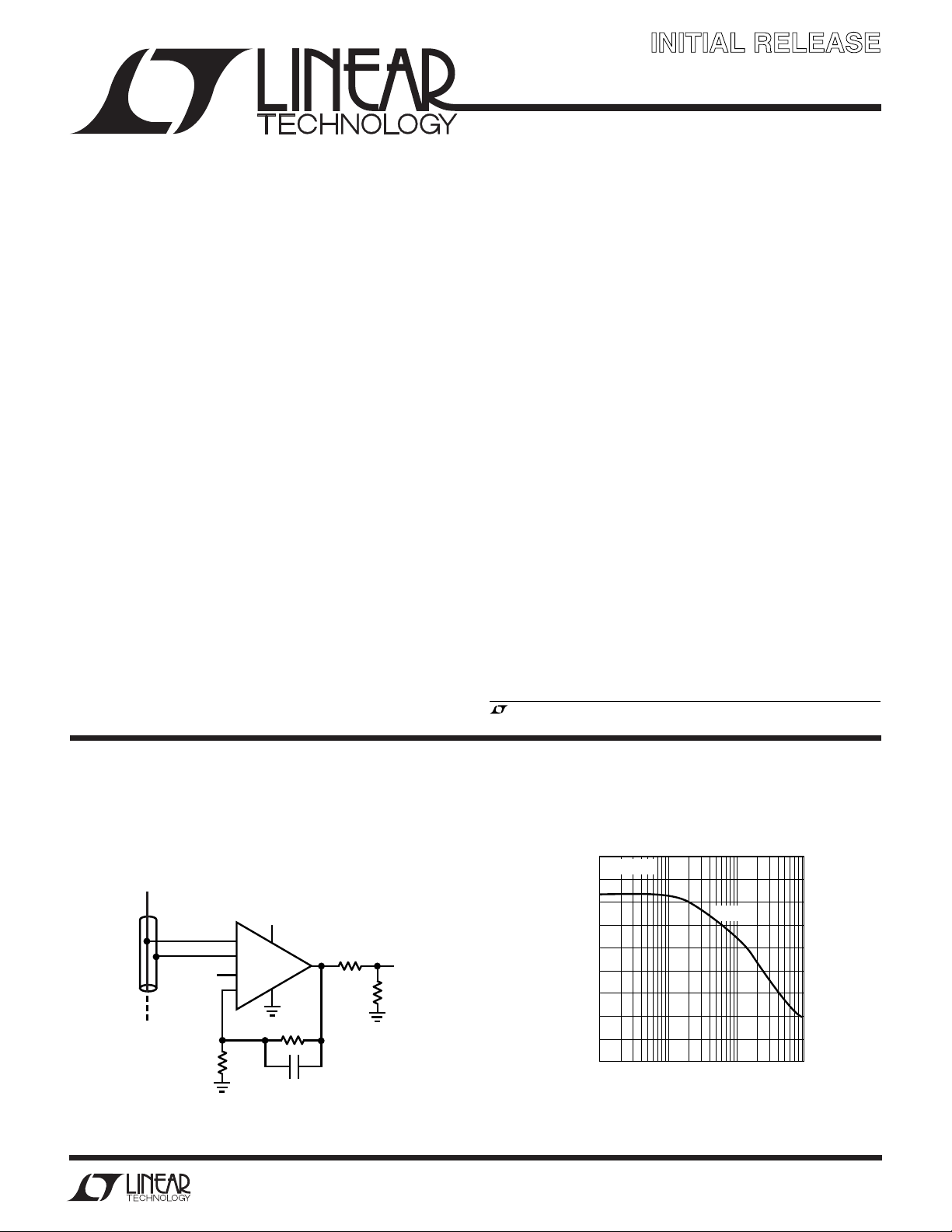
TYPICAL APPLICATIO
Cable Sense Amplifier for Loop Through
Connections with DC Adjust
V
IN
3
500Ω
2
1
8
R
G
CABLE
V
= 0.25V
DC
U
Input Referred CMRR vs Frequency
100
VS = 5V, 0V
90
5V
7
+
–
LT6552
REF
FB
4
R
500Ω
C
8pF
Information furnished by Linear Technology Corporation is believed to be accurate and reliable.
However, no responsibility is assumed for its use. Linear Technology Corporation makes no representation that the interconnection of its circuits as described herein will not infringe on existing patent rights.
75Ω
6
F
F
V
75Ω
6552 TA01a
OUT
80
70
60
50
40
30
20
COMMON MODE REJECTION RATIO (dB)
10
100k
VCM = 0V
1 10 100
FREQUENCY (MHz)
6552 TA01b
6552i
1
LT6552
WW
W
ABSOLUTE AXI U RATI GS
U
(Note 1)
Supply Voltage (V+ to V–) .................................... 12.6V
Input Current (Note 2) ........................................ ±10mA
Input Voltage Range .................................................±V
Differential Input Voltage
+Input (Pin 3) to –Input (Pin 2)................................±V
Output Short-Circuit Duration (Note 3)............ Indefinite
UUW
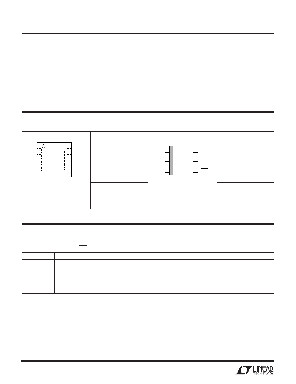
PACKAGE/ORDER I FOR ATIO
TOP VIEW
FB
1REF
–IN
2
+IN
3
–
V
4
8-LEAD (3mm × 3mm) PLASTIC DFN
T
DD PACKAGE
= 125°C, θJA = 160°C/W (NOTE 3)
JMAX
UNDERSIDE METAL INTERNALLY
CONNECTED TO V
(PCB CONNECTION OPTIONAL)
8
+
V
7
OUT
6
SHDN
5
–
ORDER PART
NUMBER
LT6552CDD
LT6552IDD
DD PART MARKING*
ADR
Operating Temperature Range (Note 4) ...–40°C to 85°C
Specified Temperature Range (Note 5)....–40°C to 85°C
Maximum Junction Temperature .......................... 150°C
S
(DD Package) ................................................... 125°C
Storage Temperature Range ..................–65°C to 150°C
S
(DD Package) ....................................–65°C to 125°C
Lead Temperature (Soldering, 10 sec).................. 300°C
ORDER PART
TOP VIEW
REF
1
–IN
2
+IN
3
–
V
4
S8 PACKAGE
8-LEAD PLASTIC SO
T
= 150°C, θJA = 100°C/W
JMAX
FB
8
+
V
7
OUT
6
SHDN
5
NUMBER
LT6552CS8
LT6552IS8
S8 PART MARKING
6552
6552I
*The temperature grade is identified by a label on the shipping container. Consult LTC Marketing for parts specified with wider operating temperature ranges.
3.3V ELECTRICAL CHARACTERISTICS
The ● denotes the specifications which apply over the full
operating temperature range, otherwise specifications are at TA = 25°C. VS = 3.3V, 0V. Figure 1 shows the DC test circuit,
V
= VCM = 1V, V
REF
SYMBOL PARAMETER CONDITIONS MIN TYP MAX UNITS
V
OS
∆VOS/∆T Input VOS Drift ● 40 µV/°C
I
B
I
OS
= 0V, V
DIFF
Input Offset Voltage Both Inputs (Note 7) 5 20 mV
Input Bias Current Any Input ● 25 50 µA
Input Offset Current Either Input Pair ● 15 µA
= V+, unless otherwise noted. RL = RF + RG = 1k. (Note 6)
SHDN
● 25 mV
2
6552i
LT6552
3.3V ELECTRICAL CHARACTERISTICS
The ● denotes the specifications which apply over the full
operating temperature range, otherwise specifications are at TA = 25°C. VS = 3.3V, 0V. Figure 1 shows the DC test circuit,
V
= VCM = 1V, V
REF
SYMBOL PARAMETER CONDITIONS MIN TYP MAX UNITS
e
n
i
n
R
IN
CMRR Common Mode Rejection Ratio VCM = 0V to 1.3V ● 58 75 dB
PSRR Power Supply Rejection VS = 3V to 12V ● 48 54 dB
G
E
V
OH
V
OL
SR Slew Rate V
FPBW Full-Power Bandwidth (Note 9) VO = 2V
BW Small-Signal –3dB Bandwidth AV = 2, RL = 150Ω 65 MHz
tr, t
f
t
S
I
SC
I
S
V
L
V
H
t
ON
t
OFF
DIFF
= 0V, V
= V+, unless otherwise noted. RL = RF + RG = 1k. (Note 6)
SHDN
Input Noise Voltage Density f = 10kHz 55 nV/√Hz
Input Noise Current Density f = 10kHz 0.7 pA/√Hz
Input Resistance Common Mode, VCM = 0V to 1.3V 300 kΩ
Input Range ● 0 1.3 V
Minimum Supply (Note 8) ● 3V
Gain Error VO = 0.5V to 2V, RL = 1k ● 13 %
= 150Ω ● 13 %
R
L
Swing High (V
Swing Low (V
= 0.4V), V
DIFF
= 1k ● 3.1 3.2 V
R
L
R
= 150Ω ● 2.5 2.9 V
L
= 75Ω 2 2.5 V
R
L
= –0.1V), V
DIFF
= 1k ● 850 mV
R
L
= 5mA ● 65 120 mV
I
SINK
I
= 10mA ● 40 200 mV
SINK
= 0.5V to 2.5V Measure from 1V to 2V, 350 V/µs
OUT
= 150Ω, AV = 2
R
L
P-P
(Pin 1) = 0V, AV = 10
REF
(Pin 1) = 0V, AV = 10
REF
55 MHz
Rise Time, Fall Time (Note 10) AV =50, VO = 0.5V to 2.5V, 125 175 ns
20% to 80%, R
Settling Time to 3% AV = 2, ∆V
Settling Time to 1% R
= 150Ω 30 ns
L
= 150Ω
L
= 2V 20 ns
OUT
Differential Gain AV = 2, RL = 150Ω, Black Level = 0.6V 0.4 %
Differential Phase AV = 2, RL = 150Ω, Black Level = 0.6V 0.15 Deg
Short-Circuit Current V
OUT
= 0V, V
= 1V 35 50 mA
DIFF
● 25 mA
Supply Current 12 13.5 mA
● 15 mA
Supply Current Shutdown V
= 0.5V ● 300 750 µA
SHDN
Shutdown Pin Input Low Voltage ● 0.5 V
Shutdown Pin Input High Voltage ● 3V
Shutdown Pin Current V
Turn On-Time V
Turn Off-Time V
= 0.5V ● 40 150 µA
SHDN
V
= 3V ● 310 µA
SHDN
from 0.5V to 3V 250 ns
SHDN
from 3V to 0.5V 450 ns
SHDN
6552i
3
 Loading...