

FEATURES
LT6552
3.3V Single Supply
Video Difference Amplifier
U
DESCRIPTIO
■
Differential or Single-Ended Gain Block
■
Wide Supply Range 3V to 12.6V
■
Output Swings Rail-to-Rail
■
Input Common Mode Range Includes Ground
■
600V/µs Slew Rate
■
–3dB Bandwidth = 75MHz, A
■
CMRR at 10MHz: >60dB
■
Specified on 3.3V, 5V and ±5V Supplies
■
High Output Drive: ±70mA
■
Power Shutdown to 300µA
■
Operating Temperature Range: –40°C to 85°C
■
Available in 8-Lead SO and
= ±2
V
Tiny 3mm x 3mm x 0.8mm DFN Packages
U
APPLICATIO S
■
Differential to Single-Ended Conversion
■
Video Line Driver
■
Automotive Displays
■
RGB Amplifiers
■
Coaxial Cable Drivers
■
Low Voltage High Speed Signal Processing
The LT®6552 is a video difference amplifier optimized for
low voltage single supply operation. This versatile amplifier features uncommitted high input impedance (+) and
(–) inputs and can be used in differential or single-ended
configurations. A second set of inputs gives gain adjustment and DC control to the differential amplifier.
On a single 3.3V supply, the input voltage range extends
from ground to 1.3V and the output swings from ground
to 2.9V while driving a 150Ω load. The LT6552 features
75MHz – 3dB bandwidth, 600V/µs slew rate, and ±70mA
output current making it ideal for driving cables directly.
The LT6552 maintains its performance for supplies from
3V to 12.6V and is fully specified at 3.3V, 5V and ±5V
supplies. The shutdown feature reduces power dissipation to less than 1mW and allows multiple amplifiers to
drive the same cable.
The LT6552 is available in the 8-lead SO package as well
as a tiny, dual fine pitch leadless package (DFN). The
device is specified over the commercial and industrial
temperature ranges.
, LTC and LT are registered trademarks of Linear Technology Corporation.
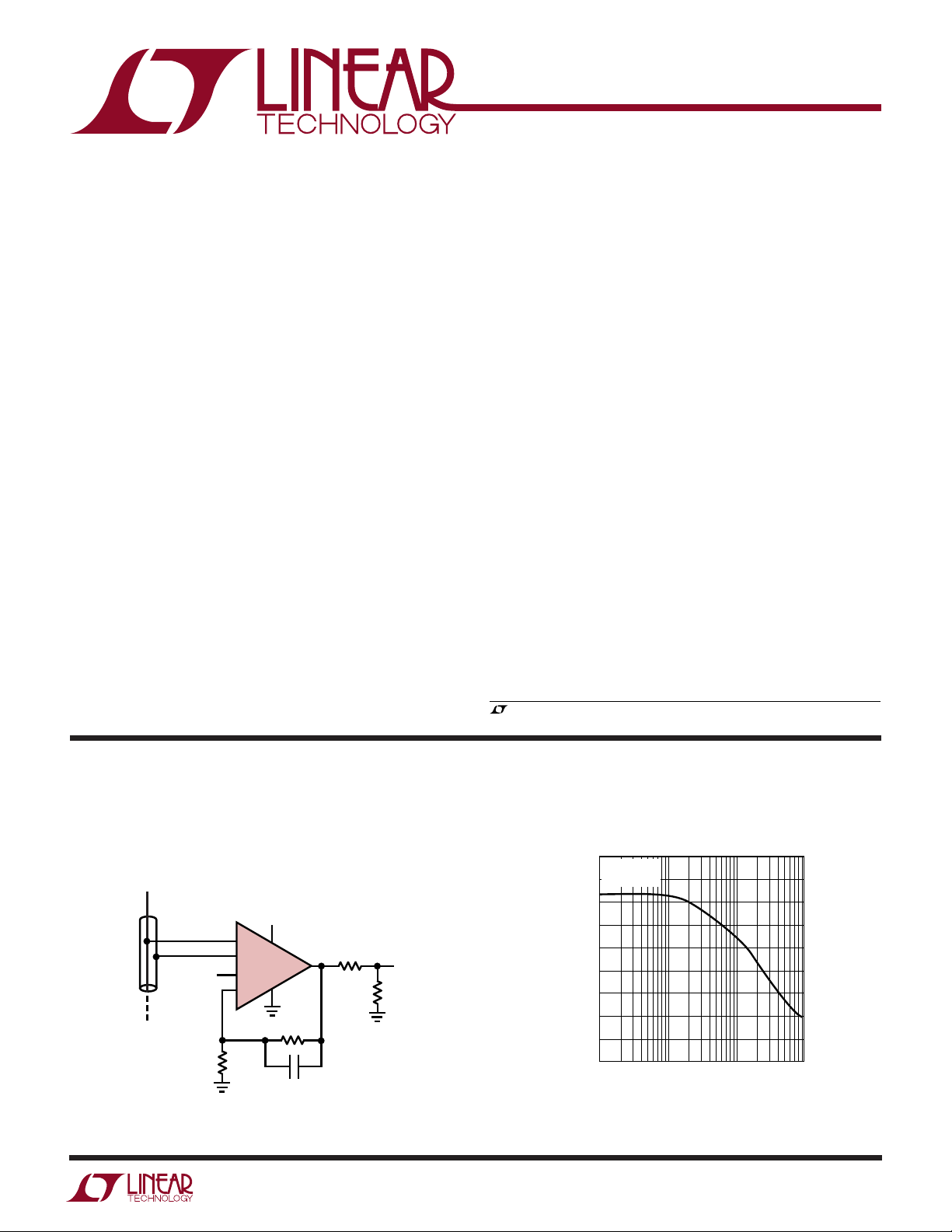
TYPICAL APPLICATIO
Cable Sense Amplifier for Loop Through
Connections with DC Adjust
V
IN
5V
CABLE
V
500Ω
3
2
1
DC
8
R
G
+
–
REF
FB
LT6552
7
4
500Ω
R
C
8pF
F
U
Input Referred CMRR vs Frequency
100
VS = 5V, 0V
= 0V DC
V
90
CM
80
70
75Ω
6
F
V
75Ω
6552 TA01a
OUT
60
50
40
30
20
COMMON MODE REJECTION RATIO (dB)
10
100k
1 10 100
FREQUENCY (MHz)
6552 TA01b
6552f
1
LT6552
WW
W
ABSOLUTE AXI U RATI GS
U
(Note 1)
Supply Voltage (V+ to V–) .................................... 12.6V
Input Current (Note 2) ........................................ ±10mA
Input Voltage Range ......................................... V– to V
Differential Input Voltage
+Input (Pin 3) to –Input (Pin 2)................................±V
Output Short-Circuit Duration (Note 3)............ Indefinite
Operating Temperature Range (Note 4) ...–40°C to 85°C
UUW
PACKAGE/ORDER I FOR ATIO
TOP VIEW
FB
1REF
–IN
2
+IN
3
–
V
4
8-LEAD (3mm × 3mm) PLASTIC DFN
UNDERSIDE METAL CONNECTED TO V
DD PACKAGE
T
= 125°C, θJA = 160°C/W
JMAX
(PCB CONNECTION OPTIONAL)
8
+
V
7
OUT
6
SHDN
5
–
ORDER PART
NUMBER
LT6552CDD
LT6552IDD
DD PART MARKING*
LADR
Specified Temperature Range (Note 5)....–40°C to 85°C
Maximum Junction Temperature .......................... 150°C
+
(DD Package) ................................................... 125°C
Storage Temperature Range ..................–65°C to 150°C
S
(DD Package) ....................................–65°C to 125°C
Lead Temperature
(Soldering, 10 sec) ........................................... 300°C
ORDER PART
TOP VIEW
REF
1
–IN
2
+IN
3
–
V
4
S8 PACKAGE
8-LEAD PLASTIC SO
T
= 150°C, θJA = 100°C/W
JMAX
FB
8
+
V
7
OUT
6
SHDN
5
NUMBER
LT6552CS8
LT6552IS8
S8 PART MARKING
6552
6552I
*The temperature grade is identified by a label on the shipping container. Consult LTC Marketing for parts specified with wider operating temperature ranges.
3.3V ELECTRICAL CHARACTERISTICS
The ● denotes the specifications which apply over the full
operating temperature range, otherwise specifications are at TA = 25°C. VS = 3.3V, 0V. Figure 1 shows the DC test circuit,
V
= VCM = 1V, V
REF
SYMBOL PARAMETER CONDITIONS MIN TYP MAX UNITS
V
OS
∆VOS/∆T Input VOS Drift ● 40 µV/°C
I
B
I
OS
= 0V, V
DIFF
Input Offset Voltage Both Inputs (Note 7) 5 20 mV
Input Bias Current Any Input ● 20 50 µA
Input Offset Current Either Input Pair ● 15 µA
= V+, unless otherwise noted. RL = RF + RG = 1k. (Note 6)
SHDN
● 25 mV
2
6552f
LT6552
3.3V ELECTRICAL CHARACTERISTICS
The ● denotes the specifications which apply over the full
operating temperature range, otherwise specifications are at TA = 25°C. VS = 3.3V, 0V. Figure 1 shows the DC test circuit,
V
= VCM = 1V, V
REF
SYMBOL PARAMETER CONDITIONS MIN TYP MAX UNITS
e
n
i
n
R
IN
CMRR Common Mode Rejection Ratio VCM = 0V to 1.3V ● 58 83 dB
PSRR Power Supply Rejection VS = 3V to 12V ● 48 54 dB
G
E
V
OH
V
OL
SR Slew Rate V
FPBW Full-Power Bandwidth (Note 9) VO = 2V
BW Small-Signal –3dB Bandwidth AV = 2, RL = 150Ω 65 MHz
tr, t
f
t
S
I
SC
I
S
V
L
V
H
t
ON
t
OFF
DIFF
= 0V, V
= V+, unless otherwise noted. RL = RF + RG = 1k. (Note 6)
SHDN
Input Noise Voltage Density f = 10kHz 55 nV/√Hz
Input Noise Current Density f = 10kHz 0.7 pA/√Hz
Input Resistance Common Mode, VCM = 0V to 1.3V 300 kΩ
Input Range ● 0 1.3 V
Minimum Supply (Note 8) ● 3V
Gain Error VO = 0.5V to 2V, RL = 1k ● 13 %
= 150Ω ● 13 %
R
L
Swing High (V
Swing Low (V
= 0.4V), V
DIFF
= 1k ● 3.1 3.2 V
R
L
R
= 150Ω ● 2.5 2.9 V
L
= 75Ω 2 2.5 V
R
L
= –0.1V), V
DIFF
= 1k ● 850 mV
R
L
= 5mA ● 65 120 mV
I
SINK
I
= 10mA ● 40 200 mV
SINK
= 0.5V to 2.5V Measure from 1V to 2V, 350 V/µs
OUT
= 150Ω, AV = 2
R
L
P-P
(Pin 1) = 0V, AV = 10
REF
(Pin 1) = 0V, AV = 10
REF
55 MHz
Rise Time, Fall Time (Note 10) AV =50, VO = 0.5V to 2.5V, 125 175 ns
20% to 80%, R
Settling Time to 3% AV = 2, ∆V
Settling Time to 1% R
= 150Ω 30 ns
L
= 150Ω
L
= 2V, Positive Step 20 ns
OUT
Differential Gain AV = 2, RL = 150Ω, Output Black Level = 0.6V 0.4 %
Differential Phase AV = 2, RL = 150Ω, Output Black Level = 0.6V 0.15 Deg
Short-Circuit Current V
OUT
= 0V, V
= 1V 35 50 mA
DIFF
● 25 mA
Supply Current 12.5 13.5 mA
● 15 mA
Supply Current, Shutdown V
= 0.5V ● 300 750 µA
SHDN
Shutdown Pin Input Low Voltage ● 0.5 V
Shutdown Pin Input High Voltage ● 3V
Shutdown Pin Current V
Turn On-Time V
Turn Off-Time V
Shutdown Output Leakage Current V
= 0.5V ● 40 150 µA
SHDN
V
= 3V ● 310 µA
SHDN
from 0.5V to 3V 250 ns
SHDN
from 3V to 0.5V 450 ns
SHDN
= 0.5V, 0V ≤ V
SHDN
OUT
≤ V
+
● 0.25 µA
6552f
3
LT6552
5V ELECTRICAL CHARACTERISTICS
The ● denotes the specifications which apply over the full operating
temperature range, otherwise specifications are at TA = 25°C. VS = 5V, 0V; Figure 1 shows the DC test circuit,
V
= VCM = 1V, V
REF
SYMBOL PARAMETER CONDITIONS MIN TYP MAX UNITS
V
OS
∆VOS/∆T Input VOS Drift ● 40 µV/°C
I
B
I
OS
e
n
i
n
R
IN
CMRR Common Mode Rejection Ratio VCM = 0V to 3V ● 58 83 dB
PSRR Power Supply Rejection VS = 3V to 12V ● 48 54 dB
G
E
V
OH
V
OL
SR Slew Rate V
FPBW Full-Power Bandwidth (Note 9) VO = 2V
BW Small-Signal –3dB Bandwidth AV = 2, RL = 150Ω 70 MHz
tr, t
f
t
S
I
SC
I
S
V
L
V
H
DIFF
= 0V, V
= V+, unless otherwise noted. RL = RF + RG = 1k. (Note 6)
SHDN
Input Offset Voltage Both Inputs (Note 7) 5 20 mV
● 25 mV
Input Bias Current Any Input ● 20 50 uA
Input Offset Current Either Input Pair ● 15 uA
Input Noise Voltage Density f = 10kHz 55 nV/√Hz
Input Noise Current Density f = 10kHz 0.7 pA/√Hz
Input Resistance Common Mode, VCM = 0V to 3V 300 kΩ
Input Range ● 03V
Minimum Supply (Note 8) ● 3V
Gain Error VO = 0.5V to 3.5V, RL = 1k ● 13 %
= 150Ω ● 13 %
R
L
Swing High (V
Swing Low (V
= 0.6V), V
DIFF
= 1k ● 4.8 4.875 V
R
L
R
= 150Ω ● 3.6 4.3 V
L
= 75Ω, 0°C ≤ TA ≤ 70°C (Only) ● 2.75 3.4 V
R
L
= –0.1V), V
DIFF
= 1k ● 850 mV
R
L
I
= 5mA ● 65 120 mV
SINK
= 10mA ● 110 200 mV
I
SINK
= 0.5V to 3.5V
OUT
Measure from 1V to 3V, R
P-P
(Pin 1) = 0V, AV = 10
REF
(Pin 1) = 0V, AV = 10
REF
= 150Ω, AV = 2 450 V/µs
L
70 MHz
Rise Time, Fall Time 5V, 0V; AV = 50, VO = 0.5V to 3.5V, 125 175 ns
20% to 80%, R
Settling Time to 3% AV = 2, ∆V
Settling Time to 1% R
= 150Ω 30 ns
L
= 1k
L
= 2V, Positive Step 20 ns
OUT
Differential Gain AV = 2, RL = 150Ω, Output Black Level = 1V 0.25 %
Differential Phase AV = 2, RL = 150Ω, Output Black Level = 1V 0.04 Deg
Short-Circuit Current V
= 0V, V
OUT
0°C ≤ T
–40°C ≤ T
= 1V 50 70 mA
DIFF
≤ 70°C ● 45 mA
A
≤ 85°C ● 35 mA
A
Supply Current 13.5 14.5 mA
● 16 mA
Supply Current Shutdown V
= 0.5V ● 400 900 µA
SHDN
Shutdown Pin Input Low Voltage ● 0.5 V
Shutdown Pin Input High Voltage ● 4.7 V
Shutdown Pin Current V
= 0.5V ● 60 200 µA
SHDN
= 4.7V ● 410 µA
V
SHDN
4
6552f
LT6552
5V ELECTRICAL CHARACTERISTICS
temperature range, otherwise specifications are at TA = 25°C. VS = 5V, 0V. Figure 1 shows the DC test circuit, V
V
DIFF
= 0V, V
= V+, unless otherwise noted. RL = RF + RG = 1k. (Note 6)
SHDN
The ● denotes the specifications which apply over the full operating
= VCM = 1V,
REF
SYMBOL PARAMETER CONDITIONS MIN TYP MAX UNITS
t
ON
t
OFF
±5V ELECTRICAL CHARACTERISTICS
ing temperature range, otherwise specifications are at TA = 25°C. VS = ±5V. Figure 2 shows the DC test circuit, V
V
= 0V, V
DIFF
Turn-On Time V
Turn-Off Time V
Shutdown Output Leakage Current V
= V+, unless otherwise noted. RL = RF + RG = 1k. (Note 6)
SHDN
from 0.5V to 4.7V 250 ns
SHDN
from 4.7V to 0.5V 450 ns
SHDN
= 0.5V, 0V ≤ V
SHDN
+
OUT
≤ V
● 0.25 µA
The ● denotes the specifications which apply over the full operat-
= VCM = 0V,
REF
SYMBOL PARAMETER CONDITIONS MIN TYP MAX UNITS
V
OS
Input Offset Voltage Both Inputs (Note 7) 10 25 mV
● 30 mV
∆VOS/∆T Input VOS Drift ● 50 µV/°C
I
B
I
OS
e
n
i
n
R
IN
Input Bias Current Any Input ● 25 50 µA
Input Offset Current Either Input Pair ● 15 µA
Input Noise Voltage Density f = 10kHz 55 nV/√Hz
Input Noise Current Density f = 10kHz 0.7 pA/√Hz
Input Resistance Common Mode, VCM = –5V to 3V 300 kΩ
CMRR Common Mode Rejection Ratio VCM = –5V to 3V ● 58 75 dB
Input Range ● –5 3 V
PSRR Power Supply Rejection VS = ±2V to ±6V, VCM = 0V ● 48 54 dB
G
E
SR Slew Rate VCM = 0V, V
FPBW Full-Power Bandwidth VO = 6V
Gain Error VO = –3V to 3V, RL = 1k ● 13 %
R
= 150Ω ● 13 %
L
Output Voltage Swing (V
= ± 0.6V), V
DIFF
= 1k ● ±4.8 ±4.875 V
R
L
= 150Ω ● ±3.6 ±4.3 V
R
L
R
= 75Ω, 0°C ≤ TA ≤ 70°C (Only) ● ±2.75 ±3.4 V
L
V
= –5V to 5V Measure from –2V to 2V, RL = 150Ω
O
DIFF
(Note 9) 30 MHz
P-P
(Pin 1) = 0V, AV = 10
REF
= –1.5V to +1.5V, 400 600 V/µs
BW Small-Signal –3dB Bandwidth AV = 2, RL = 150Ω 75 MHz
tr, t
t
S
f
Rise Time, Fall Time AV = 50, VO = –3V to 3V, 20% to 80% 125 175 ns
Settling Time to 3% AV = 2, ∆V
Settling Time to 1% R
= 150Ω 35 ns
L
= 6V, Positive Step 25 ns
OUT
Differential Gain AV = 2, RL = 150Ω, Output Black Level = 0V 0.2 %
Differential Phase AV = 2, RL = 150Ω, Output Black Level = 0V 0.15 Deg
I
SC
I
S
V
L
V
H
Short-Circuit Current V
Supply Current Shutdown V
= 0V, V
OUT
0°C ≤ T
–40°C ≤ T
= –4.5V ● 650 1400 µA
SHDN
= ±1V 50 70 mA
DIFF
≤ 70°C ● 45 mA
A
≤ 85°C ● 35 mA
A
Supply Current 14 16.5 mA
● 18.5 mA
Shutdown Pin Input Low Voltage ● –4.5 V
Shutdown Pin Input High Voltage ● 4.7 V
6552f
5

LT6552
REF
–IN
+IN
V
–
FB
V
+
OUT
SHDN
+
–
+–+
–
+
–
+
–
V
DIFF
V
CM
V
SHDN
V
+
V
–
R
G
100Ω
0.1%
R
F
900Ω
0.1%
R
L
6552 F02
1µF
1µF
±5V ELECTRICAL CHARACTERISTICS
temperature range, otherwise specifications are at TA = 25°C. VS = ±5V. Figure 2 shows the DC test circuit, V
V
DIFF
= 0V, V
= V+, unless otherwise noted. RL = RF + RG = 1k. (Note 6)
SHDN
The ● denotes the specifications which apply over the full operating
= VCM = 0V,
REF
SYMBOL PARAMETER CONDITIONS MIN TYP MAX UNITS
Shutdown Pin Current V
t
t
ON
OFF
Turn-On Time V
Turn-Off Time V
Shutdown Output Leakage Current V
Note 1: Absolute Maximum Ratings are those values beyond which the life
of a device may be impaired.
Note 2: The inputs are protected from ESD with diodes to the supplies.
Note 3: A heat sink may be required to keep the junction temperature
below absolute maximum.
Note 4: The LT6552C/LT6552I are guaranteed functional over the
temperature range of –40°C to 85°C.
Note 5: The LT6552C is guaranteed to meet specified performance from
0°C to 70°C and is designed, characterized and expected to meet specified
performance from –40°C to 85°C, but is not tested or QA sampled at these
temperatures. The LT6552I is guaranteed to meet specified performance
= –4.5V ● 85 250 µA
SHDN
= 4.7V ● 310 µA
V
SHDN
from –4.5V to 4.7V 200 ns
SHDN
from 4.7V to –4.5V 400 ns
SHDN
= –4.5V, V– ≤ V
SHDN
Note 6: When R
R
= 150Ω or RL = 75Ω is specified, then an additional resistor of that
L
OUT
+
≤ V
= 1k is specified, the load resistor is RF + RG, but when
L
● 0.25 µA
value is added to the output.
Note 7: V
measured at the output (Pin 6) is the contribution from both
OS
input pairs and is input referred.
Note 8: Minimum supply is guaranteed by the PSRR test.
Note 9: Full power bandwidth is calculated from the slew rate.
FPBW = SR/2πVp
Note 10: VS = 3.3V, tr and tf limits are guaranteed by correlation to
= 5V and ±5V tests.
V
S
from – 40°C to 85°C.
R
G
100Ω
0.1%
REF
DIFF
CM
–IN
+IN
V
–
V
–
+
+
+
V
REF
–
V
–
OUT
SHDN
V
SHDN
FB
+
V
+
–
1µF
R
F
900Ω
0.1%
+
+
V
–
R
6552 F01
L
Figure 1. 3.3V, 5V DC Test Circuit Figure 2. ±5V DC Test Circuit
6
6552f

UW
TYPICAL PERFOR A CE CHARACTERISTICS
Supply Current vs Supply Voltage
20
18
16
14
12
10
8
6
SUPPLY CURRENT (mA)
4
2
0
0
TA = 125°C
TA = –55°C
TA = 25°C
2
TOTAL SUPPLY VOLTAGE (V)
4
68
12
10
6552 G01
Input Bias Current vs Temperature
–10
VS = 5V, 0V
V
= 1V
CM
–12
–14
–16
–18
–20
INPUT BIAS CURRENT (µA)
–22
–24
–50
–25 0
TEMPERATURE (°C)
50 100 125
25 75
6552 G02
Input Bias Current vs Common
Mode Voltage
–4
VS = 5V, 0V
–6
–8
–10
TA = 125°C
–12
–14
–16
–18
INPUT BIAS CURRENT (µA)
–20
–22
–24
0
TA = 25°C
TA = –55°C
1
2
COMMON MODE VOLTAGE (V)
LT6552
3
4
6552 G03
5
Output Saturation Voltage vs
Load Current (Output High)
1
VS = 5V, 0V VS = 5V, 0V
TA = 125°C
100m
TA = 25°C
TA = –55°C
OUTPUT HIGH SATURATION VOLTAGE (V)
10m
0.01 1
0.1 100
SOURCING LOAD CURRENT (mA)
6552 G04
OUTPUT LOW SATURATION VOLTAGE (V)
Shutdown Pin Current vs
Shutdown Pin Voltage
0
VS = 5V, 0V
V
= 1V
CM
–10
TA = 125°C
–20
–30
TA = 25°C
–40
SHUTDOWN PIN CURRENT (µA)
–50
–60
0
TA = –55°C
1234
SHUTDOWN PIN VOLTAGE (V)
6552 G07
OUTPUT SHORT-CIRCUIIT CURRENT (mA)
5
Output Saturation Voltage vs
Load Current (Output Low)
1
100m
TA = 125°C
10m
TA = –55°C
1m
SINKING LOAD CURRENT (mA)
TA = 25°C
0.1 1001010 0.01 1
Output Short-Circuit Current vs
Temperature
75
VS = 5V, 0V
70
65
60
55
50
45
40
VS = 3.3V, 0V
–50 25 75
–25 0
TEMPERATURE (°C)
50 100 125
6552 G05
6552 G08
Supply Current vs
Shutdown Pin Voltage
16
VS = 5V, 0V
V
= 1V
CM
14
12
10
8
6
SUPPLY CURRENT (mA)
4
2
0
3.0 3.5 4.5
2.5
SHUTDOWN PIN VOLTAGE (V)
TA = 125°C
TA = 25°C
TA = –55°C
4.0
Output Short-Circuit Current vs
Temperature
80
VS = ±5V
75
70
65
OUTPUT SHORT-CIRCUIIT CURRENT (mA)
60
–50 25 75
–25 0
SOURCING CURRENT
SINKING CURRENT
50 100 125
TEMPERATURE (°C)
5.0
6552 G06
6552 G09
6552f
7

LT6552
UW
TYPICAL PERFOR A CE CHARACTERISTICS
Input Noise Voltage Density vs
INPUT NOISE VOLTAGE DENSITY (nV/√Hz)
225
200
175
150
125
100
75
50
25
100
Frequency
VS = 5V, 0V
= 1V
V
CM
1k 10k 100k
FREQUENCY (Hz)
Open-Loop Gain
500
400
300
200
100
0
–100
–200
–300
–400
CHANGE IN INPUT OFFSET VOLTAGE (µV)
–500
–4
–5
RL = 150Ω
0123
–1–2–3
OUTPUT VOLTAGE (V)
VS = ±5V
RL = 1k
4
6552 G10
5
Closed-Loop Voltage Gain vs
Frequency Gain Flatness vs Frequency
10
AV = 2
9
= 1.5V DC
V
OUT
= 3.3V, 0V
V
S
8
7
6
5
4
3
2
CLOSED-LOOP VOLTAGE GAIN (dB)
500Ω
1
0
100k 100M
3.3V
3
V
V
R
7
+
IN
2
–
1
REF
DC
8
FB
G
LT6552
0.1M
4
R
F
500Ω
C
F
8pF
6
R
L
150Ω
1M 10M
V
OUT
FREQUENCY (Hz)
6552 G13
6.2
AV = 2
= 1.5V DC
V
OUT
= 3.3V, 0V
V
S
6.1
6.0
5.9
5.8
500Ω
CLOSED-LOOP VOLTAGE GAIN (dB)
5.7
10k 1M 10M 100M
3.3V
3
V
V
DC
R
7
+
IN
2
–
1
REF
8
FB
G
LT6552
6
4
R
F
500Ω
C
F
8pF
100k
FREQUENCY (Hz)
R
150Ω
Input Noise Current Density vs
Frequency
5
VS = 5V, 0V
= 1V
V
CM
4
3
2
1
INPUT NOISE CURRENT DENSITY (pA/√Hz)
0
100
6552 G11
1k 10k 100k
FREQUENCY (Hz)
6552 G12
Open-Loop Gain and Phase vs
Frequency
70
60
50
40
PHASE
VS = ±5V
30
CL = 5pF
R
T
A
VS = 3.3V, OV
= 1V
V
CM
20
V
OUT
L
10
OPEN-LOOP GAIN
0
–10
–20
–30
100k 10M 100M 500M1M
VS = 3.3V, OV
= 1V
V
CM
VS = ±5V
GAIN
FREQUENCY (Hz)
6552 G14
= 1k
L
= 25°C
6552 G15
140
120
100
80
PHASE (DEG)
60
40
20
0
–20
–40
–60
Gain Bandwidth Product and
Phase Margin vs Temperature
140
GAIN BANDWIDTH PRODUCT
120
100
PRODUCT (MHz)
GAIN BANDWIDTH
80
PHASE MARGIN
VS = ±5V
–50
8
VS = 3.3V, OV
= 1V
V
CM
VS = 3.3V, OV
= 1V
V
CM
–25 0
VS = ±5V
50 100 125
25 75
TEMPERATURE (°C)
CL = 5pF
= 1k
R
L
6552 G16
Gain Bandwidth Product and
Phase Margin vs Supply Voltage –3dB Bandwidth vs Temperature
130
CL = 5pF
R
T
120
V
PRODUCT (MHz)
GAIN BANDWIDTH
110
PHASE MARGIN (DEG)
40
30
20
0
= 1k
L
= 25°C
A
=1V
CM
GAIN BANDWIDTH PRODUCT
PHASE MARGIN
6
4
2
TOTAL SUPPLY VOLTAGE (V)
85
80
AV = 2
= 150Ω
R
L
VS = ±5V
75
70
PHASE MARGIN (DEG)
40
65
–3dB BANDWIDTH (MHz)
30
20
8
10
14
12
60
55
–50
VS = 3.3V, OV
V
OUT
–25 0
= 1.5V
50 100 125
25 75
TEMPERATURE (°C)
6552 G17
6552 G18
6552f

UW
TYPICAL PERFOR A CE CHARACTERISTICS
RL = 150Ω
T
= 25°C
A
= –3V TO 3V
V
OUT
V
= ±5V
Output Impedance vs Frequency
100
VS = ±5V
OUTPUT IMPEDANCE (Ω)
10
0.1
0.01
AV = 10
1
100k 10M 100M
1M
FREQUENCY (Hz)
AV = 2
6552 G19
S
Slew Rate vs Temperature Slew Rate vs Closed-Loop Gain
550
AV = 2
R
= 150Ω
L
500
450
VS = 5V, 0V
V
= 0.5V T0 3.5V
OUT
400
350
SLEW RATE (V/µs)
300
VS = 3.3V, 0V
= 0.5V T0 2.5V
V
OUT
250
200
–50 25 75
–25 0
TEMPERATURE (°C)
FALLING
RISING
FALLING
RISING
50 100 125
6552 G20
LT6552
900
800
700
600
500
400
300
SLEW RATE (V/µs)
200
100
0
FALLING
RISING
2
48
6
GAIN (AV)
RL = 150Ω
T
= 25°C
A
= –3V TO 3V
V
OUT
V
= ±5V
S
10
6552 G21
Common Mode Rejection Ratio vs
Frequency
90
80
70
60
50
40
30
20
COMMON MODE REJECTION RATIO (dB)
10
100k
VS = 3.3V, 0V
1M 10M 100M
FREQUENCY (Hz)
VS = ±5V
2nd and 3rd Harmonic Distortion
vs Frequency
–30
VS = 3.3V, 0V
A
= 2
V
= 0.5V TO 2.5V
V
O
–40
–50
VCM = 0V DC
6552 G22
Power Supply Rejection Ratio vs
Frequency
60
50
40
30
20
10
POWER SUPPLY REJECTION RATIO (dB)
0
10k 1M 10M 100M
RL = 150Ω, 3RD
POSITIVE SUPPLY
100k
FREQUENCY (Hz)
VS = ±5V
T
= 25°C
A
NEGATIVE SUPPLY
2nd and 3rd Harmonic Distortion
vs Frequency
–30
–40
–50
–60
Series Output Resistor vs
Capacitive Load
55
VS = 5V, 0V
50
A
= 2
V
= RG = 500Ω
R
45
F
C
= 8pF
FB
40
35
30
25
20
OVERSHOOT (%)
15
10
5
0
10
6552 G23 6552 G24
VS = ±5V
= 2
A
V
V
= 2V
O
P-P
RL = 150Ω, 2ND
RS = 10Ω, RL = ∞
RS = 20Ω, RL = ∞
RS = RL = 50Ω
100 1000
CAPACITIVE LOAD (pF)
–60
DISTORTION (dB)
–70
RL = 1k, 3RD
–80
10k
RL = 150Ω, 2ND
RL = 1k, 2ND
100k 1M 10M
FREQUENCY (Hz)
6552 G25 6552 G26
–70
DISTORTION (dB)
–80
–90
–100
10k
RL = 150Ω, 3RD
RL = 1k, 2ND
RL = 1k, 3RD
100k 1M 10M
FREQUENCY (Hz)
6552f
9

LT6552
UW
TYPICAL PERFOR A CE CHARACTERISTICS
Large Signal Response,
VS = 5V, 0V
500mV/DIV
0V
= 2
A
V
= 5pF
C
F
= 10pF
C
L
= RG = 500Ω
R
F
= 150Ω
R
L
Small Signal Response,
VS = 5V, 0V
2.5V
50mV/DIV
A
= 2
V
= 5pF
C
F
= 10pF
C
L
= RG = 500Ω
R
F
= 150Ω
R
L
6552 G27
6552 G30
Large Signal Response,
VS = ±5V
0V 2.5V
1V/DIV
= 2
A
V
= 5pF
C
F
= 10pF
C
L
= RG = 500Ω
R
F
= 150Ω
R
L
6552 G28 6552 G29
Shutdown Response
V
SHDN
2V/DIV
0V
V
OUT
1V/DIV
0V
= 2
V
= 150Ω
R
L
= 1.25V
V
IN
= 5V, 0V
V
S
200ns/DIV50ns/DIV 100ns/DIVA
6552 G31 6552 G32
Small Signal Response,
VS = 5V, 0V
50mV/DIV
= 10pF
C
L
= 150Ω
R
L
50ns/DIV50ns/DIV50ns/DIV AV = 1
Output Overdrive Recovery
V
IN
1V/DIV
0V
V
OUT
2V/DIV
0V
= 2
A
V
= 5V, 0V
V
S
10
6552f

LT6552
U
WUU
APPLICATIO S I FOR ATIO
The LT6552 is a video difference amplifier with two pairs
of high impedance inputs. The primary purpose of the
LT6552 is to convert high frequency differential signals
into a single-ended output, while rejecting any common
mode noise. In the simplest configuration, one pair of
inputs is connected to the incoming differential signal,
while the other pair of inputs is used to set amplifier gain
and DC level. The device will operate on either single or
dual supplies and has an input common mode range
which includes the negative supply. The common mode
rejection ratio is greater than 60dB at 10MHz. Feedback is
SHDN
5
3
V
INDIFF
+
2
–
LT6552
1
V
REF
DC
8
FB
VO = (V
R
G
applied to Pin 8 and the LT6552’s transient response is
optimized for gains of 2 or greater.
Figure 3 shows the single supply connection. The amplifier gain is set by a feedback network from the output to
Pin 8 (FB). A DC signal applied to Pin 1 (REF) establishes
the output quiescent voltage and the differential signal is
applied to Pins 2 and 3.
Figure 4 shows several other connections using dual
supplies. In each case, the amplifier gain is set by a
feedback network from the output to Pin 8 (FB).
+
V
7
6
V
O
4
R
F
R
+ R
F
INDIFF
+ VDC)
R
G
6552 F01
G
Figure 3
SHDN
+
V
5
3
V
IN
2
1
8
R
G
+
–
REF
FB
LT6552
V
R
VO = +
7
6
V
O
4
–
F
R
+ R
F
G
V
(
IN
(
R
G
SHDN
+
V
5
3
2
V
IN
1
8
7
+
–
LT6552
REF
FB
R
G
VO = –
6
4
–
V
R
F
R
+ R
F
(
R
G
V
INDIFF
V
O
R
G
V
IN
G
VO =
V
IN
(
SHDN
+
V
5
3
2
1
8
R
F
(
+ R
R
+
–
REF
FB
G
LT6552
V
G
V
(
7
4
–
R
F
–V
INDIFF
6
V
O
R
F
IN
(
(
R
G
6552 F01
Figure 4
6552f
11

LT6552
WUUU
APPLICATIO S I FOR ATIO
Amplifier Characteristics
Figure 5 shows a simplified schematic of the LT6552.
There are two input stages; the first one consists of
transistors Q1 to Q8 for the (+) and (–) inputs while the
second input stage consists of transistors Q9 to Q16 for
the reference and feedback inputs. This topology provides
high slew rates at low supply voltages. The input common
mode range extends from ground to typically 1.75V from
VCC, and is limited by 2VBE’s plus a saturation voltage of
current sources I1-I4. Each input stage drives the degeneration resistors of PNP and NPN current mirrors, Q17 to
Q20, that convert the differential signals into a singleended output. The complementary drive generator supplies current to the output transistors that swing from railto-rail.
The current generated through R1 or R2, divided by the
capacitor CM, determines the slew rate. Note that this
current, and hence the slew rate, are proportional to the
magnitude of the input step. The input step equals the
output step divided by the closed-loop gain. The highest
slew rates are therefore obtained in the lowest gain configurations. The Typical Performance Characteristic Curve
of Slew Rate vs Closed-Loop Gain shows the details.
ESD
The LT6552 has reverse-biased ESD protection diodes on
all inputs and outputs, as shown in Figure 5. If these pins
are forced beyond either supply, unlimited current will
flow through these diodes. If the current is transient in
nature and limited to 100mA or less, no damage to the
device will occur.
+
7
V
R3 R4
I4I3I2I1
I5
Q21
+IN
Q2
Q3Q4Q5
R1
Q1
+
V
R
IN1
DESD1
V
DESD2
–
3
Q6
DESD3
DESD4
Q7
Q8
+
V
R
IN2RIN3
2
–
V
–IN
REF
Q10
Q11
Q9
Q12
+
V
DESD5
V
DESD6
–
1
Q15
Q13
R2
Q16
Q14
R5 R6
I6
+
V
R
DESD7
DESD8
–
V
IN4
8
FB
Q18Q17
Q20Q19
BIAS
CM
COMPLEMENTARY
DRIVE GENERATOR
+
V
V
V
+
DESD11
DESD12
–
Q22
5
SHDN
6552 FO5
V
V
+
DESD9
DESD10
–
6
OUT
–
4
V
Figure 5. Simplified Schematic
12
6552f

WUUU
APPLICATIO S I FOR ATIO
LT6552
Layout and Passive Components
With a bandwidth of 75MHz and a slew rate of 600V/µs, the
LT6552 requires special attention to board layout and
supply bypassing. Use a ground plane, short lead lengths
and RF quality low ESR supply bypass capacitors. The
positive supply pin should be bypassed with a small
capacitor (typically 0.1µF) within 1 inch of the pin. When
driving loads greater than 10mA, an additional 4.7µF
electrolytic capacitor should be used. When using split
supplies, the same is true for the negative supply pin. The
parallel combination of the feedback resistor and gain
setting resistor on Pin 8 (FB) can combine with the input
capacitance to form a pole which can degrade stability. In
general, use feedback resistors of 1k or less.
10
AV = 2
= RG = 500Ω
R
9
F
= 150Ω
R
L
8
= 25°C
T
A
V
= 1.5V DC
OUT
7
= 3.3V, 0V
V
S
6
5
4
3
2
CLOSED-LOOP VOLTAGE GAIN (dB)
1
0
0.1
Figure 6. Closed-Loop Gain vs Frequency
1 10 100
FREQUENCY (MHz)
Operating with Low Closed-Loop Gains
The LT6552 has been optimized for closed-loop gains of
2 or greater. For a closed-loop gain of 2 the response
peaks about 3dB. Peaking can be reduced by using low
value feedback resistors, and can be eliminated by placing
a capacitor across the feedback resistor (feedback zero).
Figure 6 shows the closed-loop gain of 2 frequency
response with various values of the feedback capacitor.
This peaking shows up as a time domain overshoot of
40%; with an 8pF feedback capacitor the overshoot is
eliminated. Figures 7A and 7B show the Small Signal
Response of the LT6552 with and without an 8pF feedback
capacitor.
CF = 0pF
CF = 3pF
CF = 5pF
CF = 8pF
CF = 10pF
6552 F06
1.5V
50mV/DIV
A
= 2
V
= RG = 500Ω
R
F
R
= 150Ω
L
50ns/DIV
Figure 7A. Small Signal Transient
Response, VS = 3.3V, 0V
6552 F07a
1.5V
50mV/DIV
= 2
A
V
C
= 8pF
F
= RG = 500Ω
R
F
R
= 150Ω
L
50ns/DIV
6552 F07b
Figure 7B. Small Signal Transient Response,
VS = 3.3V, 0V with 8pF Feedback Capacitor
6552f
13

LT6552
WUUU
APPLICATIO S I FOR ATIO
SHDN Pin
The LT6552 includes a shutdown feature that disables the
part, reducing quiescent current and making the output
high impedance. The part can be shutdown by bringing the
SHDN pin within 0.5V of V–. When shutdown the supply
current is typically 400µA and the output leakage current
U
PACKAGE DESCRIPTIO
DD Package
8-Lead Plastic DFN (3mm × 3mm)
(Reference LTC DWG # 05-08-1698)
0.675 ±0.05
3.5 ±0.05
1.65 ±0.05
(2 SIDES)2.15 ±0.05
0.25 ± 0.05
0.50
BSC
2.38 ±0.05
(2 SIDES)
RECOMMENDED SOLDER PAD PITCH AND DIMENSIONS
is 0.25µA (V– ≤ V
≤ V+). In normal operation the SHDN
OUT
can be tied to V+ or left floating; if the pin is left unconnected, an internal FET pull-up will keep the LT6552 fully
operational.
PACKAGE
OUTLINE
R = 0.115
TYP
0.38 ± 0.10
85
14
3.00 ±0.10
PIN 1
TOP MARK
(NOTE 6)
0.200 REF
NOTE:
1. DRAWING TO BE MADE A JEDEC PACKAGE OUTLINE M0-229 VARIATION OF (WEED-1)
2. DRAWING NOT TO SCALE
3. ALL DIMENSIONS ARE IN MILLIMETERS
4. DIMENSIONS OF EXPOSED PAD ON BOTTOM OF PACKAGE DO NOT INCLUDE
MOLD FLASH. MOLD FLASH, IF PRESENT, SHALL NOT EXCEED 0.15mm ON ANY SIDE
5. EXPOSED PAD SHALL BE SOLDER PLATED
6. SHADED AREA IS ONLY A REFERENCE FOR PIN 1 LOCATION
ON TOP AND BOTTOM OF PACKAGE
(4 SIDES)
0.75 ±0.05
1.65 ± 0.10
0.00 – 0.05
(2 SIDES)
0.25 ± 0.05
BOTTOM VIEW—EXPOSED PAD
2.38 ±0.10
(2 SIDES)
14
0.50 BSC
(DD8) DFN 1203
6552f

PACKAGE DESCRIPTIO
.050 BSC
U
S8 Package
8-Lead Plastic Small Outline (Narrow .150 Inch)
(Reference LTC DWG # 05-08-1610)
.189 – .197
.045 ±.005
(4.801 – 5.004)
8
NOTE 3
7
6
LT6552
5
.245
MIN
.030 ±.005
TYP
RECOMMENDED SOLDER PAD LAYOUT
.010 – .020
(0.254 – 0.508)
.008 – .010
(0.203 – 0.254)
NOTE:
1. DIMENSIONS IN
2. DRAWING NOT TO SCALE
3. THESE DIMENSIONS DO NOT INCLUDE MOLD FLASH OR PROTRUSIONS.
MOLD FLASH OR PROTRUSIONS SHALL NOT EXCEED .006" (0.15mm)
× 45°
.016 – .050
(0.406 – 1.270)
INCHES
(MILLIMETERS)
.160
±.005
.228 – .244
(5.791 – 6.197)
0°– 8° TYP
.053 – .069
(1.346 – 1.752)
.014 – .019
(0.355 – 0.483)
TYP
.150 – .157
(3.810 – 3.988)
NOTE 3
1
3
2
4
.050
(1.270)
BSC
.004 – .010
(0.101 – 0.254)
SO8 0303
Information furnished by Linear Technology Corporation is believed to be accurate and reliable.
However, no responsibility is assumed for its use. Linear Technology Corporation makes no representation that the interconnection of its circuits as described herein will not infringe on existing patent rights.
6552f
15

LT6552
TYPICAL APPLICATIO
U
YPBPR to RGB Video Converter
+3V
499Ω499Ω
8.2pF
8
FB
–
+
REF
–3V
LT6552
4
21.5Ω
53.6Ω
49.9Ω
25.5Ω
7
6
5
SD
21.5Ω
11.3Ω
42.2Ω
R = Y + 1.4 • P
G = Y – 0.34 • PB – 0.71 • P
B = Y + 1.8 • P
R
B
1
2
3
Y
P
R
P
B
+3V
499Ω499Ω
5.6pF
8
FB
REF
–
+
FB
REF
–
+
FB
REF
–
+
–3V
–3V
–3V
LT6552
4
+3V
LT6552
4
+3V
LT6552
4
R
7
6
5
SD
909Ω499Ω
2.2pF
7
6
5
SD
1.3k499Ω
1pF
7
6
5
SD
BW (±0.5dB) > 25MHz
BW (–3dB) > 36MHz
I
S
≈ 70mA
75Ω
75Ω
75Ω
G
75Ω
R
75Ω
B
75Ω
6552 TA02
1
2
3
8
1
2
3
8
1
2
3
RELATED PARTS
PART NUMBER DESCRIPTION COMMENTS
LT1193 AV = 2 Video Difference Amp 80MHz BW, 500V/µs Slew Rate, Shutdown
LT1675 RGB Multiplexer with Current Feedback Amplifiers –3dB Bandwidth = 250MHz, 100MHz Pixel Switching
LT6205/LT6206/LT6207 Single/Dual/Quad Single Supply 450V/µs Slew Rate, Rail-to-Rail Output,
3V, 100MHz Video Op Amps Input Common Modes to Ground
LT6550/LT6551 3.3V Triple and Quad Video Amplifiers Internal Gain of 2, 110MHz –3dB Bandwidth,
Input Common Modes to Ground
LT/TP 0304 1K • PRINTED IN USA
16
Linear Technology Corporation
1630 McCarthy Blvd., Milpitas, CA 95035-7417
(408) 432-1900 ● FAX: (408) 434-0507
●
www.linear.com
LINEAR TECHNOLOGY CORPORATION 2003
6552f
 Loading...