

Page 1
FEATURES
V
IN
V
OUT
0V
0V
V
S
= 3.3V
V
IN
= 0.5V TO 1.25V
f = 10MHz
6550/51 TA01b
■
Single Supply Operation from 3V to 12.6V
■
Small (3mm × 5mm) MSOP 10-Lead Package
■
Internal Resistors for a Gain of Two
■
340V/µs Slew Rate
■
110MHz –3dB Bandwidth
■
30MHz Flat to 0.25dB
■
3% Settling Time: 20ns
■
Input Common Mode Range Includes Ground
■
Rail-to-Rail Output
■
High Output Drive: 60mA
■
Operating Temperature Range: –40°C to 85°C
■
24-Bit RGB
U
APPLICATIO S
■
Automotive Displays
■
LCD and CRT Compatible
■
RGB Amplifiers
■
Coaxial Cable Drivers
■
Low Voltage High Speed Signal Processing
■
Set Top Boxes
, LTC and LT are registered trademarks of Linear Technology Corporation.
All other trademarks are the property of their respective owners.
LT6550/LT6551
3.3V Triple and Quad
Video Amplifiers
U
DESCRIPTIO
The LT®6550/LT6551 are 3.3V triple and quad high speed
video amplifiers. These voltage feedback amplifiers drive
double terminated 50Ω or 75Ω cables and are configured
for a fixed gain of 2, eliminating six or eight external gain
setting resistors. The LT6550/LT6551 feature 110MHz
–3dB bandwidth, high slew rates and fast settling, making
them ideal for RGB video processing.
The LT6551 quad is designed for single supply operation
and the LT6550 triple can be used on either single or split
supplies. On a single 3.3V supply, the input voltage range
extends from ground to 1.55V and the output swings to
within 400mV of the supply voltage while driving a 150Ω
load. These features, combined with the ability to accept
RGB video signals without the need for AC coupling or
level shifting of the incoming signals, make the LT6550/
LT6551 an ideal choice for low voltage video applications.
Both the LT6550 and LT6551 are available in the small
10-Pin MSOP package and utilize a flow-thru pin out. The
small footprint results in a compact high performance
video amplifier solution.
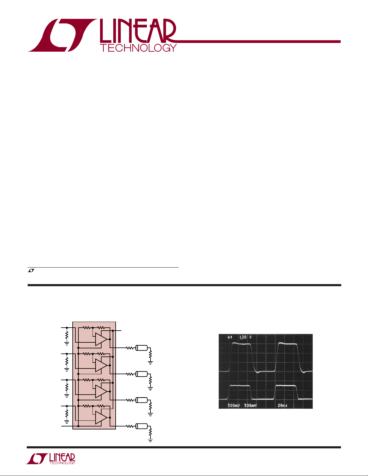
TYPICAL APPLICATIO
3.3V Single Supply LT6551 RGB Plus SYNC Cable Driver
LT6551
450Ω 450Ω
450Ω 450Ω
450Ω 450Ω
450Ω 450Ω
SYNC
GND
R
IN
75Ω
G
IN
75Ω
B
IN
75Ω
IN
75Ω
–
OA
+
–
OA
+
–
OA
+
–
OA
+
U
3.3V
75Ω
R
OUT
75Ω
75Ω
G
OUT
75Ω
75Ω
B
OUT
SYNC
OUT
75Ω
75Ω
75Ω
6551 TA01a
Output Step Response
65501fa
1
Page 2
LT6550/LT6551
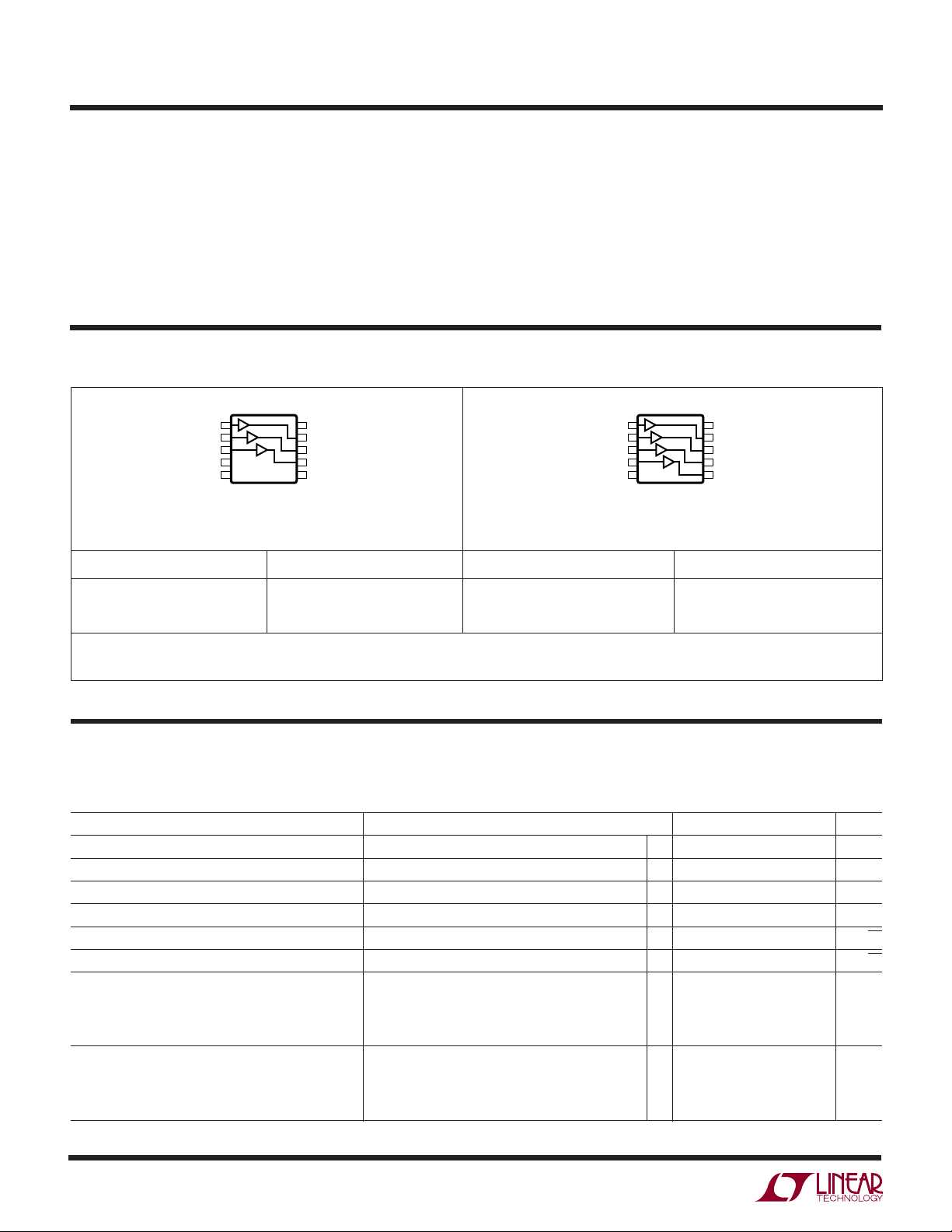
1
2
3
4
5
IN1
IN2
IN3
IN4
GND
10
9
8
7
6
V
CC
OUT1
OUT2
OUT3
OUT4
TOP VIEW
MS10 PACKAGE
10-LEAD PLASTIC MSOP
X2
X2
X2
X2
WW
W
U
ABSOLUTE AXI U RATI GS
(Note 1)
Total Supply Voltage
LT6550 (V
LT6551 (V
TO VEE)........................................ 12.6V
CC
TO GND) ...................................... 12.6V
CC
Input Current (Note 9) ........................................ ±10mA
Output Short-Circuit Duration (Note 2) ............ Indefinite
Operating Temperature Range ................ –40°C to 85°C
UUW
PACKAGE/ORDER I FOR ATIO
TOP VIEW
1
IN1
2
IN2
3
IN3
4
GND
5
V
EE
MS10 PACKAGE
10-LEAD PLASTIC MSOP
T
= 150°C, θJA = 110°C/W
JMAX
ORDER PART NUMBER
X2
X2
(Note 4)
10
V
CC
OUT1
9
X2
OUT2
8
OUT3
7
N/C
6
MS10 PART MARKING
Specified Temperature Range (Note 3)
LT6550C/LT6551C .............................. –40°C to 85°C
LT6550I/LT6551I................................ –40°C to 85°C
Maximum Junction Temperature .......................... 150°C
Storage Temperature Range ................. –65°C to 150°C
Lead Temperature (Soldering, 10 sec).................. 300°C
T
= 150°C, θJA = 110°C/W
JMAX
(Note 4)
ORDER PART NUMBER MS10 PART MARKING
Consult LTC Marketing for parts specified with wider operating temperature ranges.
3.3V ELECTRICAL CHARACTERISTICS
temperature range, otherwise specifications are at T
LT6551 (Pins 1,2,3,4). V
PARAMETER CONDITIONS MIN TYP MAX UNITS
DC Output Accuracy No Load, V
Output Voltage Matching Between Any Two Outputs
Input Current Any Input
Input Impedance, ∆VIN/∆I
Input Noise Voltage Density f = 100kHz (Note 10) 12 nV/√Hz
Input Noise Current Density f = 100kHz (Note 10) 8 pA/√Hz
Voltage Gain (Note 5) 0.25V ≤ VIN ≤ 1.25V
Output Voltage Swing Low VIN = –0.1V
2
LT6550CMS
LT6550IMS
Order Options Tape and Reel: Add #TR Lead Free: Add #PBF Lead Free Tape and Reel: Add #TRPBF
Lead Free Part Marking: http://www.linear.com/leadfree/
= 0V LT6550 (Pin 5), unless otherwise noted.
EE
IN
LTB9
LTC1
The
= 25°C. VCC = 3.3V, V
A
Ideal = 1.5V
OUT
VIN = 0V to 1V
No Load
= 150Ω
R
L
R
= 75Ω, 0.25V ≤ VIN ≤ 0.75V 1.85 2.15 V/V
L
No Load
= 5mA
I
SINK
I
= 10mA
SINK
LT6551CMS
LT6551IMS
●
denotes the specifications which apply over the specified
= 0V; VIN = 0.75V LT6550 (Pins 1,2,3);
GND
LTC2
LTC3
●
●
●
●
100 300 kΩ
●
1.9 2.1 V/V
●
1.9 2.1 V/V
●
●
●
30 70 mV
25 75 mV
15 65 µA
10 30 mV
60 150 mV
90 200 mV
65501fa
Page 3
LT6550/LT6551
3.3V ELECTRICAL CHARACTERISTICS
temperature range, otherwise specifications are at T
LT6551 (Pins 1,2,3,4). V
PARAMETER CONDITIONS MIN TYP MAX UNITS
Output Voltage Swing High VIN = 1.75V
PSRR VCC = 3V to 10V, VIN = 0.5V
Minimum Supply Voltage (Note 6)
Output Short-Circuit Current VIN = 1V, V
Supply Current per Amplifier (Note 7) 8.5 10 mA
Slew Rate (Note 8) RL = 150Ω, V
Small Signal –3dB Bandwidth RL = 150Ω 90 MHz
Gain Flatness Less than 0.25dB 30 MHz
Gain Matching Any One Channel to Any Other Channel 0.15 dB
Settling Time to 3% RL = 150Ω, V
Settling Time to 1% RL = 150Ω, V
% Overshoot V
Differential Gain RL = 150Ω, Black Level = 0.6V at Device Output 0.09 %
Differential Phase RL = 150Ω, Black Level = 0.6V at Device Output 0.09 Deg
Channel Separation Measured at 10MHz 60 dB
= 0V LT6550 (Pin 5), unless otherwise noted.
EE
Measured from 1V to 2V
= 25°C. VCC = 3.3V, V
A
No Load
R
= 150Ω
L
= 75Ω 2.0 2.5 V
R
L
= 0V 35 50 mA
OUT
= 0.5V to 2.5V 140 250 V/µs
OUT
= 1V to 2.5V 20 ns
OUT
= 1V to 2.5V 30 ns
OUT
= 1V to 2.5V, RL = 150Ω 5%
OUT
The ● denotes the specifications which apply over the specified
= 0V; VIN = 0.75V LT6550 (Pins 1,2,3);
GND
●
3.0 3.2 V
●
2.5 2.9 V
●
40 48 dB
●
3V
●
25 mA
●
●
115 V/µs
11 mA
5V ELECTRICAL CHARACTERISTICS
temperature range, otherwise specifications are at T
LT6551 (Pins 1,2,3,4). V
PARAMETER CONDITIONS MIN TYP MAX UNITS
Output Accuracy No Load, V
Output Voltage Matching Between Any Two Outputs
Input Current
Input Impedance, ∆VIN/∆I
Input Noise Voltage Density f = 100kHz (Note 10) 12 nV/√Hz
Input Noise Current Density f = 100kHz (Note 10) 8 pA/√Hz
Voltage Gain (Note 5) 0.25V ≤ VIN ≤ 1.75V
Output Voltage Swing Low VIN = –0.1V
Output Voltage Swing High VIN = 2.6V
= 0V LT6550 (Pin 5), unless otherwise noted.
EE
IN
VIN = 0V to 2V
No Load
R
R
No Load
I
SINK
I
SINK
No Load
R
R
= 25°C. VCC = 5V, V
A
OUT
= 150Ω
L
= 75Ω, 0.25V ≤ VIN ≤ 1.25V, 0°C ≤ TA ≤ 70°C (Only)
L
= 5mA
= 10mA
= 150Ω
L
= 75Ω, 0°C ≤ TA ≤ 70°C (Only)
L
The ● denotes the specifications which apply over the specified
= 0V; VIN = 1.25V LT6550 (Pins 1,2,3);
GND
Ideal = 2.5V
●
●
●
●
100 300 kΩ
●
1.9 2.1 V/V
●
1.9 2.1 V/V
●
1.85 2.15 V/V
●
●
●
●
4.6 4.8 V
●
3.5 4.1 V
●
2.5 3.2 V
30 70 mV
40 90 mV
15 65 µA
10 30 mV
60 150 mV
90 200 mV
65501fa
3
Page 4
LT6550/LT6551
5V ELECTRICAL CHARACTERISTICS
temperature range, otherwise specifications are at T
LT6551 (Pins 1,2,3,4). V
PARAMETER CONDITIONS MIN TYP MAX UNITS
PSRR VCC = 3V to 10V, VIN = 0.5V
Minimum Supply Voltage (Note 6)
Output Short-Circuit Current VIN = 1V, V
Supply Current per Amplifier (Note 7) 9.5 11.5 mA
Slew Rate RL = 150Ω, V
Small Signal –3dB Bandwidth RL = 150Ω 110 MHz
Gain Flatness Less than 0.25dB 30 MHz
Gain Matching Any One Channel to Any Other Channel 0.15 dB
Settling Time to 3% RL = 150Ω, V
Settling Time to 1% RL = 150Ω, V
% Overshoot V
Differential Gain RL = 150Ω, Black Level = 1V at Device Output 0.05 %
Differential Phase RL = 150Ω, Black Level = 1V at Device Output 0.05 Deg
Channel Separation Measured at 10MHz 60 dB
= 0V LT6550 (Pin 5), unless otherwise noted.
EE
= 25°C. VCC = 5V, V
A
≤ 70°C
0°C ≤ T
A
–40°C ≤ T
Measured from 1V to 3V
= 1V to 2.5V, RL = 150Ω 5%
OUT
The ● denotes the specifications which apply over the specified
= 0V; VIN = 1.25V LT6550 (Pins 1,2,3);
GND
●
40 48 dB
●
3V
= 0V 45 60 mA
OUT
≤ 85°C
A
= 0.5V to 3.5V, 220 340 V/µs
OUT
= 1V to 2.5V 20 ns
OUT
= 1V to 2.5V 35 ns
OUT
●
40 mA
●
30 mA
●
●
180 V/µs
12.5 mA
±5V ELECTRICAL CHARACTERISTICS
the specified temperature range, otherwise specifications are at T
(LT6550 Only) The ● denotes the specifications which apply over
= 25°C. VS = ±5V, VIN = 0V (Pins 1,2,3) V
A
= 0V (Pin 4) unless
GND
otherwise noted.
PARAMETER CONDITIONS MIN TYP MAX UNITS
Output Offset
Output Voltage Matching Between Any Two Outputs
Input Current
Input Impedance, ∆VIN/∆I
Input Noise Voltage Density f = 100kHz (Note 10) 12 nV/√Hz
Input Noise Current Density f = 100kHz (Note 10) 8 pA/√Hz
Voltage Gain –1.75V ≤ VIN ≤ 1.75V
Output Voltage Swing VIN = ±2.6V
PSRR VS = ±2.5V to ±5V,
Output Short-Circuit Current VO = 0V 45 60 mA
IN
VIN = –1V to 1V
No Load
= 150Ω
R
L
= 75Ω, –1V ≤ VIN ≤ 1V
R
L
No Load
= 150Ω
R
L
= 75Ω, 0°C ≤ TA ≤ 70°C (Only)
R
L
0°C ≤ T
≤ 70°C
A
–40°C ≤ T
≤ 85°C
A
●
●
●
●
200 500 kΩ
●
1.9 2.1 V/V
●
1.9 2.1 V/V
●
1.9 2.1 V/V
●
±4.6 ±4.8 V
●
±3.5 ±4.2 V
●
±2.6 ±3.2 V
●
38 48 dB
●
40 mA
●
30 mA
30 70 mV
20 60 mV
20 70 µA
4
65501fa
Page 5
LT6550/LT6551
±5V ELECTRICAL CHARACTERISTICS
the specified temperature range, otherwise specifications are at T
(LT6550 Only) The ● denotes the specifications which apply over
= 25°C. VS = ±5V, VIN = 0V (Pins 1,2,3) V
A
= 0V (Pin 4) unless
GND
otherwise noted.
PARAMETER CONDITIONS MIN TYP MAX UNITS
Supply Current per Amplifier 8.5 10.5 mA
●
Slew Rate RL = 150Ω, V
Measured from –2V to 2V
= –3V to 3V, 400 600 V/µs
OUT
●
300 V/µs
Small Signal –3dB Bandwidth RL = 150Ω 90 MHz
Gain Flatness Less than 0.25dB 30 MHz
Gain Matching Any One Channel to Any Other Channel 0.15 dB
Settling Time to 3% RL = 150Ω, V
Settling Time to 1% RL = 150Ω, V
% Overshoot V
= 1V to 2.5V, RL = 150Ω 5%
OUT
= 1V to 2.5V 20 ns
OUT
= 1V to 2.5V 30 ns
OUT
Differential Gain RL = 150Ω, Black Level = 0V at Device Output 0.15 %
Differential Phase RL = 150Ω, Black Level = 0V at Device Output 0.09 Deg
Channel Separation Measured at 10MHz 60 dB
Note 1: Absolute Maximum Ratings are those values beyond which the life
of a device may be impaired.
Note 2: A heat sink may be required to keep the junction temperature
below absolute maximum. This depends on the power supply voltage and
how many amplifiers are shorted.
Note 3: The LT6550C/LT6551C are guaranteed to meet specified
performance from 0°C to 70°C and are designed, characterized and
expected to meet specified performance from –40°C to 85°C but are not
tested or QA sampled at these temperatures. The LT6550I/LT6551I are
guaranteed to meet specified performance from –40°C to 85°C.
Note 4: Thermal resistance varies depending upon the amount of PC board
metal attached to Pin 5 of the device. θ
is specified for a 2500mm2 test
JA
board covered with 2oz copper on both sides.
Note 5: Gain is measured by changing the input voltage, and dividing the
change in output voltage by the change in input voltage.
Note 6: Minimum supply voltage is guaranteed by the PSRR test.
Note 7: The supply current specification includes additional output current
through the internal feedback and gain resistor.
Note 8: Guaranteed by correlation to slew rate at 5V and ±5V.
Note 9: The inputs are protected from ESD with diodes to the supplies.
Note 10: Noise is input referred, including internal gain resistors.
12 mA
UW
5V/3.3V TYPICAL PERFOR A CE CHARACTERISTICS
V
(Pin 5) = 0V (LT6550), GND (Pin 5) = 0V (LT6551)
EE
Supply Current Per Amplifier vs
Supply Voltage
14
VIN = 0.75V
= ∞
R
L
12
GND = 0V
10
8
6
4
SUPPLY CURRENT (mA)
2
0
0
34
2
1
TA = 25°C
V
(V)
CC
TA = 125°C
TA = –55°C
1098765
6550/51 G01
Output Voltage vs Input Voltage
(V)
OUT
V
3.5
3.0
2.5
2.0
1.5
1.0
0.5
VS = 3.3V, 0V
= 150Ω
R
L
0
0
0.2
0.4
0.6 0.8
TA = 125°C
VIN (V)
TA = 25°C
TA = –55°C
6550/51 G02
–10
–11
–12
–13
–14
–15
–16
INPUT BIAS (µA)
–17
–18
–19
2.01.81.61.41.21.0
–20
Input Bias Current vs
Temperature
VS = 5V, 0V
= 2.5V
V
OUT
25
–50
0
–25
TEMPERATURE (°C)
50
75
100
6550/51 G03
65501fa
125
5
Page 6

LT6550/LT6551
UW
5V/3.3V TYPICAL PERFOR A CE CHARACTERISTICS
V
(Pin 5) = 0V (LT6550), GND (Pin 5) = 0V (LT6551)
EE
Input Bias Current vs Input
Voltage
0
–5
–10
–15
INPUT BIAS CURRENT (µA)
–20
–25
0
0.2 0.4
INPUT VOLTAGE (V)
TA = 25°C
TA = –55°C
0.8
0.6 1.0 1.6
Output Saturation Voltage vs
Load Current (Output Low)
1
VS = 5V, 0V
= –0.1V
V
IN
TA = 125°C
0.1
OUTPUT SATURATION VOLTAGE (V)
0.01
0.01
TA = 25°C
0.10 10
SINKING LOAD CURRENT (mA)
1 100
TA = 125°C
1.2 1.4
TA = –55°C
6550/51 G04
6550/51 G07
Input Bias Current vs Input
Voltage
0
VS = 5V, 0VVS = 3.3V, 0V
–5
–10
–15
–20
INPUT BIAS CURRENT (µA)
–25
–30
0
0.5 1.0 1.5 2.0
INPUT VOLTAGE (V)
TA = 125°C
TA = 25°C
TA = –55°C
Output Short-Circuit Current
vs Temperature
90
VIN = 1V
85
80
75
70
65
60
55
50
OUTPUT SHORT-CIRCUIT CURRENT (mA)
45
–50 –25
VS = 5V, 0V
VS = 3.3V, 0V
0 25 50 125
TEMPERATURE (°C)
6550/51 G05
10075
6550/51 G08
2.5
Output Saturation Voltage vs
Load Current (Output High)
1
VS = 5V, 0V
= 2.6V
V
IN
TA = 125°C
0.1
OUTPUT SATURATION VOLTAGE (V)
0.01
0.01
TA = 25°C
TA = –55°C
0.1 10
SOURCING LOAD CURRENT (mA)
1100
Gain and Phase vs Frequency
10
VS = 3.3V, 0V
9
= 1.5V DC
V
OUT
= 150Ω
R
L
8
7
6
GAIN
5
GAIN (dB)
4
3
2
1
0
10k 100k
FREQUENCY (Hz)
PHASE
1M 100M 500M10M
6550/51 GO9
6550/51 G06
0
–20
–40
–60
–80
–100
–120
–140
–160
–180
–200
PHASE (DEG)
Gain Flatness vs Frequency
6.2
VS = 3.3V, 0V
= 1.5V DC
V
OUT
= 150Ω
R
L
6.1
6.0
GAIN (dB)
5.9
5.8
5.7
10k 1M 10M 100M
100k
FREQUENCY (Hz)
6
6550/51 G10
–3dB, –0.25dB Bandwidth vs
Temperature
140
V
= 1.5V DC
OUT
= 150Ω
R
L
120
100
80
60
BANDWIDTH (MHz)
40
20
0
–50 –25
0 25 50 125
TEMPERATURE (°C)
5V, 0V, –0.25dB
3.3V, 0V, –0.25dB
5V, 0V, –3dB
3.3V, 0V, –3dB
10075
6550/51 G11
–3dB Bandwidth vs V
180
V
= 1.5V DC
OUT
GND = 0V
= 150Ω
R
L
160
140
120
–3dB BANDWIDTH (MHz)
100
80
412
3
5
CC
678 10
VCC (V)
9
11
6550/51 G12
65501fa
Page 7

UW
5V/3.3V TYPICAL PERFOR A CE CHARACTERISTICS
V
(Pin 5) = 0V (LT6550), GND (Pin 5) = 0V (LT6551)
EE
LT6550/LT6551
Frequency Response with
Capacitive Loads
12
VS = 5V, 0V
11
= 2.5V DC
V
OUT
= 150Ω
R
L
10
9
8
7
GAIN (dB)
6
5
4
3
2
10k 100k
CL = 100pF
CL = 50pF
1M 100M 500M10M
FREQUENCY (Hz)
CL = 150pF
CL = 10pF
Power Supply Rejection Ratio vs
Frequency
60
50
+PSSR
40
30
20
10
POWER SUPPLY REJECTION RATIO (dB)
0
100k 100M
10k 1M 10M 1000M
FREQUENCY (Hz)
VS = 5V, 0V
= 2.5V DC
V
OUT
= 150Ω
R
L
6550/51 G13
6550/51 G16
Capacitive Load Handling,
Overshoot vs Capacitive Load
45
VS = 5V, 0V
40
35
30
25
20
OVERSHOOT (%)
15
10
5
0
10
RL = OPEN
RL = 150Ω
100 1000
CAPACITIVE LOAD (pF)
Output Impedance vs Frequency
100
VS = 5V, 0V
= 2.5V DC
V
OUT
10
1
OUTPUT IMPEDANCE (Ω)
0.1
10k 1M 10M 100M
100k
FREQUENCY (Hz)
6550/51 G14
6550/51 G17
Slew Rate vs Temperature
500
450
400
350
300
SLEW RATE (V/µs)
250
200
150
–50
5V, 0V, RISING
5V, 0V, FALLING
–25 0
3.3V, 0V, RISING
3.3V, 0V, FALLING
25 75
TEMPERATURE (°C)
RL = 150Ω
50 100 125
Channel Separation vs Frequency
100
90
80
70
60
50
GAIN(dB)
40
30
20
10
0
10k 1M 10M 1000M
100k 100M
FREQUENCY (Hz)
VS = 5V, 0V
= 150Ω
R
L
ANY CHANNEL PAIR
6550/51 G15
6550/51 G18
Gain Matching vs Frequency
0
–0.2
–0.4
–0.6
GAIN MATCHING(dB)
–0.8
VS = 3.3V, 0V
= 1.5V DC, ANY CHANNEL PAIR
V
OUT
–1.0
100k 100M
10k 1M 10M 1000M
FREQUENCY (Hz)
6550/51 G19
2nd and 3rd Harmonic Distortion
vs Frequency
–30
VS = 3.3V, 0V
= 2V
O
= 150Ω
L
(0.5V TO 2.5V)
P-P
FREQUENCY (Hz)
2ND
3RD
1M 10M
V
R
–40
–50
–60
–70
DISTORTION (dBc)
–80
–90
100k
6550/51 G20
Small Signal Response
= 20pF
C
L
= 5V, 0V
V
S
= 2.5V DC
V
OUT
= 150Ω
R
L
6550/51 G21
65501fa
7
Page 8

LT6550/LT6551
UW
5V/3.3V TYPICAL PERFOR A CE CHARACTERISTICS
(Pin 5) = 0V (LT6550), GND (Pin 5) = 0V (LT6551)
V
EE
Large Signal Response
CL = 20pF
= 5V, 0V
V
S
= 0.5V TO 3.5V
V
OUT
= 150Ω
R
L
6550/51 G22
UW
±5V TYPICAL PERFOR A CE CHARACTERISTICS
V
(Pin 4) = 0V
GND
Supply Current vs Total Supply
Voltage
14
V
= 0V
OUT
12
10
8
6
4
SUPPLY CURRENT (mA)
2
0
0
±2 ±3 ±4 ±5 ±6
±1
TOTAL SUPPLY VOLTAGE (V)
TA = 125°C
TA = 25°C
TA = –55°C
6550/51 G23
Input Bias Current vs Input
Voltage
–10
VS = ±5V
–15
–20
–25
INPUT BIAS CURRENT (µA)
–30
–1.5
–2.0 –1.0 0 1.0 2.0
–2.5
TA = 25°C
–0.5
INPUT VOLTAGE (V)
0.5
TA = 125°C
TA = –55°C
1.5
6550/51 G24
2.5
(LT6550 Only)
Output Offset Voltage vs
Temperature of Three Typical Units
60
VS = ±5V
= 0V
V
IN
50
40
30
20
10
0
OUTPUT OFFSET VOLTAGE (mV)
–10
–20
–25 25 75 125
–50
050
TEMPERATURE (°C)
100
6550/51 G25
Output Voltage Matching vs
Temperature of Three Typical Parts
25
VS = ±5V
= 0V
V
IN
ANY CHANNEL PAIR
20
15
10
5
OUTPUT VOLTAGE MATCHING (mV)
0
–50
–25 0
TEMPERATURE (°C)
50 100 125
25 75
8
6550/51 G26
Output Short-Circuit Current
vs Temperature Gain and Phase vs Frequency
95
VS = ±5V
= ±1V
V
IN
90
85
80
75
OUTPUT SHORT-CIRCUIT CURRENT (mA)
70
–50 25 75
SINKING
SOURCING
–25 0
50 100 125
TEMPERATURE (°C)
6550/51 G27
10
9
8
7
6
5
GAIN(dB)
4
3
2
VS = ±5V
V
OUT
1
= 150Ω
R
L
0
10k 1M 10M 1000M
GAIN
= 0V DC
100k 100M
FREQUENCY (Hz)
PHASE
6550/51 G28
0
–20
–40
–60
–80
–100
–120
–140
–160
–180
–200
65501fa
PHASE (DEG)
Page 9

UW
±5V TYPICAL PERFOR A CE CHARACTERISTICS
V
(Pin 4) = 0V
GND
Gain Flatness vs Frequency
6.2
VS = ±5V
= 0V DC
V
OUT
= 150Ω
R
L
6.1
6.0
GAIN (dB)
5.9
5.8
5.7
10k 1M 10M 100M
100k
FREQUENCY (Hz)
Slew Rate
800
VS = ±5V
= 150Ω
R
L
750
700
650
600
SLEW RATE (/V µs)
550
500
–50
–25 0
TEMPERATURE (°C)
RISING
FALLING
50 100 125
25 75
6550/51 G29
6550/51 G32
Gain Matching vs Frequency
0
–0.2
–0.4
–0.6
GAIN MATCHING(dB)
–0.8
VS = ±5V
ANY CHANNEL PAIR
–1.0
10k 1M 10M 1000M
100k 100M
FREQUENCY (Hz)
6550/51 G30
Power Supply Rejection Ratio vs
Frequency Output Impedance vs Frequency
60
50
40
30
20
10
0
POWER SUPPLY REJECTION RATIO (dB)
–10
+PSRR
10k 1M 10M 1000M
100k 100M
FREQUENCY (Hz)
VS = ±5V
V
OUT
= 150Ω
R
L
–PSRR
= 0V DC
6550/51 G33
LT6550/LT6551
(LT6550 Only)
Frequency Response with
Capacitive Loads
12
VS = ±5V
11
= 0V DC
V
OUT
= 150Ω
R
L
10
9
8
7
GAIN (dB)
6
5
4
3
2
10k 100k
MM
100
VS = ±5V
= 0V DC
V
OUT
10
1
OUTPUT IMPEDANCE (Ω)
0.1
10k 1M 10M 100M
100k
CL = 150pF
CL = 100pF
CL = 50pF
CL = 10pF
1M 100M 500M10M
FREQUENCY (Hz)
FREQUENCY (Hz)
6550/51 G31
6550/51 G34
Channel Separation vs Frequency
100
90
80
70
60
50
GAIN (dB)
40
30
20
10
0
10k 1M 10M 1000M
100k 100M
FREQUENCY (Hz)
VS = ±5V
= 150Ω
R
L
ANY CHANNEL PAIR
6550/51 G35
2nd and 3rd Harmonic Distortion
vs Frequency
–30
VS = ±5V
= 2V
O
= 150Ω
L
P-P
FREQUENCY (Hz)
2ND
3RD
1M 10M
V
R
–40
–50
–60
–70
DISTORTION (dBc)
–80
–90
100k
6550/51 G36
Large Signal Response
0V
CL = 20pF
= ±5V
V
S
= 150Ω
R
L
6550/51 G37
65501fa
9
Page 10

LT6550/LT6551
W
BLOCK DIAGRA S
IN1
IN2
IN3
GND
V
LT6550 Block Diagram
450Ω 450Ω
V
–
OA
+
450Ω 450Ω
–
OA
+
450Ω 450Ω
–
OA
+
EE
6550 BD01
CC
OUT1
OUT2
OUT3
N/C
IN1
IN2
IN3
IN4
GND
LT6551 Block Diagram
450Ω 450Ω
–
OA
+
450Ω 450Ω
–
OA
+
450Ω 450Ω
–
OA
+
450Ω 450Ω
–
OA
+
6551 BD02
V
CC
OUT1
OUT2
OUT3
OUT4
10
65501fa
Page 11

LT6550/LT6551
U
WUU
APPLICATIO S I FOR ATIO
Amplifier Characteristics
Figure 1 shows a simplified schematic of one channel of
the LT6551 quad. Resistors RF and RG provide an internal
gain of 2. (The LT6550 triple is a slight variation with the
gain setting resistor, RG, connected to a separate ground
pin). The input stage consists of transistors Q1 to Q8 and
resistor R1. This topology allows for high slew rates at low
supply voltages. There are back-to-back series diodes, D1
to D4, across the + and – inputs of each amplifier to limit
the differential input voltage to ±1.4V. R
current through these diodes if the input differential voltage exceeds ±1.4V. The input stage drives the degeneration resistors of PNP and NPN current mirrors, Q9 to Q12,
that convert the differential signals into a single-ended
output. The complementary drive generator supplies current to the output transistors that swing from rail-to-rail.
Input Voltage Range
The input voltage range is V
to (VCC – 1.75V) over
EE
temperature. If the device is operated on a single 3V supply
limits the
IN
the maximum input is (3V – 1.75V) or 1.25V, and the
internal gain of two will set the output voltage to 2.5V.
Increasing the input beyond 1.25V will force the device out
of its linear range, no longer a gain of 2, and the output will
not increase beyond 2.5V. At a higher supply voltage, i.e.
5V, the maximum input voltage is 5V – 1.75V or 3.25V.
However, due to the internal gain of 2, the output will clip
with a lower input voltage. For linear unclipped operation
the minimum input voltage is (V
mum input voltage is (V
OUT
Min)/2 and the maxi-
OUT
Max)/2 or (VCC – 1.75V),
whichever is less.
ESD
The LT6550/LT6551 have reverse-biased ESD protection
diodes on all inputs and outputs as shown in Figure 1. If
these pins are forced beyond either supply, unlimited
current will flow through these diodes. If the current is
limited to 10mA or less, no damage to the device will
occur.
DESD1
IN
DESD2
V
GND
+
V
GND
+
DESD3
DESD4
V
OUT
GND
6551 F01
RF
450Ω
+
R
IN
225Ω
D1
D2
RG
450Ω
I1 I2 I3
Q2
Q3Q4Q5
R1
+–
Q1
D3
D4
Q7
Q8
Q6
I4
Q9
Q11
R2 R3
Q10
Q12
R4 R5
Q13
CM
COMPLEMENTARY
DRIVE
GENERATOR
Q14
Figure 1. LT6551 Simplified Schematic
65501fa
11
Page 12

LT6550/LT6551
U
WUU
APPLICATIO S I FOR ATIO
Power Dissipation
The LT6550/LT6551, enhanced θ
Pin 5 (V
for the LT6550 and GND for the LT6551) fused
EE
to the lead frame. This thermal connection increases the
efficiency of the PC board as a heat sink. The PCB material
can be very effective at transmitting heat between the pad
area attached to Pin 5 and a ground or power plane layer.
Copper board stiffeners and plated through holes can also
be used to spread the heat generated by the device. Table 1
lists the thermal resistance for several different board
sizes and copper areas. All measurements were taken on
3/32” FR-4 board with 2oz copper. This data can be used
as a rough guideline in estimating thermal resistance. The
thermal resistance for each application will be affected by
thermal interactions with other components as well as
board size and shape.
Table 1. Fused 10-Lead MSOP Package
COPPER AREA
TOPSIDE* BACKSIDE BOARD AREA THERMAL RESISTANCE
(mm2) (mm2) (mm2) (JUNTION-TO-AMBIENT)
540 540 2500 110°C/W
100 100 2500 120°C/W
100 0 2500 130°C/W
30 0 2500 135°C/W
0 0 2500 140°C/W
*Device is mounted on topside.
As an example, calculate the junction temperature for the
circuit in Figure 2 assuming an 85°C ambient temperature.
The device dissipation can be found by measuring the
supply current, calculating the total dissipation and then
subtracting the dissipation in the load.
MS package, has
JA
The dissipation for the amplifiers is:
= (106mA)(5V) –4 • (2.5V)2/150 = 363mW
P
D
The total package power dissipation is 363mW. When a
2500 sq mm PC board with 540 sq mm of 2oz copper on
top and bottom is used, the thermal resistance is
110°C/W. The junction temperature (T
T
= (363mW)(110°C/W) + 85°C = 125°C
J
) is:
J
The maximum junction temperature for the LT6551 is
150°C so the heat sinking capability of the board is
adequate for the application.
LT6551
450Ω 450Ω
5V
–
OA
+
1.25V
GND
Figure 2. Calculating Junction Temperature
450Ω 450Ω
–
OA
+
450Ω 450Ω
–
OA
+
450Ω 450Ω
–
OA
+
75Ω
75Ω
75Ω
75Ω
75Ω
75Ω
75Ω
75Ω
6551 F02
12
65501fa
Page 13

TYPICAL APPLICATIO
LUMINANCE
U
470µF
75Ω
LT6550/LT6551
S Video Splitter
LT6551
4k
1k
1
2
450Ω 450Ω
–
OA
+
450Ω 450Ω
10
V
= 5V
CC
75Ω
9
LUMINANCE
OUT2
CHROMA
470µF
75Ω
= 5V
V
CC
4k
3
1k
450Ω 450Ω
4
5
–
OA
+
450Ω 450Ω
–
OA
+
–
OA
+
6551 TA02
8
7
6
75Ω
CHROMA
75Ω
75Ω
OUT1
CHROMA
OUT2
LUMINANCE
OUT1
S-VIDEO
CONNECTOR
OUT1
S-VIDEO
CONNECTOR
OUT2
65501fa
13
Page 14

LT6550/LT6551
TYPICAL APPLICATIO
U
Consumer products require generation of YPBPR luminance/chrominance component signals, often from RGB
source content. The YP
format has a luminance signal
BPR
and two weighted color difference signals at baseband.
Even with their fixed internal gain resistors, two LT6550s
connected as shown easily implement the required conversion matrix equations. The Y channel is a weighted
average of the 2X amplified RGB signals and with the
feedback connection of the Y channel output in the second
LT6550 back to the gain-resistor common pin, an implicit
Y subtraction is performed for the chroma channels and
RGB to YPBPR Component-Video Conversion
3.3V 3.3V
LT6550
10
450Ω 450Ω
the desired unity gain is produced for the Y-channel. The
necessary scaling of the color-difference signals is performed passively by their respective output termination
resistor networks. Since this circuit naturally produces
bipolar chroma signals (±0.35V at the cable load) regardless of RGB offset, the simplest implementation is to
power the circuit with ±3.3V split supplies. With an available output swing of about 5.6V for this supply configuration, the circuit handles video with composite syncs and/
or various offsets without difficulty.
LT6550
10
450Ω 450Ω
–3.3V
9
8
7
1070Ω
549Ω
2940Ω
1
2
3
45
= 0.713(R – Y)
P
R
≈ 44MHz
f
3dB
–
+
450Ω 450Ω
–
+
450Ω 450Ω
–
+
–3.3V
R
75Ω
G
75Ω
B
75Ω
1
2
3
45
–
+
450Ω 450Ω
–
+
450Ω 450Ω
–
+
Y = 0.299R + 0.587G + 0.114B
= 0.565(B – Y)
P
B
105Ω
9
261Ω
75Ω
8
133Ω
7
174Ω
6550/51 TAO3
P
R
Y
P
B
14
65501fa
Page 15

PACKAGE DESCRIPTIO
U
MS Package
10-Lead Plastic MSOP
(Reference LTC DWG # 05-08-1661)
0.889 ± 0.127
(.035 ± .005)
LT6550/LT6551
5.23
(.206)
MIN
0.305 ± 0.038
(.0120 ± .0015)
TYP
RECOMMENDED SOLDER PAD LAYOUT
0.254
(.010)
GAUGE PLANE
0.18
(.007)
NOTE:
1. DIMENSIONS IN MILLIMETER/(INCH)
2. DRAWING NOT TO SCALE
3. DIMENSION DOES NOT INCLUDE MOLD FLASH, PROTRUSIONS OR GATE BURRS.
MOLD FLASH, PROTRUSIONS OR GATE BURRS SHALL NOT EXCEED 0.152mm (.006") PER SIDE
4. DIMENSION DOES NOT INCLUDE INTERLEAD FLASH OR PROTRUSIONS.
INTERLEAD FLASH OR PROTRUSIONS SHALL NOT EXCEED 0.152mm (.006") PER SIDE
5. LEAD COPLANARITY (BOTTOM OF LEADS AFTER FORMING) SHALL BE 0.102mm (.004") MAX
3.20 – 3.45
(.126 – .136)
DETAIL “A”
DETAIL “A”
0.50
(.0197)
BSC
0° – 6° TYP
0.53 ± 0.152
(.021 ± .006)
SEATING
PLANE
3.00 ± 0.102
(.118 ± .004)
(NOTE 3)
4.90 ± 0.152
(.193 ± .006)
(.043)
0.17 – 0.27
(.007 – .011)
TYP
1.10
MAX
12
0.50
(.0197)
BSC
0.497 ± 0.076
7
6
45
(.0196 ± .003)
REF
3.00 ± 0.102
(.118 ± .004)
(NOTE 4)
0.86
(.034)
REF
0.127
± 0.076
(.005 ± .003)
MSOP (MS) 0603
8910
3
Information furnished by Linear Technology Corporation is believed to be accurate and reliable.
However, no responsibility is assumed for its use. Linear Technology Corporation makes no representation that the interconnection of its circuits as described herein will not infringe on existing patent rights.
65501fa
15
Page 16

LT6550/LT6551
TYPICAL APPLICATIO
10MHz LABORATORY
FREQUENCY REFERENCE
U
(4dBm MAX)
10MHz Reference Distribution Amplifier
LT6551
1
450Ω 450Ω
–
OA
+
450Ω 450Ω
50Ω
4.53k
10nF
1k
10
9
50Ω
10nF
V
CC
= 3.3V
2
3
4
5
–
OA
+
450Ω 450Ω
–
OA
+
450Ω 450Ω
–
OA
+
8
50Ω
10nF
7
50Ω
10nF
7
50Ω
10nF
6550/51 TA04
RELATED PARTS
PART NUMBER DESCRIPTION COMMENTS
LT1259/LT1260 Dual/Triple 130MHz Current Feedback Amplifiers Shutdown, Operates to ±15V
LT1395/LT1396/LT1397 Single, Dual, Quad 400MHz Current Feedback Amplifier 800V/µs Slew Rate
LT1398/LT1399 Dual/Triple 300MHz Current Feedback Amplifier 0.1dB Gain Flatness to 150MHz, Shutdown
LT1675/LT1675-1 250MHz, Triple and Single RGB Multiplexer with 100MHz Pixel Switching, –3dB Bandwidth: 250MHz,
Current Feedback Amplifiers 1100V/µs Slew Rate
LT1809/LT1810 Single/Dual, 180MHz, Rail-to-Rail Input and 350V/µs Slew Rate, Shutdown,
Output Amplifiers Low Distortion –90dBc at 5MHz
16
Linear Technology Corporation
1630 McCarthy Blvd., Milpitas, CA 95035-7417
(408) 432-1900 ● FAX: (408) 434-0507
●
www.linear.com
65501fa
LT 1105 REV A • PRINTED IN USA
© LINEAR TECHNOLOGY CORPORATION 2005
 Loading...