

LT6411
650MHz Differential ADC
Driver/Dual Selectable
Gain Amplifi er
FEATURES
■
650MHz –3dB Small-Signal Bandwidth
■
600MHz –3dB Large-Signal Bandwidth
■
High Slew Rate: 3300V/µs
■
Easily Confi gured for Single-Ended to Differential
Conversion
■
200MHz ±0.1dB Bandwidth
■
User Selectable Gain of +1, +2 and –1
■
No External Resistors Required
■
46.5dBm Equivalent OIP3 at 30MHz When Driving an
ADC
■
IM3 with 2V
–87dBc at 30MHz, –83dBc at 70MHz
■
–77dB SFDR at 30MHz, 2V
■
6ns 0.1% Settling Time for 2V Step
■
Low Supply Current: 8mA per Ampifi er
■
Differential Gain of 0.02%, Differential Phase of 0.01°
■
50dB Channel Separation at 100MHz
■
Wide Supply Range: ±2.25V (4.5V) to ±6.3V (12.6V)
■
3mm × 3mm 16-Pin QFN Package
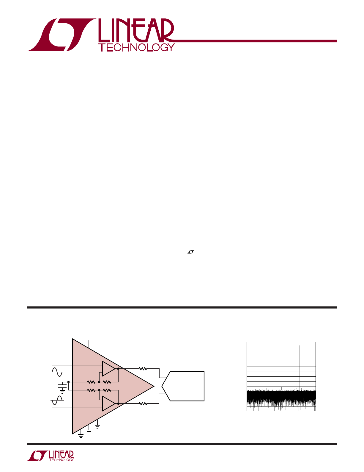
Composite, Differential Output:
P-P
Differential Output
P-P
DESCRIPTION
The LT®6411 is a dual amplifi er with individually selectable
gains of +1, +2 and –1. The amplifi ers have excellent distortion performance for driving ADCs as well as excellent
bandwidth and slew rate for video, data transmission and
other high speed applications. Single-ended to differential
conversion with a system gain of 2 is particularly straightforward by confi guring one amplifi er with a gain of +1
and the other amplifi er with a gain of –1. The LT6411 can
be used on split supplies as large as ±6V and on a single
supply as low as 4.5V.
Each amplifi er draws only 8mA of quiescent current when
enabled. When disabled, the output pins become high
impedance and each amplifi er draws less than 350µA.
The LT6411 is manufactured on Linear Technology’s
proprietary, low voltage, complimentary, bipolar process
and is available in the ultra-compact, 3mm × 3mm, 16pin
QFN package.
, LT, LTC and LTM are registered trademarks of Linear Technology Corporation.
All other trademarks are the property of their respective owners.
APPLICATIONS
■
Differential ADC Driver
■
Single-Ended to Differential Conversion
■
Differential Video Line Driver
TYPICAL APPLICATION
Differential ADC Driver
5V
V
CC
1.9V
1.9V
DC
30MHz
INPUT
DC
LT6411
DGND
EN
+
–
370Ω 370Ω
370Ω 370Ω
–
+
V
EE
24Ω
24Ω
A
IN
A
IN
–
LTC2249
14-BIT ADC
80Msps
+
6411 TA01a
30MHz 2-Tone 32768 Point FFT, LT6411
Driving an LTC®2249 14-Bit ADC
0
32768 POINT FFT
–10
TONE 1 AT 29.5MHz, –7dBFS
–20
TONE 2 AT 30.5MHz, –7dBFS
–30
IM3 = –87dBc
–40
–50
–60
–70
–80
–90
AMPLITUDE (dBFS)
–100
–110
–120
–130
–140
10
5
0
FREQUENCY (MHz)
25
20 40
15
30 35
6411 TA01b
6411f
1
LT6411
(Note 1)
Total Supply Voltage (VCC to VEE) ..........................12.6V
Input Current (Note 2) ..........................................±10mA
Output Current (Continuous) ...............................±70mA
EN to DGND Voltage (Note 2) ..................................5.5V
Output Short-Circuit Duration (Note 3) ............ Indefi nite
Operating Temperature Range (Note 4) ... –40°C to 85°C
Specifi ed Temperature Range (Note 5) ....–40°C to 85°C
Storage Temperature Range ................... –65°C to 125°C
Junction Temperature ........................................... 125°C
PACKAGE/ORDER INFORMATIONABSOLUTE MAXIMUM RATINGS
TOP VIEW
IN2+IN2–IN1–IN1
16
1
V
EE
2
V
EE
3
V
EE
4
NC
5678
OUT2
16-LEAD (3mm × 3mm) PLASTIC QFN
T
JMAX
EXPOSED PAD (PIN 17) IS V
UD PACKAGE
= 125°C, θJA = 68°C/W, θJC = 4.2°C/W
ORDER PART NUMBER UD PART MARKING*
+
15 14
13
12
DGND
11
17
CC
V
V
, MUST BE SOLDERED TO PCB
EE
EN
10
V
CC
9
VCC
EE
OUT1
LT6411CUD
LT6411IUD
LCGP
LCGP
Order Options Tape and Reel: Add #TR
Lead Free: Add #PBF Lead Free Tape and Reel: Add #TRPBF
Lead Free Part Marking: http://www.linear.com/leadfree/
Consult LTC Marketing for parts specifi ed with wider operating temperature ranges.
*Temperature grade is identifi ed by a label on the shipping container.
ELECTRICAL CHARACTERISTICS
The
temperature range, otherwise specifi cations are at T
= 25°C. VS = ±5V, AV = 2, RL = 150Ω, CL = 1.5pF, VEN = 0.4V, V
A
●
denotes the specifi cations which apply over the full operating
= 0V,
DGND
unless otherwise noted.
SYMBOL PARAMETER CONDITIONS MIN TYP MAX UNITS
V
I
R
C
V
OS
IN
IN
IN
CMR
Input Referred Offset Voltage VIN = 0V, VOS = V
Input Current
Input Resistance VIN = ±1V
Input Capacitance f = 100kHz 1 pF
Maximum Input Common Mode Voltage
Minimum Input Common Mode Voltage
PSRR Power Supply Rejection Ratio V
I
PSRR
ERR Gain Error V
A
V
A
MATCH Gain Matching V
V
V
OUT
I
S
Input Current Power Supply Rejection VS (Total) = 4.5V to 12V (Note 6)
Maximum Output Voltage Swing RL = 1k
Supply Current, Per Amplifi er
Supply Current, Disabled, per Amplifi er V
I
EN
Enable Pin Current VEN = 0.4V
(Total) = 4.5V to 12V (Note 6)
S
= ±2V
OUT
= ±2V ±1 %
OUT
R
= 150Ω
L
R
= 150Ω
L
= 4V
EN
V
= Open
EN
+
= V
V
EN
OUT
/2
●
●
●
150 500 kΩ
●
56 62 dB
●
●
±3.70
±3.25
●
±3.10
3 ±10
±20
–17 ±50 µA
V
– 1
CC
+ 1
V
EE
1 ±4 µA/V
–1.2 ±5 %
±3.95
±3.6
mV
mV
81114mA
●
●
●
●
–200 –95
●
22
0.5
350
350
0.5 50
mA
µA
µA
µA
µA
6411f
V
V
V
V
V
2
LT6411
ELECTRICAL CHARACTERISTICS
The
temperature range, otherwise specifi cations are at T
= 25°C. VS = ±5V, AV = 2, RL = 150Ω, CL = 1.5pF, VEN = 0.4V, V
A
unless otherwise noted.
SYMBOL PARAMETER CONDITIONS MIN TYP MAX UNITS
I
SC
SR Slew Rate ±1V on ±2V Output Step (Note 9) 1700 3300 V/µs
–3dB BW Small-Signal –3dB Bandwidth V
0.1dB BW Gain Flatness ±0.1dB Bandwidth V
FPBW Full Power Bandwidth 2V Differential V
t
s
, t
t
r
f
dG Differential Gain (Note 8) 0.02 %
dP Diffi erential Phase (Note 8) 0.01 Deg
Output Short-Circuit Current RL = 0Ω, VIN = ±1V
= 200mV
OUT
= 200mV
OUT
= 2V
OUT
Full Power Bandwidth 2V V
Full Power Bandwidth 4V V
OUT
OUT
= 2V
= 4V
All Hostile Crosstalk f = 10MHz, V
f = 100MHz, V
Settling Time 0.1% to V
Small-Signal Rise and Fall Time 10% to 90%, V
●
denotes the specifi cations which apply over the full operating
= 0V,
DGND
●
±50 ±105 mA
, Single Ended 650 MHz
P-P
, Single Ended 200 MHz
P-P
Differential, –3dB 600 MHz
P-P
(Note 7) 270 525 MHz
P-P
(Note 7) 263 MHz
P-P
OUT
FINAL
= 2V
P-P
= 2V
OUT
P-P
, V
= 2V 6 ns
STEP
= 200mV
OUT
P-P
–75
–50
550 ps
dB
dB
The ● denotes the specifi cations which apply over the full operating temperature range, otherwise specifi cations are at TA = 25°C.
= 5V, VEE = 0V, AV = 2, No R
V
CC
SYMBOL PARAMETER CONDITIONS MIN TYP MAX UNITS
Noise/Harmonic Performance Input/Output Characteristics
1MHz Signal
HD Second/Third Harmonic Distortion 2V
IMD3
OIP3
Third-Order IMD 2V
1M
Output Third-Order Intercept Differential, f1 = 0.95MHz, f2 = 1.05MHz (Note 10) 49.5 dBm
1M
NF Noise Figure Single Ended 25.1 dB
e
n1M
Input Referred Noise Voltage Density 8 nV/√Hz
P1dB 1dB Compression Point (Note 10) 19.5 dBm
10MHz Signal
HD Second/Third Harmonic Distortion 2V
IMD3
OIP3
Third-Order IMD 2V
10M
Output Third-Order Intercept Differential, f1 = 9.5MHz, f2 = 10.5MHz (Note 10) 49 dBm
10M
NF Noise Figure Single Ended 24.7 dB
e
n10M
Input Referred Noise Voltage Density 7.7 nV/√Hz
P1dB 1dB Compression Point (Note 10) 19.5 dBm
, VEN = 0.4V, V
LOAD
= 0V, unless otherwise noted.
DGND
Differential
P-P
2V
Differential, RL = 200Ω Differential
P-P
Differential Composite, f1 = 0.95MHz,
P-P
f2 = 1.05MHz
2V
Differential Composite, f1 = 0.95MHz,
P-P
f2 = 1.05MHz, R
Differential
P-P
2V
Differential, RL = 200Ω Differential
P-P
Differential Composite, RL = 1k,
P-P
= 200Ω Differential
L
f1 = 9.5MHz, f2 = 10.5MHz
2V
Differential Composite, f1 = 9.5MHz,
P-P
f2 = 10.5MHz, R
= 200Ω Differential
L
–88
–87
dBc
dBc
–93 dBc
–91 dBc
–85
–76
dBc
dBc
–92 dBc
–89 dBc
6411f
3
LT6411
ELECTRICAL CHARACTERISTICS
The
temperature range, otherwise specifi cations are at T
= 25°C. VCC = 5V, VEE = 0V, AV = 2, No R
A
unless otherwise noted.
SYMBOL PARAMETER CONDITIONS MIN TYP MAX UNITS
30MHz Signal
HD Second/Third Harmonic Distortion 2V
IMD3
OIP3
NF Noise Figure Single Ended 24.6 dB
e
n30M
P1dB 1dB Compression Point (Note 10) 19.5 dBm
70MHz Signal
HD Second/Third Harmonic Distortion 2V
IMD3
OIP3
NF Noise Figure Single Ended 24.7 dB
e
n70M
P1dB 1dB Compression Point (Note 10) 19.5 dBm
Third-Order IMD 2V
30M
Output Third-Order Intercept Differential, f1 = 29.5MHz, f2 = 30.5MHz (Note 10) 46.5 dBm
30M
Input Referred Noise Voltage Density 7.6 nV/√Hz
Third-Order IMD 2V
70M
Output Third-Order Intercept Differential, f1 = 69.5MHz, f2 = 70.5MHz (Note 10) 44.5 dBm
70M
Input Referred Noise Voltage Density 7.7 nV/√Hz
Differential
P-P
2V
Differential, RL = 200Ω Differential
P-P
Differential Composite, f1 = 29.5MHz,
P-P
Differential, f2 = 30.5MHz
Differential Composite, f1 = 29.5MHz,
2V
P-P
f2 = 30.5MHz, R
Differential
P-P
2V
Differential, RL = 200Ω Differential
P-P
Differential Composite, f1 = 69.5MHz,
P-P
Differential, f2 = 70.5MHz
2V
Differential Composite, f1 = 69.5MHz,
P-P
f2 = 70.5MHz, R
●
denotes the specifi cations which apply over the full operating
= 200Ω Differential
L
= 200Ω Differential
L
, VEN = 0.4V, V
LOAD
= 0V,
DGND
–77
–64
–87 dBc
–75 dBc
–63
–52
–83 dBc
–64 dBc
dBc
dBc
dBc
dBc
Note 1: Stresses beyond those listed under Absolute Maximum Ratings
may cause permanent damage to the device. Exposure to any Absolute
Maximum Rating condition for extended periods may affect device
reliability and lifetime.
Note 2: This parameter is guaranteed to meet specifi ed performance
through design and characterization. It is not production tested.
Note 3: As long as output current and junction temperature are kept
below the Absolute Maximum Ratings, no damage to the part will occur.
Depending on the supply voltage, a heat sink may be required.
Note 4: The LT6411C is guaranteed functional over the operating
temperature range of –40°C to 85°C.
Note 5: The LT6411C is guaranteed to meet specifi ed performance from
0°C to 70°C. The LT6411C is designed, characterized and expected to
meet specifi ed performance from –40°C and 85°C but is not tested or
QA sampled at these temperatures. The LT6411I is guaranteed to meet
specifi ed performance from –40°C to 85°C.
Note 6: The two supply voltage settings for power supply rejection
are shifted from the typical ±V
measurement is taken at V
headroom for the enable circuitry to function with EN, DGND and all inputs
connected to 0V. The second measurement is taken at V
points for ease of testing. The fi rst
S
= 3V, VEE = –1.5V to provide the required 3V
CC
= 8V, VEE = –4V.
CC
Note 7: Full power bandwidth is calculated from the slew rate:
FPBW = SR/(π • V
Note 8: Differential gain and phase are measured using a Tektronix
TSG120YC/NTSC signal generator and a Tektronix 1780R video
measurement set. The resolution of this equipment is better than 0.05%
and 0.05°. Ten identical amplifi er stages were cascaded giving an effective
resolution of better than 0.005% and 0.005°.
Note 9: Slew rate is 100% production tested on channel 1. Slew rate of
channel 2 is guaranteed through design and characterization.
Note 10: Since the LT6411 is a feedback amplifi er with low output
impedance, a resistive load is not required when driving an ADC.
Therefore, typical output power is very small. In order to compare the
LT6411 with typical g
LT6411 output voltage swing driving an ADC is converted to OIP3 and
P1dB as if it were driving a 50Ω load.
)
P-P
amplifi ers that require 50Ω output loading, the
m
6411f
4
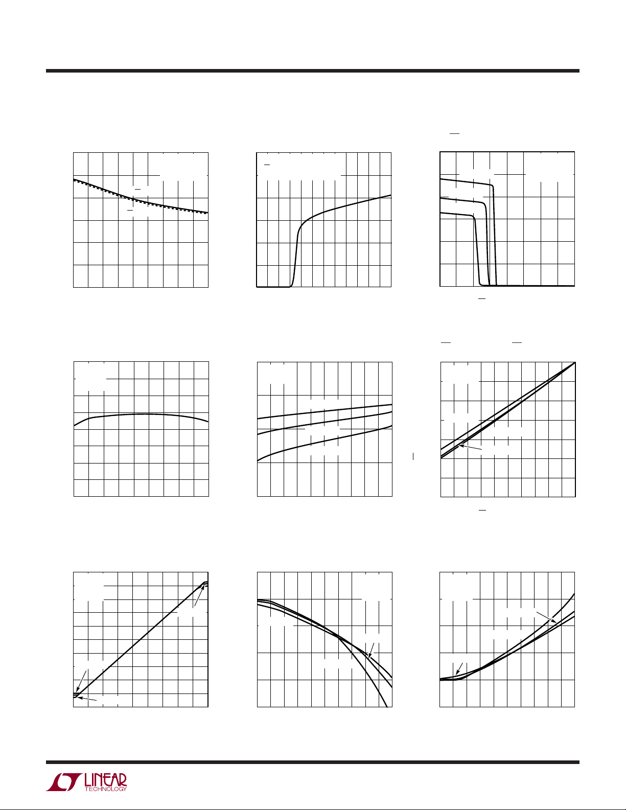
TYPICAL PERFORMANCE CHARACTERISTICS
All measurements are per amplifi er with single-ended outputs unless otherwise noted.
LT6411
Supply Current per Amplifi er
vs Temperature
12
10
V
8
6
4
SUPPLY CURRENT (mA)
2
0
–35 5
–55 –15
EN
= 0.4V
V
EN
25
TEMPERATURE (°C)
Output Offset Voltage
vs Temperature
20
VS = ±5V
= 0V
V
IN
15
= 2
A
V
10
5
0
–5
OFFSET VOLTAGE (mV)
–10
–15
–20
–35 5
–55 –15
25
TEMPERATURE (°C)
VS = ±5V
= ∞
R
L
+
–
, V
= 0V
V
IN
IN
= 0V
85
45
45 125
105
65
6411 G01
85
105
65
6411 G04
125
Supply Current per Ampifi er
vs Supply Voltage
12
= –V
V
CC
EE
VEN, V
= 25°C
T
10
A
8
6
4
SUPPLY CURRENT (mA)
2
0
0123456
+
, V
DGND
, V
IN
TOTAL SUPPLY VOLTAGE (V)
Positive Input Bias Current
vs Input Voltage
20
VS = ±5V
= 2
A
V
0
–20
BIAS CURRENT (µA)
+
IN
–40
–60
–2.5
–1.5
TA = 125°C
TA = 25°C
TA = –55°C
–0.5
INPUT VOLTAGE (V)
–
= 0V
IN
7 8 9 10 11 12
0.5
1.5
6411 G02
6411 G05
2.5
Supply Current per Amplifi er
vs EN Pin Voltage
12
10
SUPPLY CURRENT (mA)
TA = –55°C
TA = 25°C
8
TA = 125°C
6
4
2
0
0 0.5 1.0 1.5 2.0
EN PIN VOLTAGE (V)
2.5 3.0 3.5 4.0
EN Pin Current vs EN Pin Voltage
0
VS = ±5V
= 0V
V
DGND
–20
–40
TA = 125°C
–60
TA = –55°C
TA = 25°C
2
1
EN PIN VOLTAGE (V)
34
EN PIN CURRENT (µA)
–100
–120
–140
–80
0
VS = ±5V
V
DGND
+
, V
V
IN
= 0V
IN
–
= 0V
6411 G03
5
6411 G06
Output Voltage vs Input Voltage
5
VS = ±5V
4
= 1k
R
L
A
= 1
V
3
2
1
0
–1
TA = –55°C
–2
OUTPUT VOLTAGE (V)
–3
–4
–5
–3.5 –1.5
–4.5
TA = 125°C
–2.5
–0.5
INPUT VOLTAGE (V)
0.5 4.5
1.5
TA = 25°C
2.5
3.5
6411 G07
Output Voltage Swing vs I
(Output High)
5
4
TA = –55°C
3
2
OUTPUT VOLTAGE (V)
1
0
10
30
0
40
20
SOURCE CURRENT (mA)
TA = 125°C
LOAD
VS = ±5V
= 2
A
V
= 2V
V
IN
TA = 25°C
6411 G08
Output Voltage Swing vs I
LOAD
(Output Low)
0
VS = ±5V
= 2
A
V
= –2V
V
IN
–1
TA = 25°C
–2
–3
TA = –55°C
OUTPUT VOLTAGE (V)
–4
–5
102030
10050 60 70 80 90
040
TA = 125°C
10050 60 70 80 90
SINK CURRENT (mA)
6411 G09
6411f
5

LT6411
TYPICAL PERFORMANCE CHARACTERISTICS
All measurements are per amplifi er with single-ended outputs unless otherwise noted.
Positive Input Impedance
Input Noise Spectral Density
1000
100
e
i
10
INPUT NOISE (nV/√Hz OR pA/√Hz)
n
VS = ±5V
= 2
A
V
= 25°C
T
A
n
vs Frequency
1000
100
10
INPUT IMPEDANCE (kΩ)
1
VS = ±5V
= 0V
V
IN
= 25°C
T
A
PSRR vs Frequency
70
60
50
–PSRR
40
30
20
REJECTION RATIO (dB)
10
±PSRR
+PSRR
VS = ±5V
= 2
A
V
= 25°C
T
A
1
0.001 0.01 1 10 1000.1
FREQUENCY (kHz)
Frequency Response
vs Gain Confi guration
9
AV = 2, V
6
3
GAIN (dB)
0
–3
–6
0.1 10 100 1000
AV = 2, V
AV = 1, AV = –1,V
VS = ±5V
= 150Ω
R
L
= 25°C
T
A
1
OUT
OUT
AV = 1, V
AV = –1, V
FREQUENCY (MHz)
= 200mV
= 200mV
OUT
= 2V
OUT
OUT
P-P
P-P
= 2V
P-P
Harmonic Distortion vs Frequency,
Differential Input
0
V
= 2V
OUT
–10
= 2, VCC = 5V
A
V
V
EE
–20
DIFFERENTIAL R
TA = 25°C
–30
–40
–50
–60
DISTORTION (dBc)
–70
HD2, RL = 200Ω
–80
–90
–100
1
, DIFFERENTIAL
P-P
= 0V, VCM = 1.6V
LOAD
HD3, RL = ∞
FREQUENCY (MHz)
HD3, RL = 200Ω
HD2, RL = ∞
10 100
= 2V
P-P
6553 G10
P-P
6411 G13
6411 G16
0.1
0.01 0.1
FREQUENCY (MHz)
10 100 10001
Gain Flatness vs Frequency
6.5
VS = ±5V
6.4
= 2
A
V
= 200mV
V
OUT
6.3
RL = 150Ω
= 25°C
T
6.2
A
6.1
6.0
5.9
5.8
NORMALIZED GAIN (dB)
5.7
5.6
5.5
0.1 10 100 1000
P-P
CHANNEL 1
CHANNEL 2
1
FREQUENCY (MHz)
Harmonic Distortion vs Amplitude,
30MHz, Differential Input
0
AV = 2, VCC = 5V
–10
= 0V, VCM = 1.6V
V
EE
= ∞
R
L
–20
= 25°C
T
A
–30
–40
–50
–60
DISTORTION (dBc)
–70
–80
–90
–100
0.4
0.6 1.0
0.8
DIFFERENTIAL OUTPUT AMPLITUDE (V
1.2
1.4
HD3
HD2
1.6
1.8
6411 G11
6411 G14
P-P
6411 G17
2.0
)
0
0.001 0.01 1 10 1000.1
FREQUENCY (MHz)
Frequency Response with
Capacitive Loads
18
V
= ±5V
S
16
= 2
A
V
= 2V
V
14
OUT
P-P
RL = 150Ω
12
= 25°C
T
A
10
8
6
4
AMPLITUDE (dB)
2
0
–2
–4
–6
0.1 1 10 100 1000
CL = 6.8pF
CL = 2.2pF
FREQUENCY (MHz)
Harmonic Distortion vs Load,
30MHz, Differential Input
0
V
= 2V
OUT
–10
= 2, VCC = 5V
A
V
V
EE
–20
= 25°C
T
A
–30
–40
–50
–60
DISTORTION (dBc)
–70
–80
–90
–100
0
, DIFFERENTIAL
P-P
= 0V, VCM = 1.6V
200100
400300
DIFFERENTIAL R
500
600
700 900
(Ω)
LOAD
HD3
CL = 12pF
6553 G15
HD2
800
1011 G06
6411 G12
1000
6
6411f

0
TYPICAL PERFORMANCE CHARACTERISTICS
All measurements are per amplifi er with single-ended outputs unless otherwise noted.
Third Order Intermodulation
Distortion vs Frequency,
Differential Input
0
V
= 2V
OUT
–10
1MHz TONE SPACING
= 2, VCC = 5V
A
V
–20
V
EE
–30
DIFFERENTIAL R
TA = 25°C
–40
–50
–60
–70
THIRD ORDER IMD (dBc)
–80
–90
–100
0
, COMPOSITE, DIFFERENTIAL
P-P
= 0V, VCM = 1.6V
10
LOAD
RL = 200Ω
30
20
FREQUENCY (MHz)
40
Small-Signal Transient Response
0.15
0.10
0.05
0
OUTPUT (V)
–0.05
–0.10
–0.15
4 8 12 16
TIME (ns)
RL = ∞
50
60
VIN = 100mV
AV = 2
= ±5V
V
S
= 150Ω
R
L
= 25°C
T
A
70
6411 G19
P-P
2020 6 10 14 18
6411 G22
Output Third Order Intercept
vs Frequency, Differential Input
60
RL = ∞
RL = 200Ω
, COMPOSITE, DIFFERENTIAL
LOAD
40 60 70
30 50
FREQUENCY (MHz)
6411 G20
50
40
30
OIP3 (dBm)
V
OUT
20
1MHz TONE SPACING
A
V
V
EE
10
DIFFERENTIAL R
TA = 25°C
0
0
COMPUTED FOR 50Ω ENVIRONMENT
= 2V
P-P
= 2, VCC = 5V
= 0V, VCM = 1.6V
10 20
Video Amplitude Transient
Response Large-Signal Transient Response
2.0
1.5
1.0
0.5
OUTPUT (V)
0
–0.5
0
246
810
TIME (ns)
VIN = 700mV
AV = 2
= ±5V
V
S
= 150Ω
R
L
= 25°C
T
A
12 14 18
16
P-P
6411 G23
LT6411
Output Impedance vs Frequency
1000
100
10
1
OUTPUT IMPEDANCE (Ω)
0.1
0.01
4
3
2
1
0
OUTPUT (V)
–1
–2
–3
20
– 4
0
DISABLED
= 4V
V
EN
ENABLED
= 0.4V
V
EN
0.1
1
FREQUENCY (MHz)
4 8 12 20142 6 10 18
TIME (ns)
10
VS = ±5V
= 150Ω
R
L
= 25°C
T
A
100
VIN = 2.5V
AV = 2
= ±5V
V
S
= 150Ω
R
L
= 25°C
T
A
16
100
6411 G21
P-P
6411 G24
Crosstalk vs Frequency
0
VS = ±5V
= 2V
V
OUT
RL = 150Ω
= 25°C
T
A
DRIVE 2
LISTEN 1
P-P
10 100
FREQUENCY (MHz)
–20
–40
–60
AMPLITUDE (dB)
–80
–100
–120
1
DRIVE 1
LISTEN 2
Gain Error Distribution
40
VS = ±5V
= ±2V
V
OUT
35
= 150Ω
R
L
= 25°C
T
A
30
25
20
15
PERCENT OF UNITS (%)
10
5
0
1000
1635 G25
–3.0
–2.0 –1.0
GAIN ERROR–INDIVIDUAL CHANNEL (%)
0
1.0 2.0
3.0
6411 G26
Gain Matching Distribution
35
VS = ±5V
= ±2V
V
OUT
30
= 150Ω
R
L
= 25°C
T
A
25
20
15
10
PERCENT OF UNITS (%)
5
0
–3.0 0 2.0 3.0–2.0 –1.0 1.0
GAIN MATCHING–BETWEEN CHANNELS (%)
6411 G27
6411f
7

LT6411
PIN FUNCTIONS
VEE (Pins 1, 2): Negative Supply Voltage. VEE pins are not
internally connected to each other and must all be connected externally. Proper supply bypassing is necessary
for best performance. See the Applications Information
section.
(Pins 3, 7): Negative Supply Voltage for Output Stage.
V
EE
pins are not internally connected to each other and
V
EE
must all be connected externally. Proper supply bypassing
is necessary for best performance. See the Applications
Information section.
NC (Pin 4): This pin is not internally connected.
OUT2 (Pin 5): Output of Channel 2. The gain between the
input and the output of this channel is set by the connection
of the channel 2 input pins. See Table 1 in Applications
Information for details.
(Pins 6, 9): Positive Supply Voltage for Output Stage.
V
CC
pins are not internally connected to each other and
V
CC
must all be connected externally. Proper supply bypassing
is necessary for best performance. See the Applications
Information section.
OUT1 (Pin 8): Output of Channel 1. The gain between the
input and the output of this channel is set by the connection
of the channel 1 input pins. See Table 1 in Applications
Information for details.
EN (Pin 11): Enable Control Pin. An internal pull-up resistor of 46k will turn the part off if the pin is allowed to fl oat
and defi nes the pin’s impedance. When the pin is pulled
low, the part is enabled.
DGND (Pin 12): Digital Ground Reference for Enable Pin.
This pin is normally connected to ground.
+
(Pin 13): Channel 1 Positive Input. This pin has a
IN1
nominal impedance of 400kΩ and does not have an internal
termination resistor.
–
(Pin 14): This pin connects to the internal resistor
IN1
network of the channel 1 amplifi er, connecting by a 370Ω
resistor to the inverting input.
–
(Pin 15): This pin connects to the internal resistor
IN2
network of the channel 2 amplifi er, connecting by a 370Ω
resistor to the inverting input.
+
(Pin 16): Channel 2 Positive Input. This pin has a
IN2
nominal impedance of 400kΩ and does not have an internal
termination resistor.
Exposed Pad (Pin 17): The pad is internally connected to
(Pin 1). If split supplies are used, do not tie the pad
V
EE
to ground.
(Pin 10): Positive Supply Voltage. VCC pins are not
V
CC
internally connected to each other and must all be connected externally. Proper supply bypassing is necessary
for best performance. See the Applications Information
section.
8
6411f

APPLICATIONS INFORMATION
LT6411
Power Supplies
The LT6411 can be operated on as little as ±2.25V or a
single 4.5V supply and as much as ±6V or a single 12V
supply. Internally, each supply is independent to improve
channel isolation. Note that the Exposed Pad is internally
connected to V
and must not be grounded when using
EE
split supplies. Do not leave any supply pins disconnected
or the part may not function correctly!
Enable/Shutdown
The LT6411 has a TTL compatible shutdown mode controlled by the EN pin and referenced to the DGND pin. If
the amplifi er will be enabled at all times, the EN pin can
be connected directly to DGND. If the enable function is
desired, either driving the pin above 2V or allowing the
internal 46k pull-up resistor to pull the EN pin to the top
rail will disable the amplifi er. When disabled, the DC output
impedance will rise to approximately 740Ω through the
internal feedback and gain resistors (assuming inputs at
ground). Supply current into the amplifi er in the disabled
state will be primarily through V
equal to (V
– VEN)/46k.
CC
and approximately
CC
It is important that the two following constraints on the
DGND pin and the EN pin are always followed:
– V
V
CC
–0.5V ≤ V
DGND
EN
≥ 3V
– V
DGND
≤ 5.5V
Split supplies of ±3V to ±5.5V will satisfy these requirements with DGND connected to 0V.
In dual supply cases with V
be connected to a potential below ground such as V
+V
less than 3V, DGND should
CC
EE
.
Since the EN pin is referenced to DGND, it may need to be
pulled below ground in those cases. In order to protect the
internal enable circuitry, the EN pin should not be forced
more than 0.5V below DGND.
In single supply applications above 5.5V, an additional
resistor may be needed from the EN pin to DGND if the
pin is ever allowed to fl oat. For example, on a 12V single
supply, a 33k resistor would protect the pin from fl oating
too high while still allowing the internal pull-up resistor
to disable the part.
The DGND pin should not be pulled above the EN pin since
doing so will turn on an ESD protection diode. If the EN
pin voltage is forced a diode drop below the DGND pin,
current should be limited to 10mA or less.
The enable/disable times of the LT6411 are fast when
driven with a logic input. Turn on (from 50% EN input to
50% output) typically occurs in less than 50ns. Turn off
is slower, but is less than 300ns.
Gain Selection
The gain of the internal amplifi ers of the LT6411 is confi g-
+
ured by connecting the IN
and IN– pins to the input signal
or ground in the combinations shown in Figure 1.
–
As shown in the Simplifi ed Schematic, the IN
pins connect
to the internal gain resistor of each amplifi er, and therefore,
each pin can be confi gured independently. Floating the
–
pins is not recommended as the parasitic capacitance
IN
causes an AC gain of 2 at high frequencies, despite a DC
gain of +1. Both inputs are connected together in the gain
of +1 confi guration to avoid this limitation.
+V
+V
A
= +1
IN+
A
= +2
V
IN–
Figure 1. LT6411 Confi gured in Noninverting Gain of 2, Noninverting Gain of 1 and Inverting Gain of 1, All Shown with Dual Supplies
LT6411
+
–
–
+
–V
OUT+
OUT–
V
IN+
IN–
LT6411
OUT+
+
–
–
+
–V
OUT–
A
= –1
V
IN+
IN–
LT6411
+
–
–
+
–V
OUT–
OUT+
6411 F01
6411f
9

LT6411
APPLICATIONS INFORMATION
Input Considerations
The LT6411 input voltage range is from V
– 1V. Therefore, on split supplies the LT6411 input
V
CC
+ 1V to
EE
range is always as large as or larger than the output swing.
–
On a single positive supply with a gain of +2 and IN
connected to ground, however, the input range limit of +1V
limits the linear output low swing to 2V (1V multiplied by
the internal gain of 2).
The inputs can be driven beyond the point at which the
output clips so long as input currents are limited to
±10mA. Continuing to drive the input beyond the output
limit can result in increased current drive and slightly
increased swing, but will also increase supply current
and may result in delays in transient response at larger
levels of overdrive.
DC Biasing Differential Amplifi er Applications
The inputs of the LT6411 must be DC biased within the
input common mode voltage range, typically V
– 1V. If the inputs are AC coupled or DC biased be-
V
CC
+ 1V to
EE
yond the input voltage range of a driven A-to-D converter,
DC biasing or level shifting will be required. In the basic
circuit confi gurations shown in Figure 1, the DC input
common mode voltage and the differential input signal
are both multiplied by the amplifi er gain. In the gain of
+2 confi guration, the DC common mode voltage gain can
–
be set to unity by adding a capacitor at the IN
pins as
shown in Figure 2.
If the inputs are AC coupled or the LT6411 is preceded
by a highpass fi lter, the input common mode voltage can
be set by resistor dividers as shown in Figure 3. Adding
+V
IN+
V
DC
C
LARGE
IN–
V
DC
Figure 2. LT6411 Confi gured with a Differential Gain of 2
and Unity DC Common Mode Gain
LT6411
+
–
–
+
6411 F02
OUT+
OUT–
V
DC
V
DC
the blocking capacitor to the gain setting resistors sets
the input and output DC common mode voltages equal.
When using the LT6411 to drive an A-to-D converter, the
DC common mode voltage level will affect the harmonic
distortion of the combined amplifi er/ADC system. Figure 4
shows the measured distortion of an LTC2249 ADC when
driven by the LT6411 at different common mode voltage
levels with the inputs confi gured as shown in Figure 3.
Adjusting the DC bias voltage can optimize the design for
the lowest possible distortion.
If the input signals are within the input voltage range
and output swing of the LT6411, but outside the input
range of an ADC or other circuit the LT6411 is driving,
LT6411
2.1
2.2
+V
+
–
–
+
6411 F03
2.4
2.3
6411 F04
OUT+
OUT–
V
V
6411f
DC
DC
+
V
C
IN+
OV
OV
IN–
LARGE
C
LARGE
R1
V
DC
R2
+
V
R1
V
DC
R2
Figure 3. Using Resistor Dividers to Set the
Input Common Mode Voltage When AC Coupling
–50
VCC = 5V, VEE = 0V
= 2
A
V
–55
= 25°C
T
A
–60
–65
–70
–75
DISTORTION (dBc)
–80
–85
–90
1.6
HD3
IM3
HD2
1.8
1.9
2.0
VCM (V)
1.7 2.5
Figure 4. Harmonic and Intermodulation Distortion of the
LT6411 Driving an LTC2249 Versus DC Common Mode
Voltage. Harmonic Distortion Measured with a –1dBFS Signal
at 30.2MHz. Intermodulation Distortion Measured with Two
–7dBFS Tones at 30.2MHz and 29.2MHz
10

APPLICATIONS INFORMATION
LT6411
the output signals can be AC coupled and DC biased in a
manner similar to what is shown at the inputs in Figure
3. A simpler alternative when using an ADC such as the
LTC2249 is to use the ADC’s V
pin to set the optimal
CM
common mode voltage as shown in Figure 5.
If unity common mode gain and difference mode response
to DC is desired, there is another confi guration available.
Figure 6 shows the LT6411 connected to provide a differential signal gain of +3 with unity common mode gain. For
differential signal gain between unity and +3, three resistors
can be added to provide attenuation and set the differential
input impedance of the stage as illustrated in Figure 7. The
general expression for the differential gain is:
•
2
A
VDIFF()
=+
1
k
+
2
k
Scaling factor ‘k’ is the multiple between the two equalvalue series input resistors and the resistor connected
between the two positive inputs. The correct value of R for
the external resistors can be computed from the desired
differential input impedance, Z
, as a function of k and
IN
the 370Ω internal gain setting resistors, as described in
the equation:
+V
IN+
V
CM
IN–
V
CM
LT6411
+
–
–
+
6411 F06
OUT+
OUT–
V
CM
V
CM
Figure 6. LT6411 Confi gured for a Differential Gain of +3
and Unity Common Mode Gain with Response to DC
+V
IN+
V
CM
IN–
V
CM
R = 13.7Ω
k • R = 27.4Ω
R = 13.7Ω
LT6411
+
–
–
+
6411 F07
OUT+
OUT–
V
CM
V
CM
Figure 7. LT6411 Confi gured with a Differential Input Impedance
of 50Ω, a Differential Gain of +2 and Unity Common Mode Gain
Z
•–370
R
=
370 2 1
IN
kZk
+
Ω
()+()
Ω
IN
In Figure 7 k = 2 and R = 13.7Ω, setting the differential
gain to +2 and the differential input impedance to approximately 50Ω.
+V
IN+
OV
IN–
OV
Figure 5. Level Shifting the Output Common Mode Voltage of the LT6411 Using the V
LT6411
+
–
–
+
–V
C
LARGE
C
LARGE
10k
10k
LTC2249
V
CM
2.2µF
6411 F05
Pin of an LTC2249
CM
6411f
11

LT6411
APPLICATIONS INFORMATION
Layout and Grounding
It is imperative that care is taken in PCB layout in order
to utilize the very high speed and very low crosstalk of
the LT6411. Separate power and ground planes are highly
recommended and trace lengths should be kept as short
as possible. If input or output traces must be run over a
distance of several centimeters, they should use a controlled
impedance with matching series and shunt resistances to
maintain signal fi delity.
Series termination resistors should be placed as close to
the output pins as possible to minimize output capacitance.
See the Typical Performance Characteristics section for
a plot of frequency response with various output capacitors—only 12pF of parasitic output capacitance causes
6dB of peaking in the frequency response!
Low ESL/ESR bypass capacitors should be placed as close
to the positive and negative supply pins as possible. One
4700pF ceramic capacitor is recommended for both V
and V
. Additional 470pF ceramic capacitors with minimal
EE
CC
trace length on each supply pin will further improve AC
and transient response as well as channel isolation. For
high current drive and large-signal transient applications,
additional 1µF to 10µF tantalums should be added on each
supply. The smallest value capacitors should be placed
closest to the LT6411 package.
If the undriven input pins are not connected directly to a low
impedance ground plane, they must be carefully bypassed
to maintain minimal impedance over frequency. Although
crosstalk will be very dependent on the board layout, a
recommended starting point for bypass capacitors would
be 470pF as close as possible to each input pin with one
4700pF capacitor in parallel.
To maintain the LT6411’s channel isolation, it is benefi cial
to shield parallel input and output traces using a ground
plane or power supply traces. Vias between topside
and backside metal may be required to maintain a low
inductance ground near the part where numerous traces
converge.
ESD Protection
The LT6411 has reverse-biased ESD protection diodes
on all pins. If any pins are forced a diode drop above the
positive supply or a diode drop below the negative supply, large currents may fl ow through these diodes. If the
current is kept below 10mA, no damage to the devices
will occur.
TYPICAL APPLICATIONS
Single-Ended to Differential Converter
Because the gains of each channel of the LT6411 can
be confi gured independently, the LT6411 can be used to
provide a gain of +2 when amplifying differential signals
and when converting single-ended signals to differential.
With both channels connected to a single-ended input,
one channel confi gured with a gain of +1 and the other
confi gured with a gain of –1, the output will be a differential
version of the input with twice the peak-to-peak (differential)
amplitude. Figure 8 shows the proper connections and
Figure 9 displays the resulting performance when driving an LTC2249. This confi guration can preserve signal
amplitude when converting single ended video signals to
differential signals when driving double terminated cables.
The 10k resistors in Figure 8 set the common mode voltage at the output.
12
5V
V
CC
LT6411
+
IN1
1µF
10k
–
IN1
–
IN2
+
IN2
10k0.1µF
DGND
EN
INPUT
5V
V
CM
Figure 8. Single-Ended to Differential Converter
with Gain of +2 and Common Mode Control
+
–
370Ω370Ω
370Ω370Ω
–
+
V
EE
6411 F08
OUT1
OUT2
OUT
OUT
+
–
6411f

TYPICAL APPLICATIONS
LT6411
0
32768 POINT FFT
–10
TONE 1 AT 29.5MHz, –7dBFS
–20
TONE 2 AT 30.5MHz, –7dBFS
–30
IM3 = –90dBc
–40
–50
–60
–70
–80
–90
AMPLITUDE (dBFS)
–100
–110
–120
–130
–140
0
15
FREQUENCY (MHz)
10
5
25
20 40
30 35
6411 F09
Figure 9. 2-Tone Response of the LT6411 Confi gured with
Single-Ended Inputs Driving the LTC2249 at 29.5MHz, 30.5MHz
Twisted-Pair Line Driver
The LT6411 is ideal when used for driving inexpensive
unshielded twisted-pair wires as often found in telephone
or communications infrastructure. The input can be composite video, or if three parts are used, RGB or similar and
can be either single ended or differential. The LT6411 has
excellent performance with all formats.
Double termination of the video cable will enhance fi delity
and isolate the LT6411 from capacitive loads. Although
most twisted-pair cables have a characteristic impedance
5V
+
LT6411
A
V
–
= 2
6,9,10
–5V
5
1,2,3,7
50Ω
50Ω
100Ω
RECEIVER
6411 F10
13
+
IN
14
15
16
–
IN
11,12
Figure 10. Twisted-Pair Driver
of 100Ω, the cables can be terminated with a smaller
series resistance or a larger shunt resistance in order to
compensate for attenuation. A typical circuit for a twistedpair driver is shown in Figure 10.
Single Supply Differential ADC Driver
The LT6411 is well suited for driving differential analog
to digital converters. The low output impedance of the
LT6411 is capable of driving a variety of fi lters as well as
interfacing with the typically high impedance inputs of
ADCs. In addition, the LT6411’s excellent distortion allows
the part to perform with an SFDR below the limits of many
high speed ADCs. The DC1057 demo board, shown schematically in Figure 11 and physically in Figure 12, allows
implementation and testing of the LT6411 with a variety
of different Linear Technology high speed ADCs.
6411f
13

LT6411
TYPICAL APPLICATIONS
R6
TBD
0603
R16
0Ω
R4
OPT
0603
T1
ETC1-1TTR
5
4
V
CC
R7
R37
1
OPT
2
3
R38
OPT
C8
TBD
0603
R13
J1
+
A
IN
J2
–
A
IN
C11
V
CC
C
D1
0.1µF
R19
0Ω
+
C1
OPT
“B” CASE
R35
12.1Ω
C4
R36
C7
12.1Ω
1%
C10
C31
OPT
+
“B” CASE
V
EE
C
D2
4700pF
C
D3
470pF
V
CC
R2
C12
R17
OPT
R3
OPT
C3
R5
C9
R10
R14
R18
V
CC
C2
C5
C
470pF
C
D4
0.1µF
6
V
V
CC
CCVCC
+
IN1
14
–
IN1
15
–
IN2
16
+
IN2
V
EEVEEVEEVEE
12374
V
EE
D5
C
D6
4700pF
R1
10Ω
0603
9101112
EN DGND
OUT1
LT6411
V
EE
OUT2
NC
C
D7
1µF
JP1
ENABLE
1
V
CC
2
813
5
3
C
D8
0.1µF
0603
R8
10Ω
1%
R11
10Ω
1%
C6
L1
TBD
0603
L2
TBD
0603
R9
10Ω
1%
R12
10Ω
L3
TBD
0603
1%
1%
6411 F11
A
IN
TO
ADC
INPUTS
A
IN
E7
V
OPT
E8
GND
E1
V
E2
GND
EE
CC
+
–
Figure 11. DC1057 Demo Circuit Schematic
14
Figure 12. Layout of DC1057 Demo Circuit
6411f

SIMPLIFIED SCHEMATIC
V
CC
BIAS
46k
1k
EN
TO OTHER
AMPLIFIER
+
IN
150Ω
LT6411
V
CC
–
IN
370Ω
V
CC
370Ω
DGND
V
EE
PACKAGE DESCRIPTION
0.70 ±0.05
3.50 ± 0.05
2.10 ± 0.05
1.45 ± 0.05
(4 SIDES)
V
EE
UD Package
16-Lead Plastic QFN (3mm × 3mm)
(Reference LTC DWG # 05-08-1691)
3.00 ± 0.10
(4 SIDES)
PIN 1
TOP MARK
(NOTE 6)
0.75 ± 0.05
1.45 ± 0.10
(4-SIDES)
6411 SS
BOTTOM VIEW—EXPOSED PAD
R = 0.115
TYP
15 16
OUT
V
EE
PIN 1 NOTCH R = 0.20 TYP
OR 0.25 × 45° CHAMFER
0.40 ± 0.10
1
2
PACKAGE
OUTLINE
0.25 ±0.05
0.50 BSC
RECOMMENDED SOLDER PAD PITCH AND DIMENSIONS
NOTE:
1. DRAWING CONFORMS TO JEDEC PACKAGE OUTLINE MO-220 VARIATION (WEED-2)
2. DRAWING NOT TO SCALE
3. ALL DIMENSIONS ARE IN MILLIMETERS
4. DIMENSIONS OF EXPOSED PAD ON BOTTOM OF PACKAGE DO NOT INCLUDE
MOLD FLASH. MOLD FLASH, IF PRESENT, SHALL NOT EXCEED 0.15mm ON ANY SIDE
5. EXPOSED PAD SHALL BE SOLDER PLATED
6. SHADED AREA IS ONLY A REFERENCE FOR PIN 1 LOCATION
ON THE TOP AND BOTTOM OF PACKAGE
Information furnished by Linear Technology Corporation is believed to be accurate and reliable.
However, no responsibility is assumed for its use. Linear Technology Corporation makes no representation that the interconnection of its circuits as described herein will not infringe on existing patent rights.
0.200 REF
0.00 – 0.05
(UD16) QFN 0904
0.25 ± 0.05
0.50 BSC
6411f
15

LT6411
TYPICAL APPLICATION
In cases where lowering the noise fl oor is paramount,
adding higher order lowpass or bandpass fi ltering can
signifi cantly increase signal-to-noise ratio. In Figure 13,
the LT6411 is shown driving an LTC2249 with a 2nd order
lowpass fi lter that has been carefully chosen to ensure
optimal intermodulation distortion. The response is
shown in Figure 14. The fi lter improves the SNR over the
unfi ltered case by 6dB to 69.5dB. With the fi lter, the SNR
of the ADC and the LT6411 are comparable; better SNR
can be achieved by using either a higher resolution ADC
80.6Ω
390nH
55Ω
15pF
390nH
55Ω
80.6Ω
25
20 40
15
30 35
10Ω
10Ω
6411 F15
–
A
IN
LTC2249
+
A
IN
6411 F13
1.9V
1.9V
IN+
DC
IN–
DC
+
–
–
+
5V
LT6411
Figure 13. Optimized 30MHz LT6411 Differential ADC Driver
0
8192 POINT FFT
–10
= 30MHz, –1dBFS
f
IN
–20
SNR = 69.5dB
–30
SFDR = 75.5dB
–40
–50
–60
–70
–80
–90
AMPLITUDE (dBFS)
–100
–110
–120
–130
–140
10
5
0
FREQUENCY (MHz)
or additional fi ltering. Figure 15 shows the corresponding
SFDR of –75.5dBc with a 30MHz tone. Figure 16 shows
the 2-tone response of the LT6411 with 29.5MHz and
30.5MHz inputs. Note that 0dBFS corresponds to a 2V
P-P
differential signal.
9
6
3
0
–3
GAIN (dB)
–6
–9
–12
1
Figure 14. Frequency Response of the LT6411 and Filter
0
32768 POINT FFT
–10
TONE 1 AT 29.5MHz, –7dBFS
–20
TONE 2 AT 30.5MHz, –7dBFS
–30
IM3 = –89.7dBc
–40
–50
–60
–70
–80
–90
AMPLITUDE (dBFS)
–100
–110
–120
–130
–140
0
10 100 1000
FREQUENCY (MHz)
10
5
FREQUENCY (MHz)
25
20 40
15
6411 F14
30 35
6411 F16
Figure 15. SNR and SFDR of the LT6411 and Filter
Driving the LTC2249
Figure 16. 2-Tone Response of the LT6411 and Filter
Driving the LTC2249 at 29.5MHz, 30.5MHz
RELATED PARTS
PART NUMBER DESCRIPTION COMMENTS
LT1993-2 800MHz Low Distortion, Low Noise ADC Driver, AV = 2 3.8nV/√Hz Total Noise, Low Distortion to 100MHz
LT1993-4 900MHz Low Distortion, Low Noise ADC Driver, A
LT1993-10 700MHz Low Distortion, Low Noise ADC Driver, A
LT1994 Low Noise, Low Distortion Fully Differential Amplfi er 70MHz Gain Bandwidth Differential In and Out
LT6402-6 300MHz Low Distortion, Low Noise ADC Driver, A
LT6553 650MHz Gain of 2 Triple Video Amplifi er Triple Amplifi er with Fixed Gain
LT6554 650MHz Gain of 1 Triple Video Amplifi er Triple Amplifi er with Fixed Gain
Linear Technology Corporation
16
1630 McCarthy Blvd., Milpitas, CA 95035-7417
(408) 432-1900 ● FAX: (408) 434-0507
●
www.linear.com
= 4 2.4nV/√Hz Total Noise, Low Distortion to 100MHz
V
= 10 1.9nV/√Hz Total Noise, Low Distortion to 100MHz
V
= 2 3.8nV/√Hz Input Referred Noise, Low Distortion to 30MHz
V
© LINEAR TECHNOLOGY CORPORATION 2006
6411f
LT 0606 • PRINTED IN USA
 Loading...