

SPI or
Parallel
5V
OVDD = 1.8V to 5V
IN+
4.096V
4.096V
IN–
–
40°C to +
125°C
Guaranteed
LTC2393-16
Internal
Reference
FREQUENCY (kHz)
0
–180
AMPLITUDE (dBFS)
–160
–120
–100
–80
200
400
500
0
–140
100 300
–60
–40
–20
SNR = 94.2dB
THD –105dB
SINAD = 93.9dB
SFDR = 108dB
TEMPERATURE (°C)
–55
REFERENCE OUTPUT (V)
4.0975
–15
25
45 125
4.0970
4.0965
4.0960
4.0955
4.0950
4.0945
4.0940
4.0935
4.0930
4.0925
–35 5
65
85
105
TC = 4ppm/°C
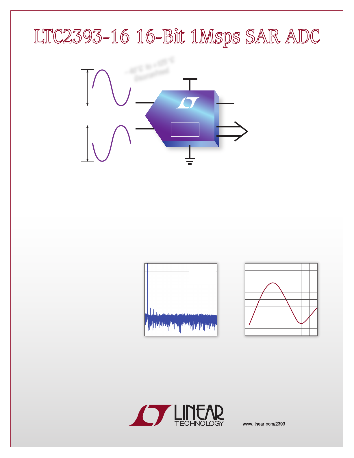
LTC2393-16 16-Bit 1Msps SAR ADC
Wide Fully Differential Input Range Achieves 94.2dB SNR
High SNR is achieved with a ±4.096V maximum signal swing that helps overcome background noise levels in demanding
industrial environments. The LTC2393 features a temperature-compensated internal reference with 0.5% initial accuracy and
20ppm/°C (max) temperature coefficient over the automotive temperature range. The LTC2393-16 dissipates 140mW at 1Msps
and features a shutdown mode that reduces power dissipation to 175µW when not converting. True no latency operation enables
accurate one shot measurements even after idle periods with no minimum sample rate required. To achieve uncompromised AC
performance, we recommend the fast settling LT6350 ADC Driver with rail-to-rail single-ended input and differential outputs.
Features
n
1Msps Throughput Rate
n
±2LSB INL (Max)
n
Guaranteed 16-Bit No Missing Codes
n
94.2dB SNR (Typ) at fIN = 20kHz
n
Single 5V Supply
n
1.8V to 5V I/O Voltages
n
140mW Power Dissipation
n
±4.096V Differential Input Range
n
Internal Reference (10ppm/°C)
n
No Cycle Latency,
16k Point FFT fS = 1Msps
fIN = 20kHz
Internal Reference Output
vs Temperature
One-Shot Operation
n
Parallel and Serial Interface
n
Internal Conversion Clock
n
Pin- and Software-Compatible Versions
500ksps: LTC2392-16
250ksps: LTC2391-16
n
– 40°C to 125°C Operation (LQFP)
n
48-Pin 7mm × 7mm LQFP and QFN Packages
L, LT, LTC, LTM, Linear Technology and the Linear logo are registered
trademarks of Linear Technology Corporation. All other trademarks are the
property of their respective owners.
www.linear.com/2393 n 1-800-4-LINEAR
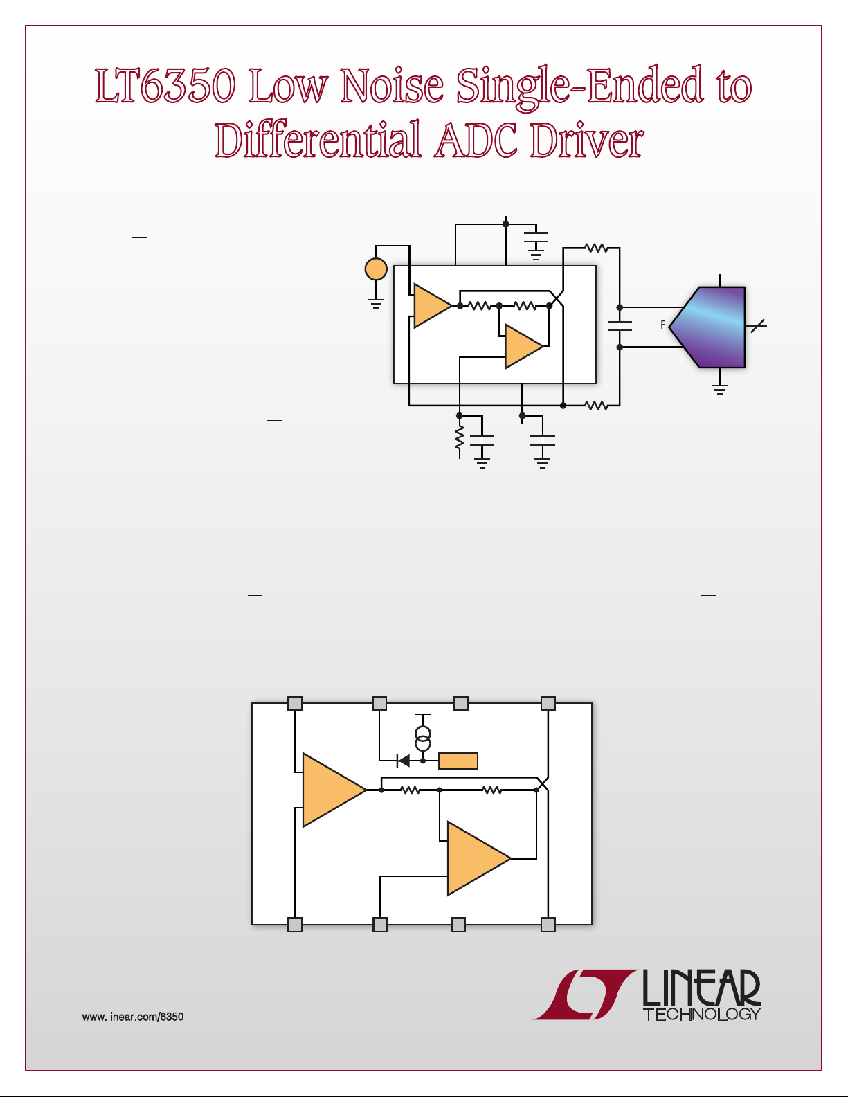
LT6350 Low Noise Single-Ended to
8 6 5
+
IN1
1
–
IN1
V
–
1k1k
3
V
+
OUT2
4
OUT1
SHDN
2
+
IN2
BIAS
7
–
+
+
_
OP AMP 1
OP AMP 2
+
–
+
IN1
–
IN1
V
+
V
–
OUT2
OUT1
SHDN
+
IN2
V
IN
0V to 4V
5V
5V
0.1µF
0.1µF 0.1µF
499Ω
2V
–5V
LT6350
+
–
249Ω
249Ω
2200pF
+
–
A
IN
–
A
IN
+
LTC2393-16
Differential ADC Driver
Features
n
Rail-to-Rail Input and Outputs
n
Fast Settling Time: 240ns, 0.01%, 8V
n
1.9nV/√Hz Input-Referred Op Amp Noise
n
High Impedance Input
n
– 3dB Bandwidth: 33MHz
n
2.7V to 12V Supply Operation
n
No External Gain Resistors Required
n
4.8mA Supply Current
n
Low Power Shutdown
n
Low Distortion (HD2/HD3): –102dBc/–97dBc at
100kHz, V
n
Low Offset Voltage: ±400µV Max
n
High DC Linearity: <±1LSB, 16-Bit, 8V
n
Low Input Current Noise: 1.1pA/√Hz
n
3mm x 3mm 8-Pin DFN and 8-Lead MSOP Packages
OUTDIFF
= 4V
P-P
Output Step
P-P
P-P
Drives High Speed 16- to 18-Bit SAR ADCs
The LT6350 is a 33MHz, low noise, rail-to-rail input and output ADC driver that settles to 16 bits in just 350ns. It is suitable
for driving the latest high performance SAR ADCs like the LTC2393-16. The LT6350 incorporates two op amps and matched
resistors to create a differential output from a single-ended high impedance input. As a result, a differential gain of 2 is achieved
with no external feedback resistors, and higher gain can be obtained by using feedback resistors. Each of the two internal
op amps achieve a low 1.9nV/√Hz input-referred noise density, resulting in a total output referred noise of just 8.2nV/√Hz. The
LT6350 enables high performance ADCs to achieve better than 110dB SNR over a 1MHz bandwidth. Operating from a 2.7V to
12V total supply, the LT6350 consumes 4.8mA supply current and has a shutdown mode that allows the system to reduce power
consumption during periods of inactivity.
www.linear.com/6350 n 1-800-4-LINEAR
 Loading...