

FEATURES
■
Exceeds All Requirements For Full Rate,
Downstream ADSL Line Drivers
■
Power Enhanced 16-Lead SSOP Package
■
Power Saving Adjustable Supply Current
■
±500mA Minimum I
■
±10.9V Output Swing, VS = ±12V, RL = 100Ω
■
±10.7V Output Swing, VS = ±12V, IL = 250mA
■
Low Distortion: –82dBc at 1MHz, 2V
■
200MHz Gain Bandwidth
■
600V/µs Slew Rate
■
Specified at ±12V and ±5V
OUT
P-P
LT6300
500mA, 200MHz xDSL
Line Driver in 16-Lead SSOP Package
U
DESCRIPTIO
The LT®6300 is a 500mA minimum output current, dual op
amp with outstanding distortion performance. The amplifiers are gain-of-ten stable, but can be easily compensated
for lower gains. The extended output swing allows for
lower supply rails to reduce system power. Supply current
is set with an external resistor to optimize power dissipation. The LT6300 features balanced, high impedance in-
Into 50Ω
puts with low input bias current and input offset voltage.
Active termination is easily implemented for further system power reduction. Short-circuit protection and thermal
shutdown insure the device’s ruggedness.
U
APPLICATIO S
■
High Efficiency ADSL, HDSL2, SHDSL Line Drivers
■
Buffers
■
Test Equipment Amplifiers
■
Cable Drivers
U
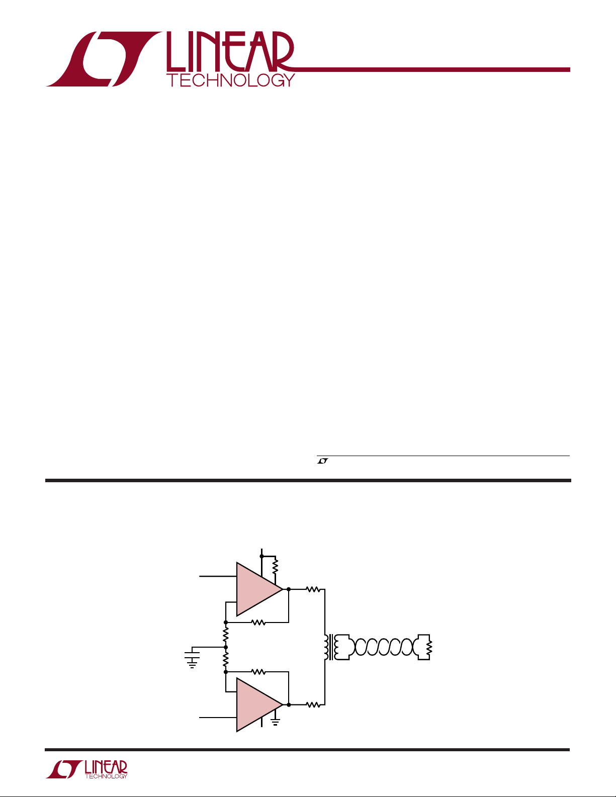
TYPICAL APPLICATIO
High Efficiency ±12V Supply ADSL Line Driver
12V
1000pF
+IN
110Ω
110Ω
+
LT6300
–
1/2
1k
1k
24.9k
SHDN
The outputs drive a 100Ω load to ±10.9V with ±12V
supplies, and ±10.7V with a 250mA load. The LT6300 is a
functional replacement for the LT1739 and LT1794 in
xDSL line driver applications and requires no circuit
changes.
The LT6300 is available in the very small, thermally
enhanced, 16-lead SSOP package (same PCB area as the
SO-8 package) for maximum port density in line driver
applications.
, LTC and LT are registered trademarks of Linear Technology Corporation.
12.7Ω
1:2*
•
•
100Ω
–IN
–
LT6300
+
1/2
–12V
SHDNREF
12.7Ω
*COILCRAFT X8390-A OR EQUIVALENT
= 10mA PER AMPLIFIER
I
SUPPLY
WITH R
SHDN
= 24.9k
6300 TA01
1
LT6300
WW
W
ABSOLUTE MAXIMUM RATINGS
U
U
W
PACKAGE/ORDER INFORMATION
(Note 1)
Supply Voltage (V+ to V–) ................................. ±13.5V
Input Current ..................................................... ±10mA
Output Short-Circuit Duration (Note 2)........... Indefinite
Operating Temperature Range ............... – 40°C to 85°C
Specified Temperature Range (Note 3).. – 40°C to 85°C
Junction Temperature.......................................... 150°C
Storage Temperature Range ................. –65°C to 150°C
Lead Temperature (Soldering, 10 sec).................. 300°C
V
–IN
+IN
SHDN
SHDNREF
+IN
–IN
V
T
= 150°C, θJA = 70°C/W to 95°C/W (Note 4)
JMAX
Consult LTC Marketing for parts specified with wider operating temperature
ranges.
TOP VIEW
–
1
2
3
4
5
6
7
–
8
GN PACKAGE
16-LEAD PLASTIC SSOP
ORDER PART
–
16
V
15
OUT
14
NC
+
13
V
+
12
V
11
NC
10
OUT
–
9
V
NUMBER
LT6300CGN
LT6300IGN
GN PART
MARKING
6300
6300I
ELECTRICAL CHARACTERISTICS
The ● denotes the specifications which apply over the full specified temperature range, otherwise specifications are at TA = 25°C.
VCM = 0V, pulse tested, ±5V ≤ VS ≤ ±12V, V
SHDNREF
= 0V, R
= 24.9k between V+ and SHDN unless otherwise noted. (Note 3)
BIAS
U
SYMBOL PARAMETER CONDITIONS MIN TYP MAX UNITS
V
OS
I
OS
I
B
e
n
i
n
R
IN
C
IN
CMRR Common Mode Rejection Ratio V
PSRR Power Supply Rejection Ratio VS = ±4V to ±12V 74 88 dB
Input Offset Voltage 15.0 mV
● 7.5 mV
Input Offset Voltage Matching 0.3 5.0 mV
● 7.5 mV
Input Offset Voltage Drift ● 10 µV/°C
Input Offset Current 100 500 nA
● 800 nA
Input Bias Current ±0.1 ±4 µA
● ±6 µA
Input Bias Current Matching 100 500 nA
● 800 nA
Input Noise Voltage Density f = 10kHz 8 nV/√Hz
Input Noise Current Density f = 10kHz 0.8 pA/√Hz
Input Resistance V
Input Capacitance 3pF
Input Voltage Range (Positive) (Note 5) ● V+ – 2 V+ – 1 V
Input Voltage Range (Negative) (Note 5)
= (V+ – 2V) to (V–+ 2V) ● 550 MΩ
CM
Differential 6.5 MΩ
● V
= (V+ – 2V) to (V– + 2V) 74 83 dB
CM
● 66 dB
● 66 dB
–
+ 1 V– + 2 V
2
LT6300
ELECTRICAL CHARACTERISTICS
The ● denotes the specifications which apply over the full specified temperature range, otherwise specifications are at TA = 25°C.
VCM = 0V, pulse tested, ±5V ≤ VS ≤ ±12V, V
SHDNREF
SYMBOL PARAMETER CONDITIONS MIN TYP MAX UNITS
A
V
I
I
VOL
OUT
OUT
S
Large-Signal Voltage Gain VS = ±12V, V
Output Swing VS = ±12V, RL = 100Ω 10.7 10.9 ±V
Maximum Output Current VS = ±12V, RL = 1Ω 500 1200 mA
Supply Current per Amplifier VS = ±12V, R
Supply Current in Shutdown V
Output Leakage in Shutdown V
Channel Separation VS = ±12V, V
SR Slew Rate VS = ±12V, AV = –10, (Note 7) 300 600 V/µs
HD2 Differential 2nd Harmonic Distortion VS = ±12V, AV = 10, 2V
HD3 Differential 3rd Harmonic Distortion VS = ±12V, AV = 10, 2V
GBW Gain Bandwidth f = 1MHz 200 MHz
= 0V, R
VS = ±5V, V
= 24.9k between V+ and SHDN unless otherwise noted. (Note 3)
BIAS
= ±10V, RL = 40Ω 63 76 dB
OUT
= ±3V, RL = 25Ω 60 70 dB
OUT
● 57 dB
● 54 dB
● 10.5 ±V
VS = ±12V, IL = 250mA 10.4 10.7 ±V
● 10.2 ±V
VS = ±5V, RL = 25Ω 3.5 3.8 ±V
● 3.3 ±V
VS = ±5V, IL = 250mA 3.4 3.7 ±V
● 3.2 ±V
= 24.9k (Note 6) 8.0 10 13.5 mA
BIAS
= ±12V, R
V
S
= ±12V, R
V
S
VS = ±12V, R
VS = ±5V, R
= 0.4V 0.1 1 mA
SHDN
= 0.4V 0.3 1 mA
SHDN
= 32.4k (Note 6) 8 mA
BIAS
= 43.2k (Note 6) 6 mA
BIAS
= 66.5k (Note 6) 4 mA
BIAS
= 24.9k (Note 6) 2.2 3.4 5.0 mA
BIAS
= ±10V, RL = 40Ω 80 110 dB
OUT
● 6.7 15.0 mA
● 1.8 5.8 mA
● 77 dB
VS = ±5V, AV = –10, (Note 7) 100 200 V/µs
, RL = 50Ω, 1MHz –85 dBc
P-P
, RL = 50Ω, 1MHz –82 dBc
P-P
Note 1: Absolute Maximum Ratings are those values beyond which the life
of a device may be impaired.
Note 2: Applies to short circuits to ground only. A short circuit between
the output and either supply may permanently damage the part when
operated on supplies greater than ±10V.
Note 3: The LT6300C is guaranteed to meet specified performance from
0°C to 70°C and is designed, characterized and expected to meet these
extended temperature limits, but is not tested at –40°C and 85°C. The
LT6300I is guaranteed to meet the extended temperature limits.
Note 4: Thermal resistance varies depending upon the amount of PC board
metal attached to Pins 1, 8, 9, 16 of the device. If the maximum
dissipation of the package is exceeded, the device will go into thermal
shutdown and be protected.
Note 5: Guaranteed by the CMRR tests.
Note 6: R
is connected between V+ and the SHDN pin, with the
BIAS
SHDNREF pin grounded.
Note 7: Slew rate is measured at ±5V on a ±10V output signal while
operating on ±12V supplies and ±1V on a ±3V output signal while
operating on ±5V supplies.
3
LT6300
TEMPERATURE (°C)
–50
OUTPUT SATURATION VOLTAGE (V)
–0.5
10
6300 G06
1.0
–30 –10 30
0.5
V
–
V
+
–1.0
–1.5
1.5
50 70 90
VS = ±12V
RL = 100Ω
RL = 100Ω
I
LOAD
= 250mA
I
LOAD
= 250mA
UW
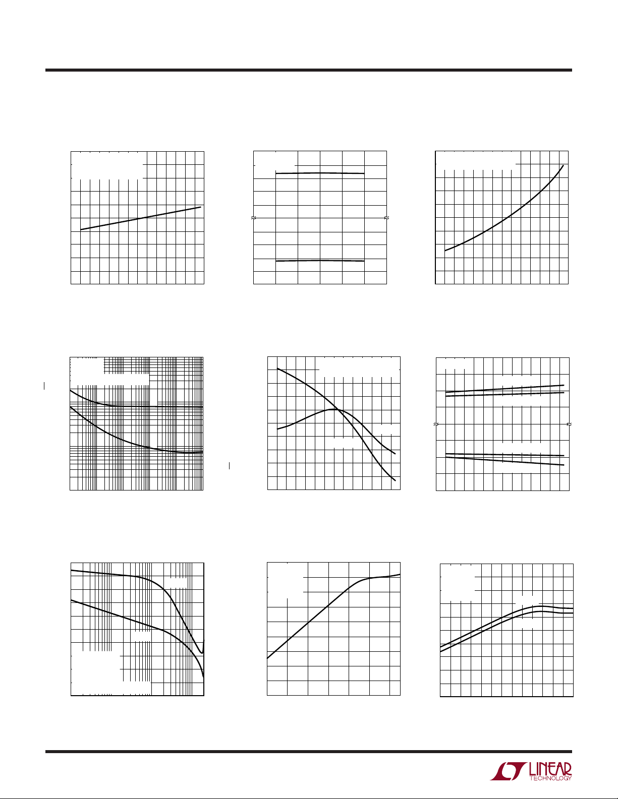
TYPICAL PERFOR A CE CHARACTERISTICS
Supply Current
vs Ambient Temperature
15
VS = ±12V
14
= 24.9k TO SHDN
R
BIAS
= 0V
V
SHDNREF
13
12
11
10
9
PER AMPLIFIER (mA)
8
SUPPLY
I
7
6
5
–30 –10 10 30 50 70 90
–50
TEMPERATURE (°C)
Input Noise Spectral Density
100
TA = 25°C
V
= ±12V
S
PER AMPLIFIER = 10mA
I
S
10
1
INPUT VOLTAGE NOISE (V/√Hz)
0.1
10
1 100 1k 10k
FREQUENCY (Hz)
Input Common Mode Range
vs Supply Voltage
+
V
TA = 25°C
> 1mV
∆V
–0.5
OS
–1.0
–1.5
–2.0
2.0
1.5
COMMON MODE RANGE (V)
1.0
0.5
–
6300 G01
V
2
4
SUPPLY VOLTAGE (±V)
6
810
12
14
6300 G02
Output Short-Circuit Current
vs Ambient Temperature
INPUT CURRENT NOISE (pA/√Hz)
800
780
760
740
720
700
(mA)
SC
I
680
660
640
600
620
–50
VS = ±12V
I
–30 10
–10
TEMPERATURE (°C)
PER AMPLIFIER = 10mA
S
SINKING
SOURCING
30
70
50
90
6300 G05
100
e
n
i
n
6300 G04
100k
10
1
0.1
Input Bias Current
vs Ambient Temperature
200
VS = ±12V
180
PER AMPLIFIER = 10mA
I
S
160
140
120
(nA)
100
BIAS
±I
80
60
40
20
0
–50
–30
10 30
–10
TEMPERATURE (°C)
Output Saturation Voltage
vs Ambient Temperature
50
70 90
6300 G03
Open-Loop Gain and Phase
vs Frequency
120
100
80
60
40
20
GAIN (dB)
0
–20
–40
–60
–80
100k 10M 100M
4
TA = 25°C
= ±12V
V
S
= –10
A
V
= 100Ω
R
L
PER AMPLIFIER = 10mA
I
S
1M
GAIN
FREQUENCY (Hz)
PHASE
6300 G07
120
80
40
0
–40
–80
–120
–160
–200
–240
–280
45
40
35
30
PHASE (DEG)
25
20
15
–3dB BANDWIDTH (MHz)
10
5
0
–3dB Bandwidth
vs Supply Current Slew Rate vs Supply Current
TA = 25°C
V
= ±12V
S
= 10
A
V
R
= 100Ω
L
4
2
SUPPLY CURRENT PER AMPLIFIER (mA)
6 8 10 12 14
6300 G08
1000
TA = 25°C
900
= ±12V
V
S
= –10
A
V
800
R
= 1k
L
700
600
500
400
SLEW RATE (V/µs)
300
200
100
0
345
2
SUPPLY CURRENT PER AMPLIFIER (mA)
67
8910
RISING
FALLING
11 12
13 14
6300 G09
15
UW
TYPICAL PERFOR A CE CHARACTERISTICS
CMRR vs Frequency PSRR vs Frequency
100
90
80
70
60
50
40
30
20
10
COMMON MODE REJECTION RATIO (dB)
0
0.1
TA = 25°C
= ±12V
V
S
= 10mA PER AMPLIFIER
I
S
1 10 100
FREQUENCY (MHz)
6300 G10
100
90
80
70
60
50
40
30
20
10
POWER SUPPLY REJECTION (dB)
0
–10
0.01 1 10 100
VS = ±12V
= 10
A
V
= 10mA PER AMPLIFIER
I
S
(–) SUPPLY
(+) SUPPLY
0.1
FREQUENCY (MHz)
6300 G11
Frequency Response
vs Supply Current
30
VS = ±12V
25
= 10
A
V
20
15
10
5
GAIN (dB)
0
–5
–10
–15
–20
1k 10k
2mA PER AMPLIFIER
10mA PER AMPLIFIER
15mA PER AMPLIFIER
LT6300
100k 1M 10M 100M
FREQUENCY (Hz)
6300 G12
Output Impedance vs Frequency I
1000
TA = 25°C
±12V
V
S
100
IS PER
IS PER
IS PER
AMPLIFIER = 15mA
1 10 100
FREQUENCY (MHz)
6300 G13
10
AMPLIFIER = 10mA
1
OUTPUT IMPEDANCE (Ω)
0.1
0.01
0.01 0.1
AMPLIFIER = 2mA
Differential Harmonic Distortion
vs Output Amplitude
–40
f = 1MHz
T
= 25°C
A
–50
V
= ±12V
S
= 10
A
V
R
= 50Ω
L
–60
I
PER AMPLIFIER = 10mA
S
–70
–80
DISTORTION (dBc)
–90
–100
02
6
4 8 10 12 14 16 18
V
OUT(P-P)
HD3
HD2
2.5
2.0
1.5
(mA)
SHDN
I
1.0
0.5
0
0
6300 G16
SHDN
TA = 25°C
= ±12V
V
S
V
SHDNREF
0.5
vs V
= 0V
1.0
SHDN
1.5
2.0
V
2.5
SHDN
(V)
3.0
3.5
4.0
4.5
6300 G14
DISTORTION (dBc)
Supply Current vs V
35
TA = 25°C
= ±12V
V
S
5.0
30
25
20
15
10
5
SUPPLY CURRENT PER AMPLIFIER (mA)
0
0
V
SHDNREF
0.5
1.0
= 0V
1.5
2.0
V
SHDN
Differential Harmonic Distortion
vs Frequency
–40
VO = 10V
–45
–50
–55
–60
–65
–70
–75
–80
–85
–90
P-P
TA = 25°C
= ±12V
V
S
A
= 10
V
R
= 50Ω
L
PER AMPLIFIER = 10mA
I
S
200100
400300
500
FREQUENCY (kHz)
HD3
600 700 900
2.5
800
3.0
(V)
HD2
SHDN
6300 G17
3.5
1000
4.0
4.5
6300 G15
5.0
5

LT6300
UW
TYPICAL PERFOR A CE CHARACTERISTICS
Differential Harmonic Distortion
vs Supply Current
–40
–45
–50
–55
–60
–65
–70
DISTORTION (dBc)
–75
–80
–85
23456 11
I
SUPPLY
TEST CIRCUIT
f = 1MHz, HD3
f = 100kHz, HD2
f = 100kHz, HD3
f = 1MHz, HD2
78910
PER AMPLIFIER (mA)
VO = 10V
VS = ±12V
= 10
A
V
= 50Ω
R
L
6300 G18
10k
P-P
Undistorted Output Swing
vs Frequency
20
)
15
P-P
10
SFDR > 40dB
= 25°C
T
A
5
OUTPUT VOLTAGE (V
= ±12V
V
S
= 10
A
V
= 50Ω
R
L
PER AMPLIFIER = 10mA
I
S
0
100k
12V
R
BIAS
12
13
3
+
2
–
–12V
4 (SHDN)
A
16
1
1k
V
OUT(P-P)
15
12.7Ω
1:2*
300k 1M 3M 10M
FREQUENCY (Hz)
6300 G19
SUPPLY BYPASSING
+
0.1µF 4.7µF
+
0.1µF
4.7µF
+
4.7µF
12V
0.1µF
–12V
6
OUT (+)
E
IN
49.9Ω
SPLITTER
MINICIRCUITS
ZSC5-2-2
OUT (–)
10k
110Ω
110Ω
7
6
–12V
R
≈ 50Ω
L
0.01µF
1k
–
B
+
9
8
10
5 (SHDNREF)
12.7Ω
6300 TC
*COILCRAFT X8390-A OR EQUIVALENT
AMPLITUDE SET AT EACH AMPLIFIER OUTPUT
V
OUTP-P
DISTORTION MEASURED ACROSS LINE LOAD
100 LINE LOAD

WUUU
APPLICATIO S I FOR ATIO
LT6300
The LT6300 is a high speed, 200MHz gain bandwidth
product, dual voltage feedback amplifier with high output
current drive capability, 500mA source and sink. The
LT6300 is ideal for use as a line driver in xDSL data
communication applications. The output voltage swing
has been optimized to provide sufficient headroom when
operating from ±12V power supplies in full-rate ADSL
applications. The LT6300 also allows for an adjustment of
the operating current to minimize power consumption. In
addition, the LT6300 is available in a small footprint
surface mount package to minimize PCB area.
To minimize signal distortion, the LT6300 amplifiers are
decompensated to provide very high open-loop gain at
high frequency. As a result each amplifier is frequency
stable with a closed-loop gain of 10 or more. If a closedloop gain of less than 10 is desired, external frequency
compensating components can be used.
SHDN
5I
2k
Setting the Quiescent Operating Current
Power consumption and dissipation are critical concerns
in multiport xDSL applications. Two pins, Shutdown
(SHDN) and Shutdown Reference (SHDNREF), are provided to control quiescent power consumption and allow
for the complete shutdown of the driver. The quiescent
current should be set high enough to prevent distortion
induced errors in a particular application, but not so high
that power is wasted in the driver unnecessarily. A good
starting point to evaluate the LT6300 is to set the quiescent
current to 10mA per amplifier.
The internal biasing circuitry is shown in Figure 1. Grounding the SHDNREF pin and directly driving the SHDN pin with
a voltage can control the operating current as seen in the
Typical Performance Characteristics. When the SHDN pin
is less than SHDNREF + 0.4V, the driver is shut down and
consumes typically only 100µA of supply current and the
outputs are in a high impedance state. Part to part variations, however, will cause inconsistent control of the quiescent current if direct voltage drive of the SHDN pin is used.
I
TO
START-UP
CIRCUITRY
SHDNREF
2
I
=
I
BIAS
SHDN
5
PER AMPLIFIER (mA) = 64 • I
I
SUPPLY
= I
SHDNREF
2I
2I
1k
I
BIAS
TO AMPLIFIERS
BIAS CIRCUITRY
6300 F01
BIAS
Figure 1. Internal Current Biasing Circuitry
30
VS = ±12V
25
20
15
PER AMPLIFIER (mA)
10
SUPPLY
I
5
0
7 40 70 100 130 160 190
10
Figure 2. R
Using a single external resistor, R
two ways provides a much more predictable control of the
quiescent supply current. Figure 2 illustrates the effect on
supply current per amplifier with R
tween the SHDN pin and the 12V V+ supply of the LT6300
and the approximate design equations. Figure 3 illustrates
the same control with R
SHDNREF pin and ground while the SHDN pin is tied to V+.
Either approach is equally effective.
V+ = 12V
R
BIAS
SHDN
PER AMPLIFIER
I
S
R
=
BIAS
I
SHDNREF
R
(kΩ)
BIAS
to V+ Current Control
BIAS
≈
(mA)
+
V
– 1.2V
PER AMPLIFIER (mA)
S
V
R
BIAS
+
– 1.2V
+ 2k
• 25.6
• 25.6 – 2k
6300 F02
, connected in one of
BIAS
connected be-
BIAS
connected between the
BIAS
7

LT6300
WUUU
APPLICATIO S I FOR ATIO
45
VS = ±12V
40
35
30
25
20
PER AMPLIFIER (mA)
15
SUPPLY
10
I
5
0
4 7 10 50 90 130 170 210 25030 70 100 150 190 230 270 290
Figure 3. R
BIAS
V+ = 12V
SHDN
PER AMPLIFIER
I
S
R
=
BIAS
SHDNREF
R
BIAS
R
(kΩ)
BIAS
(mA)
+
V
– 1.2V
PER AMPLIFIER (mA)
I
S
to Ground Current Control
V
≈
R
Two Control Inputs
RESISTOR VALUES (kΩ)
TO V
3.3V
43.2
13.0
22.1
10
7
5
2
(12V) R
CC
60.4
21.5
36.5
5V
10
7
5
2
R
SHDN
V
3V
LOGIC
R
40.2
SHDN
R
11.5
C1
R
19.1
V
CO
V
SUPPLY CURRENT PER AMPLIFIER (mA)
C0
C1
H
H
H
L
L
10
L
7
H
5
L
2
3V
4.99
8.66
14.3
10
SHDN
7
5
2
TO V
3.3V
6.81
10.7
17.8
10
7
5
2
LOGIC
5V
19.6
20.5
34.0
10
7
5
2
V
LOGIC
R
C1
V
C1
R
0V
C0
V
C0
One Control Input
RESISTOR VALUES (kΩ)
TO V
3.3V
43.2
8.25
(12V) R
CC
60.4
13.7
5V
R
SHDN
V
3V
LOGIC
R
40.2
SHDN
R
7.32
C
V
SUPPLY CURRENT PER AMPLIFIER (mA)
C
HL10210210210210210
3V
4.99
5.49
SHDN
TO V
3.3V
6.81
6.65
LOGIC
5V
19.6
12.7
2
6300 F04
V
LOGIC
R
C
V
0V
C
+
– 1.2V
+ 5k
BIAS
• 64 – 5k
12V OR V
12V OR V
• 64
6300 F03
LOGIC
R
SHDN
SHDN
2k
SHDNREF
LOGIC
R
SHDN
SHDN
2k
SHDNREF
Figure 4. Providing Logic Input Control of Operating Current
Logic Controlled Operating Current
The DSP controller in a typical xDSL application can have
I/O pins assigned to provide logic control of the LT6300
line driver operating current. As shown in Figure 4 one or
two logic control inputs can control two or four different
operating modes. The logic inputs add or subtract current
to the SHDN input to set the operating current. The one
logic input example selects the supply current to be either
full power, 10mA per amplifier or just 2mA per amplifier,
which significantly reduces the driver power consumption
8
while maintaining less than 2Ω output impedance to
frequencies less than 1MHz. This low power mode retains
termination impedance at the amplifier outputs and the
line driving back termination resistors. With this termination, while a DSL port is not transmitting data, it can still
sense a received signal from the line across the backtermination resistors and respond accordingly.
The two logic input control provides two intermediate
(approximately 7mA per amplifier and 5mA per amplifier)
operating levels between full power and termination

WUUU
APPLICATIO S I FOR ATIO
LT6300
modes. These modes can be useful for overall system
power management when full power transmissions are
not necessary.
Shutdown and Recovery
The ultimate power saving action on a completely idle port
is to fully shut down the line driver by pulling the SHDN pin
to within 0.4V of the SHDNREF potential. As shown in
Figure 5 complete shutdown occurs in less than 10µs and,
more importantly, complete recovery from the shut down
state to full operation occurs in less than 2µs. The biasing
circuitry in the LT6300 reacts very quickly to bring the
amplifiers back to normal operation.
V
SHDN
SHDNREF = 0V
AMPLIFIER
OUTPUT
Power Dissipation and Heat Management
xDSL applications require the line driver to dissipate a
significant amount of power and heat compared to other
components in the system. The large peak to RMS variations of DMT and CAP ADSL signals require high supply
voltages to prevent clipping, and the use of a step-up
transformer to couple the signal to the telephone line can
require high peak current levels. These requirements
result in the driver package having to dissipate significant
amounts of power. Several multiport cards inserted into
a rack in an enclosed central office box can add up to
many, many watts of power dissipation in an elevated
ambient temperature environment. The LT6300 has builtin thermal shutdown cir
cuitry that will protect the amplifiers if operated at excessive temperatures, however data
transmissions will be seriously impaired. It is important in
the design of the PCB and card enclosure to take measures
to spread the heat developed in the driver away to the
ambient environment to prevent thermal shutdown (which
occurs when the junction temperature of the LT6300
exceeds 165°C).
6300 F05
Figure 5. Shutdown and Recovery Timing
12V
24.9k – SETS I
2V
SHDN
A
+IN
20mA DC
+
–
1k
110Ω
I
1000pF
110Ω
LOAD
1k
–
B
–IN
+
SHDNREF
–12V
–2V
RMS
= 57mA
RMS
PER AMPLIFIER = 10mA
Q
17.4Ω
1:1.7
•
•
RMS
17.4Ω
6300 F06
Estimating Line Driver Power Dissipation
Figure 6 is a typical ADSL application shown for the
purpose of estimating the power dissipation in the line
driver. Due to the complex nature of the DMT signal,
100Ω 3.16V
RMS
Figure 6. Estimating Line Driver Power Dissipation
9

LT6300
WUUU
APPLICATIO S I FOR ATIO
which looks very much like noise, it is easiest to use the
RMS values of voltages and currents for estimating the
driver power dissipation. The voltage and current levels
shown for this example are for a full-rate ADSL signal
driving 20dBm or 100mW
of power on to the 100Ω
RMS
telephone line and assuming a 0.5dBm insertion loss in
the transformer. The quiescent current for the LT6300 is
set to 10mA per amplifier.
The power dissipated in the LT6300 is a combination of the
quiescent power and the output stage power when driving
a signal. The two amplifiers are configured to place a
differential signal on to the line. The Class AB output stage
in each amplifier will simultaneously dissipate power in
the upper power transistor of one amplifier, while sourcing current, and the lower power transistor of the other
amplifier, while sinking current. The total device power
dissipation is then:
PD = P
QUIESCENT
PD = (V+ – V–) • IQ + (V+ – V
I
LOAD
+ P
+ (V– – V
Q(UPPER)
OUTBRMS
+ P
Q(LOWER)
OUTARMS
) • I
LOAD
) •
With no signal being placed on the line and the amplifier
biased for 10mA per amplifier supply current, the quiescent driver power dissipation is:
PDQ = 24V • 20mA = 480mW
This can be reduced in many applications by operating
with a lower quiescent current value.
When driving a load, a large percentage of the amplifier
quiescent current is diverted to the output stage and
becomes part of the load current. Figure 7 illustrates the
total amount of biasing current flowing between the + and
– power supplies through the amplifiers as a function of
load current. As much as 60% of the quiescent no load
operating current is diverted to the load.
At full power to the line the driver power dissipation is:
P
D(FULL)
P
D(FULL)
= 24V • 8mA + (12V – 2V
+ [|–12V – (–2V
)|] • 57mA
RMS
RMS
) • 57mA
RMS
RMS
= 192mW + 570mW + 570mW = 1.332W
The junction temperature of the driver must be kept less
than the thermal shutdown temperature when processing
a signal. The junction temperature is determined from the
following expression:
TJ = T
AMBIENT
(°C) + P
D(FULL)
(W) • θJA (°C/W)
θJA is the thermal resistance from the junction of the
LT6300 to the ambient air, which can be minimized by
heat-spreading PCB metal and airflow through the enclosure as required. For the example given, assuming a
maximum ambient temperature of 50°C and keeping the
junction temperature of the LT6300 to 150°C maximum,
the maximum thermal resistance from junction to ambient
required is:
CC
–
°°
θ
JA MAX
()
150 50
W
.
1 332
CW
./=
=°
75 1
10
25
20
15
(mA)
Q
10
TOTAL I
5
0
–240 –200 –160 –120 –80 –40 0 40 80 120 160 200 240
I
(mA)
LOAD
Figure 7. IQ vs I
LOAD
6300 F07

WUUU
APPLICATIO S I FOR ATIO
LT6300
Heat Sinking Using PCB Metal
Designing a thermal management system is often a trial
and error process as it is never certain how effective it is
until it is manufactured and evaluated. As a general rule,
the more copper area of a PCB used for spreading heat
away from the driver package, the more the operating
junction temperature of the driver will be reduced. The
limit to this approach however is the need for very compact circuit layout to allow more ports to be implemented
on any given size PCB.
To best extract heat from the GN16 package, a generous
area of top layer PCB metal should be connected to the four
corner pins (Pins 1, 8, 9 and 16). These pins are fused to
the leadframe where the LT6300 die is attached. It is
important to note that this heat spreading metal area is
electrically connected to the V– supply voltage.
Fortunately xDSL circuit boards use multiple layers of
metal for interconnection of components. Areas of metal
beneath the LT6300 connected together through several
small 13 mil vias can be effective in conducting heat away
from the driver package. The use of inner layer metal can
free up top and bottom layer PCB area for external component placement.
When PCB cards containing multiple ports are inserted
into a rack in an enclosed cabinet, it is often necessary to
provide airflow through the cabinet and over the cards.
This is also very effective in reducing the junction-toambient thermal resistance of each line driver. To a limit,
this thermal resistance can be reduced approximately
5°C/W for every 100lfpm of laminar airflow.
the input capacitance to form a pole that can cause
frequency peaking. In general, use feedback resistors of
1k or less.
Compensation
The LT6300 is stable in a gain 10 or higher for any supply
and resistive load. It is easily compensated for lower gains
with a single resistor or a resistor plus a capacitor.
Figure␣ 8 shows that for inverting gains, a resistor from the
inverting node to AC ground guarantees stability if the
parallel combination of RC and RG is less than or equal to
RF/9. For lowest distortion and DC output offset, a series
capacitor, CC, can be used to reduce the noise gain at
lower frequencies. The break frequency produced by R
C
and CC should be less than 5MHz to minimize peaking.
Figure 9 shows compensation in the noninverting configu-
ration. The RC, CC network acts similarly to the inverting
case. The input impedance is not reduced because the
network is bootstrapped. This network can also be placed
between the inverting input and an AC ground.
R
F
–R
V
F
O
O
=
R
V
G
I
(RC || RG) ≤ RF/9
1
< 5MHz
2πR
CCC
6300 F08
R
V
I
(OPTIONAL)
G
R
C
C
C
–
+
Figure 8. Compensation for Inverting Gains
V
Layout and Passive Components
With a gain bandwidth product of 200MHz the LT6300
requires attention to detail in order to extract maximum
performance. Use a ground plane, short lead lengths and
a combination of RF-quality supply bypass capacitors (i.e.,
0.1µF). As the primary applications have high drive cur-
rent, use low ESR supply bypass capacitors (1µF to 10µF).
The parallel combination of the feedback resistor and gain
setting resistor on the inverting input can combine with
V
O
V
V
(RC || RG) ≤ RF/9
2πR
V
(OPTIONAL)
I
R
C
C
C
R
G
+
–
R
F
Figure 9. Compensation for Noninverting Gains
R
= 1 +
1
CCC
F
R
G
< 5MHz
6300 F09
O
I
11

LT6300
WUUU
APPLICATIO S I FOR ATIO
Another compensation scheme for noninverting circuits is
shown in Figure 10. The circuit is unity gain at low frequency and a gain of 1 + RF/RG at high frequency. The DC
output offset is reduced by a factor of ten. The techniques
of Figures 9 and 10 can be combined as shown in Figure␣ 11. The gain is unity at low frequencies, 1 + RF/RG at
mid-band and for stability, a gain of 10 or greater at high
frequencies.
In differential driver applications, as shown on the first
page of this data sheet, it is recommended that the gain
setting resistor be comprised of two equal value resistors
connected to a good AC ground at high frequencies. This
ensures that the feedback factor of each amplifier remains
less than 0.1 at any frequency. The midpoint of the
resistors can be directly connected to ground, with the
resulting DC gain to the VOS of the amplifiers, or just
bypassed to ground with a 1000pF or larger capacitor.
Line Driving Back-Termination
The standard method of cable or line back-termination is
shown in Figure 12. The cable/line is terminated in its
characteristic impedance (50Ω, 75Ω, 100Ω, 135Ω, etc.).
V
+
V
i
–
R
F
R
G
C
C
Figure 10. Alternate Noninverting Compensation
V
I
R
C
C
C
R
G
C
BIG
+
–
R
F
O
= 1 (LOW FREQUENCIES)
V
I
R
F
(HIGH FREQUENCIES)
= 1 +
V
O
V
O
V
O
V
I
R
G
RG ≤ RF/9
1
< 5MHz
2πR
GCC
= 1 AT LOW FREQUENCIES
R
F
= 1 + AT MEDIUM FREQUENCIES
R
G
R
= 1 + AT HIGH FREQUENCIES
F
(RC || RG)
6300 F10
6300 F11
A back-termination resistor also equal to the chararacteristic
impedance should be used for maximum pulse fidelity of
outgoing signals, and to terminate the line for incoming
signals in a full-duplex application. There are three main
drawbacks to this approach. First, the power dissipated in
the load and back-termination resistors is equal so half of
the power delivered by the amplifier is wasted in the
termination resistor. Second, the signal is halved so the
gain of the amplifer must be doubled to have the same
overall gain to the load. The increase in gain increases
noise and decreases bandwidth (which can also increase
distortion). Third, the output swing of the amplifier is
doubled which can limit the power it can deliver to the load
for a given power supply voltage.
An alternate method of back-termination is shown in
Figure 13. Positive feedback increases the effective backtermination resistance so RBT can be reduced by a factor
CABLE OR LINE WITH
+
V
I
CHARACTERISTIC IMPEDANCE R
R
BT
–
R
F
R
G
RBT = R
V
O
=
V
I
L
1
(1 + RF/RG)
2
Figure 12. Standard Cable/Line Back Termination
R
P2
R
P1
V
I
+
R
V
BT
V
P
–
R
F
R
G
FOR RBT =
R
F
1 +
R
()
G
V
O
=
V
I
()
A
R
R
L
n
P2
–
= 1 –
R
P1
RP2 + R
1
n
P1
R
P1
RP1 + R
()
RP2/(RP2 + RP1)
1 + 1/n
R
F
1 +
R
G
L
V
O
R
L
6300 F12
V
O
L
6300 F13
12
Figure 11. Combination Compensation
Figure 13. Back Termination Using Postive Feedback

WUUU
APPLICATIO S I FOR ATIO
LT6300
of n. To analyze this circuit, first ground the input. As RBT␣=
RL/n, and assuming RP2>>RL we require that:
VA = VO (1 – 1/n) to increase the effective value of
RBT by n.
VP = VO (1 – 1/n)/(1 + RF/RG)
VO = VP (1 + RP2/RP1)
Eliminating VP, we get the following:
(1 + RP2/RP1) = (1 + RF/RG)/(1 – 1/n)
For example, reducing RBT by a factor of n = 4, and with an
amplifer gain of (1 + RF/RG) = 10 requires that RP2/R
P1
=␣ 12.3.
Note that the overall gain is increased:
/
V
O
=
V
I
+
11 1
()
[]
RRR
221
PPP
// / /
+
nRRRRR
()
FG P P P
+
()
−+
()
[]
12 1
A simpler method of using positive feedback to reduce the
back-termination is shown in Figure 14. In this case, the
drivers are driven differentially and provide complementary outputs. Grounding the inputs, we see there is inverting gain of –RF/RP from –VO to V
A
VA = VO (RF/RP)
and assuming RP >> RL, we require
VA = VO (1 – 1/n)
solving
RF/RP = 1 – 1/n
So to reduce the back-termination by a factor of 3 choose
RF/RP = 2/3. Note that the overall gain is increased to:
VO/VI = (1 + RF/RG + RF/RP)/[2(1 – RF/RP)]
Using positive feedback is often referred to as active
termination.
Figure 16 shows a full-rate ADSL line driver incorporating
positive feedback to reduce the power lost in the back
termination resistors by 40% yet still maintains the proper
impedance match to the100Ω characteristic line impedance. This circuit also reduces the transformer turns ratio
over the standard line driving approach resulting in lower
peak current requirements. With lower current and less
power loss in the back termination resistors, this driver
dissipates only 1W of power, a 30% reduction.
While the power savings of positive feedback are attractive
there is one important system consideration to be addressed, received signal sensitivity. The signal received
from the line is sensed across the back termination resistors. With positive feedback, signals are present on both
ends of the RBT resistors, reducing the sensed amplitude.
Extra gain may be required in the receive channel to
compensate, or a completely separate receive path may be
implemented through a separate line coupling transformer.
V
+
I
–
R
G
R
R
R
G
–
+
–V
I
Figure 14. Back Termination Using Differential Postive Feedback
V
R
A
BT
R
F
P
P
R
F
R
BT
–V
A
6300 F14
V
O
R
L
=
FOR R
BT
n
1
n =
R
F
–V
1 –
R
P
R
R
F
F
+
1 +
R
V
O
=
V
I
O
R
G
P
R
F
1 –2
R
()
P
R
L
R
L
Considerations for Fault Protection
The basic line driver design, shown on the front page of
this data sheet, presents a direct DC path between the
outputs of the two amplifiers. An imbalance in the DC
biasing potentials at the noninverting inputs through
either a fault condition or during turn-on of the system can
create a DC voltage differential between the two amplifier
outputs. This condition can force a considerable amount
of current to flow as it is limited only by the small valued
back-termination resistors and the DC resistance of the
transformer primary. This high current can possibly cause
the power supply voltage source to drop significantly
impacting overall system performance. If left unchecked,
the high DC current can heat the LT6300 to thermal
shutdown.
13

LT6300
WUUU
APPLICATIO S I FOR ATIO
Using DC blocking capacitors, as shown in Figure 15, to
AC couple the signal to the transformer eliminates the
possibility for DC current to flow under any conditions.
These capacitors should be sized large enough to not
impair the frequency response characteristics required for
the data transmission.
Another important fault related concern has to do with
very fast high voltage transients appearing on the telephone line (lightning strikes for example). TransZorbs®,
varistors and other transient protection devices are often
used to absorb the transient energy, but in doing so also
12V
1000pF
+IN
110Ω
110Ω
+
LT6300
–
1/2
SHDN
1k
1k
create fast voltage transitions themselves that can be
coupled through the transformer to the outputs of the line
driver. Several hundred volt transient signals can appear
at the primary windings of the transformer with current
into the driver outputs limited only by the back termination
resistors. While the LT6300 has clamps to the supply rails
at the output pins, they may not be large enough to handle
the significant transient energy. External clamping diodes,
such as BAV99s, at each end of the transformer primary
help to shunt this destructive transient energy away from
the amplifier outputs.
TransZorb is a registered trademark of General Instruments, GSI
24.9k
12.7Ω
0.1µF
12V –12V
1:2
•
•
BAV99
LINE
LOAD
12.7Ω
0.1µF
12V –12V
6300 F15
BAV99
–IN
–
LT6300
+
1/2
SHDNREF
–12V
Figure 15. Protecting the Driver Against Load Faults and Line Transients
14

WW
SI PLIFIED SCHE ATIC
+
V
–IN
–
V
(one amplifier shown)
Q9
Q3
Q1
Q2
Q4
Q11
U
PACKAGE DESCRIPTIO
LT6300
Q10
Q13
Q17
Q7
R1
Q8
Q12
Q5
Q6
C1
Q14
+IN OUT
Q15
C2
Q18
Q16
6300 SS
GN Package
16-Lead Plastic SSOP (Narrow .150 Inch)
(Reference LTC DWG # 05-08-1641)
0.015
± 0.004
(0.38 ± 0.10)
0.007 – 0.0098
(0.178 – 0.249)
0.016 – 0.050
(0.406 – 1.270)
* DIMENSION DOES NOT INCLUDE MOLD FLASH. MOLD FLASH
SHALL NOT EXCEED 0.006" (0.152mm) PER SIDE
** DIMENSION DOES NOT INCLUDE INTERLEAD FLASH. INTERLEAD
FLASH SHALL NOT EXCEED 0.010" (0.254mm) PER SIDE
0° – 8° TYP
× 45°
0.229 – 0.244
(5.817 – 6.198)
0.053 – 0.068
(1.351 – 1.727)
0.008 – 0.012
(0.203 – 0.305)
16
15
12
0.189 – 0.196*
(4.801 – 4.978)
14
12 11 10
13
5
4
3
678
9
0.004 – 0.0098
(0.102 – 0.249)
0.0250
(0.635)
BSC
0.009
(0.229)
REF
0.150 – 0.157**
(3.810 – 3.988)
GN16 (SSOP) 1098
Information furnished by Linear Technology Corporation is believed to be accurate and reliable.
However, no responsibility is assumed for its use. Linear Technology Corporation makes no representation that the interconnection of its circuits as described herein will not infringe on existing patent rights.
15

LT6300
TYPICAL APPLICATIO
+IN
1000pF
182Ω
182Ω
U
+
LT6300
–
1/2
12V
1k
1k
24.9k
SHDN
1.65k
1.65k
13.7Ω
1:1.2*
•
•
100Ω
LINE
*COILCRAFT X8502-A OR EQUIVALENT
1W DRIVER POWER DISSIPATION
1.15W POWER CONSUMPTION
6300 F16
–IN
–
LT6300
+
1/2
13.7Ω
SHDNREF
–12V
Figure 16. ADSL Line Driver Using Active Termination
RELATED PARTS
PART NUMBER DESCRIPTION COMMENTS
LT1361 Dual 50MHz, 800V/µs Op Amp ±15V Operation, 1mV VOS, 1µA I
LT1739 Dual 500mA, 200MHz xDSL Line Driver Low Cost ADSL CO Driver, Low Power
LT1794 Dual 500mA, 200MHz xDSL Line Driver ADSL CO Driver, Extended Output Swing, Low Power
LT1795 Dual 500mA, 50MHz Current Feedback Amplifier Shutdown/Current Set Function, ADSL CO Driver
LT1813 Dual 100MHz, 750V/µs, 8nV/√Hz Op Amp Low Noise, Low Power Differential Receiver, 4mA/Amplifier
LT1886 Dual 200mA, 700MHz Op Amp 12V Operation, 7mA/Amplifier, ADSL Modem Line Driver
LT1969 Dual 200mA, 700MHz Op Amp with Power Control 12V Operation, MSOP Package, ADSL Modem Line Driver
B
16
Linear Technology Corporation
1630 McCarthy Blvd., Milpitas, CA 95035-7417
(408) 432-1900 ● FAX: (408) 434-0507
●
www.linear.com
6300f LT/TP 0701 2K • PRINTED IN THE USA
LINEAR TECHNOLOGY CORPORATION 2001
 Loading...