

Page 1
FEATURES
■
450V/µs Slew Rate
■
100MHz Gain Bandwidth Product
■
Wide Supply Range 2.7V to 12.6V
■
Output Swings Rail-to-Rail
■
Input Common Mode Range Includes Ground
■
High Output Drive: 50mA
■
Channel Separation: 90dB at 10MHz
■
Specified on 3V, 5V, and ±5V Supplies
■
Input Offset Voltage: 1mV
■
Low Power Dissipation: 20mW Per Amplifier on
Single 5V
■
Operating Temperature Range: –40°C to 85°C
■
Single in SOT-23, Dual in MSOP,
Quad in SSOP Package
U
APPLICATIO S
■
Video Line Driver
■
Automotive Displays
■
RGB Amplifiers
■
Coaxial Cable Drivers
■
Low Voltage High Speed Signal Processing
LT6205/LT6206/LT6207
Single/Dual/Quad
Single Supply 3V,
100MHz Video Op Amps
U
DESCRIPTIO
The LT®6205/LT6206/LT6207 are low cost single/dual/
quad voltage feedback amplifiers that feature 100MHz
gain-bandwidth product, 450V/µs slew rate and 50mA
output current. These amplifiers have an input range that
includes ground and an output that swings within 60mV of
either supply rail, making them well suited for single
supply operation.
These amplifiers maintain their performance for supplies
from 2.7V to 12.6V and are specified at 3V, 5V and ±5V.
The inputs can be driven beyond the supplies without
damage or phase reversal of the output. Isolation between
channels is high, over 90dB at 10MHz.
The LT6205 is available in the 5-pin SOT-23, and the
LT6206 is available in an 8-lead MSOP package with
standard op amp pin-outs. For compact layouts the quad
LT6207 is available in the 16-pin SSOP package. These
devices are specified over the commercial and industrial
temperature ranges.
, LTC and LT are registered trademarks of Linear Technology Corporation.
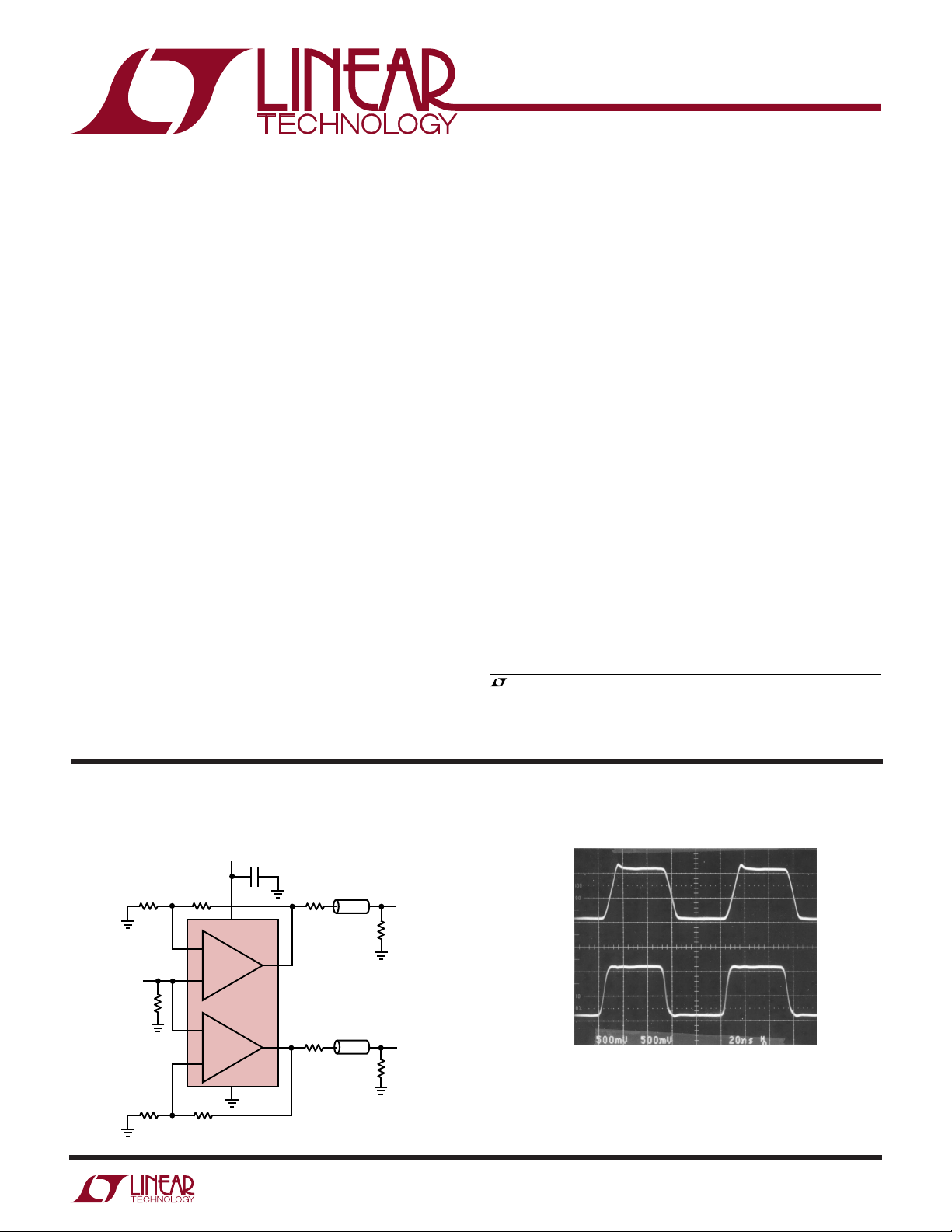
TYPICAL APPLICATIO
Baseband Video Splitter/Cable Driver
3.3V
499Ω 499Ω
2
V
3
IN
75Ω
5
6
499Ω 499Ω
1µF
8
LT6206
–
+
+
–
1
7
4
75Ω
75Ω
F
3dB
≤ 25mA
I
S
U
≈ 50MHz
75Ω
75Ω
620567 TA01a
Output Step Response
V
V
OUT1
V
OUT2
OUT
V
0V
IN
0V
V
= 3.3V
S
= 0.1V TO 1.1V
V
IN
f = 10MHz
20ns/DIV
620567 TA01b
620567f
1
Page 2
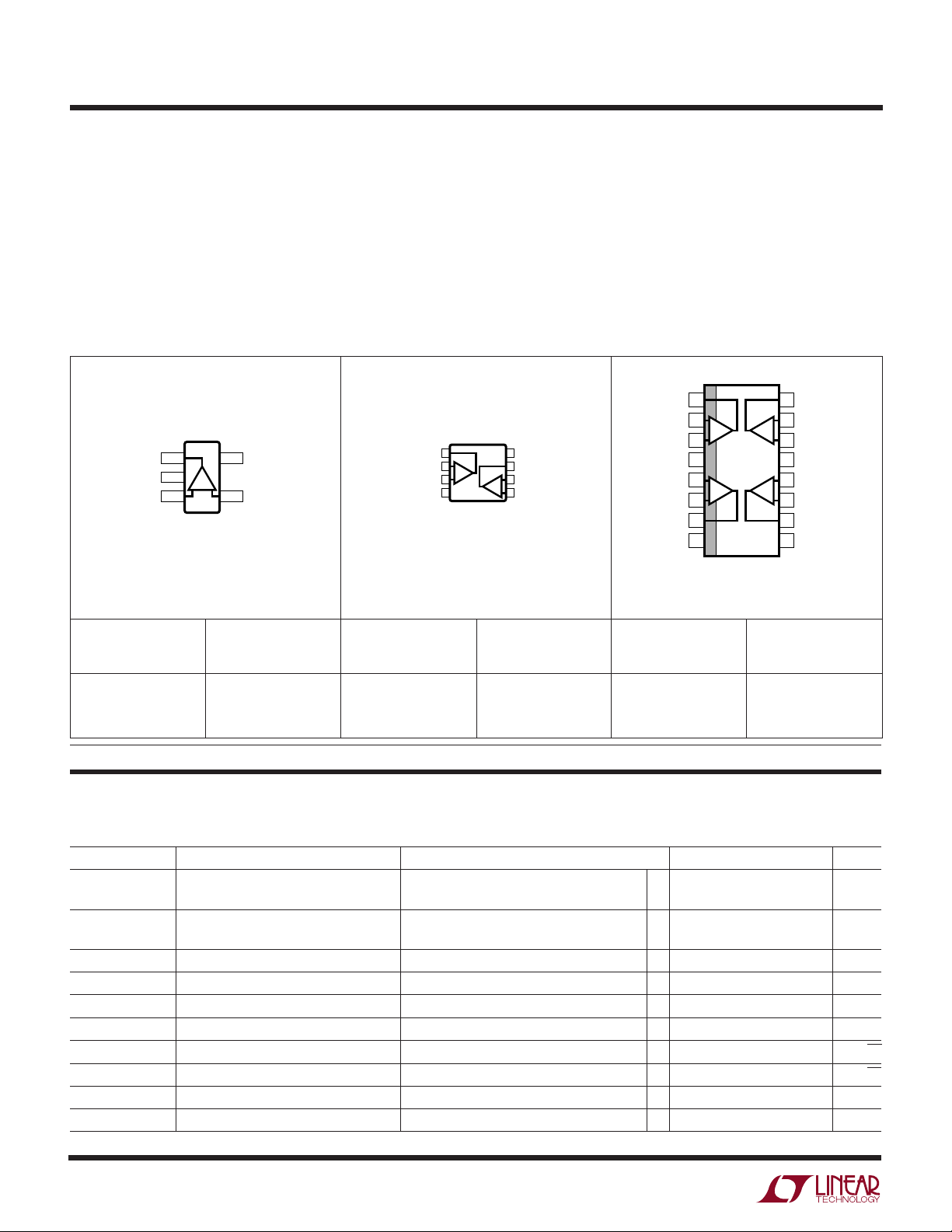
LT6205/LT6206/LT6207
TOP VIEW
GN PACKAGE
16-LEAD NARROW PLASTIC SSOP
1
2
3
4
5
6
7
8
16
15
14
13
12
11
10
9
OUT A
–IN A
+IN A
V
+
+IN B
–IN B
OUT B
NC
OUT D
–IN D
+IN D
V
–
+IN C
–IN C
OUT C
NC
C
–
+
D
+
–
B
–
+
A
+
–
WW
W
U
ABSOLUTE AXI U RATI GS
(Note 1)
Total Supply Voltage (V+ to V–)............................ 12.6V
Input Current ...................................................... ±10mA
Input Voltage Range (Note 2) ...................................±V
Output Short-Circuit Duration (Note 3)............ Indefinite
Pin Current While Exceeding Supplies (Note 9) .. ±25mA
UUW
PACKAGE/ORDER I FOR ATIO
TOP VIEW
OUT 1
–
V
2
+IN 3
5-LEAD PLASTIC SOT-23
T
JMAX
–
+
S5 PACKAGE
= 150°C, θJA = 250°C/W
5 V
4 –IN
+
OUT A
1
–IN A
2
+IN A
3
–
V
4
MS8 PACKAGE
8-LEAD PLASTIC MSOP
T
= 150°C, θJA = 250°C/W
JMAX
Operating Temperature Range .................–40°C to 85°C
Specified Temperature Range (Note 4)....–40°C to 85°C
Storage Temperature Range ..................–65°C to 150°C
S
Maximum Junction Temperature .......................... 150°C
Lead Temperature (Soldering, 10 sec).................. 300°C
TOP VIEW
–
+
+
8
V
7
OUT B
–
6
–IN B
+
5
+IN B
ORDER PART
NUMBER
LT6205CS5
LT6205IS5
*The temperature grades are identified by a label on the shipping container. Consult LTC Marketing for parts specified with wider operating temperature ranges.
ELECTRICAL CHARACTERISTICS
range, otherwise specifications are at TA = 25°C. VS = 3V, 0V; VS = 5V, 0V; VCM = V
SYMBOL PARAMETER CONDITIONS MIN TYP MAX UNITS
V
OS
I
B
I
OS
e
n
i
n
2
T
= 150°C, θJA = 135°C/W
JMAX
S5 PART
MARKING*
LTAEM
ORDER PART
NUMBER
LT6206CMS8
LT6206IMS8
MS8 PART
MARKING
LTH3
LTH4
ORDER PART
NUMBER
LT6207CGN
LT6207IGN
GN PART
MARKING
6207
6207I
The ● denotes specifications which apply over the specified temperature
= 1V, unless otherwise noted.
OUT
Input Offset Voltage 1 3.5 mV
● 5mV
Input Offset Voltage Match 13 mV
(Channel-to-Channel) (Note 5)
Input Offset Voltage Drift (Note 6) ● 715µV/°C
Input Bias Current ● 10 30 µA
Input Offset Current ● 0.6 3 µA
Input Noise Voltage 0.1Hz to 10Hz 2 µV
Input Noise Voltage Density f = 10kHz 9 nV/√Hz
Input Noise Current Density f = 10kHz 4 pA/√Hz
Input Resistance VCM = 0V to V
Input Capacitance 2pF
+
– 2V 1 MΩ
● 4mV
P-P
620567f
Page 3
LT6205/LT6206/LT6207
ELECTRICAL CHARACTERISTICS
range, otherwise specifications are at TA = 25°C. VS = 3V, 0V; VS = 5V, 0V; VCM = V
The ● denotes specifications which apply over the specified temperature
= 1V, unless otherwise noted.
OUT
SYMBOL PARAMETER CONDITIONS MIN TYP MAX UNITS
CMRR Common Mode Rejection Ratio VCM = 0 to V
Input Voltage Range ● 0V
+
– 2V ● 78 90 dB
+
– 2 V
PSRR Power Supply Rejection Ratio VS = 3V to 12V ● 67 75 dB
V
= V
OUT
= 0.5V
CM
Minimum Supply Voltage VCM = 0.5V ● 2.7 V
A
VOL
V
OL
V
OH
I
SC
Large-Signal Voltage Gain VS = 5V, VO = 0.5V to 4.5V, RL = 1k ● 30 100 V/mV
= 5V, VO = 1V to 3V, RL = 150Ω ● 5 20 V/mV
V
S
= 3V, VO = 0.5V to 2.5V, RL = 1k ● 20 60 V/mV
V
S
Output Voltage Swing Low (Note 7) No Load, Input Overdrive = 30mV ● 10 25 mV
= 5mA ● 75 150 mV
I
SINK
V
S
V
S
= 5V, I
= 3V, I
= 25mA ● 300 500 mV
SINK
= 15mA ● 200 350 mV
SINK
Output Voltage Swing High (Note 7) No Load, Input Overdrive = 30mV ● 60 100 mV
= 5mA ● 140 250 mV
I
SOURCE
V
S
V
S
= 5V, I
= 3V, I
= 25mA ● 650 1200 mV
SOURCE
= 15mA ● 300 500 mV
SOURCE
Short-Circuit Current VS = 5V, Output Shorted to GND 35 60 mA
● 25 mA
VS = 3V, Output Shorted to GND 30 50 mA
● 20 mA
I
S
Supply Current per Amplifier 3.75 5 mA
● 5.75 mA
GBW Gain Bandwidth Product f = 2MHz ● 65 100 MHz
SR Slew Rate VS = 5V, AV = 2, RF = RG = 1k 450 V/µs
= 1V to 4V, Measured from 1.5V to 3.5V
V
O
Channel Separation f = 10MHz 90 dB
FPBW Full Power Bandwidth V
t
S
Settling time to 3% VS = 5V, ∆V
OUT
= 2V
(Note 8) 71 MHz
P-P
= 2V, AV = –1, RL = 150Ω 15 ns
OUT
Settling time to 1% 25 ns
Differential Gain VS = 5V, AV = 2, RL = 150Ω, Output Black Level =1V 0.05 %
Differential Phase V
= 5V, AV = 2, RL = 150Ω, Output Black Level =1V 0.08 Deg
S
The ● denotes specifications which apply over the specified temperature range, otherwise specifications are at TA = 25°C. VS = ±5V;
VCM = V
SYMBOL PARAMETER CONDITIONS MIN TYP MAX UNITS
V
OS
I
B
I
OS
= 0V, unless otherwise noted.
OUT
Input Offset Voltage 1.3 4.5 mV
● 6mV
Input Offset Voltage Match 13 mV
(Channel-to-Channel) (Note 5)
● 4mV
Input Offset Voltage Drift (Note 6) ● 10 18 µV/°C
Input Bias Current ● 18 30 µA
Input Offset Current ● 0.6 3 µA
Input Noise Voltage 0.1Hz to 10Hz 2 µV
P-P
620567f
3
Page 4
LT6205/LT6206/LT6207
ELECTRICAL CHARACTERISTICS
range, otherwise specifications are at TA = 25°C. VS = ±5V; VCM = V
SYMBOL PARAMETER CONDITIONS MIN TYP MAX UNITS
e
n
i
n
CMRR Common Mode Rejection Ratio VCM = –5V to 3V ● 78 90 dB
PSRR Power Supply Rejection Ratio VS = ±2V to ±6V ● 67 75 dB
A
VOL
I
SC
I
S
GBW Gain Bandwidth Product f = 2MHz ● 65 100 MHz
SR Slew Rate AV = –1, RL = 1k 350 600 V/µs
FPBW Full Power Bandwidth V
t
S
Note 1: Absolute Maximum ratings are those values beyond which the life
of a device may be impaired.
Note 2: The inputs are protected by back-to-back diodes. If the differential
input voltage exceeds 1.4V, the input current should be limited to less than
10mA.
Note 3: A heat sink may be required to keep the junction temperature
below absolute maximum. This depends on the power supply voltage and
how many amplifiers are shorted.
Note 4: The LT6205C/LT6206C/LT6207C are guaranteed to meet specified
performance from 0°C to 70°C and are designed, characterized and
expected to meet specified performance from –40°C to 85°C but are not
tested or QA sampled at these temperatures. The LT6205I/LT6206I/
LT6207I are guaranteed to meet specified performance from
–40°C to 85°C.
Input Noise Voltage Density f = 10kHz 9 nV/√Hz
Input Noise Current Density f = 10kHz 4 pA/√Hz
Input Resistance VCM = –5V to 3V 1 MΩ
Input Capacitance 2pF
Input Voltage Range ● –5 3 V
Large-Signal Voltage Gain VO = –4V to 4V, RL = 1k ● 50 133 V/mV
VO = –3V to 3V, RL = 150Ω ● 7.5 20 V/mV
Output Voltage Swing No Load, Input Overdrive = 30mV ● ±4.88 ±4.92 V
I
OUT
I
OUT
Short-Circuit Current Short to Ground ±40 ±60 mA
Supply Current per Amplifier 4 5.6 mA
V
Channel Separation f = 10MHz 90 dB
Settling Time to 3% ∆V
Settling Time to 1% 25 ns
Differential Gain AV = 2, RL = 150Ω, Output Black Level = 1V 0.05 %
Differential Phase A
The ● denotes specifications which apply over the specified temperature
= 0V, unless otherwise noted.
OUT
= ±5mA ● ±4.75 ±4.85 V
= ±25mA ● ±3.8 ±4.35 V
● ±30 mA
● 6.5 mA
= –4V to 4V, Measured from –3V to 3V
O
= 8V
OUT
OUT
= 2, RL = 150Ω, Output Black Level = 1V 0.08 Deg
V
(Note 8) 14 24 MHz
P-P
= 2V, AV = –1, RL = 150Ω 15 ns
Note 5: Matching parameters are the difference between the two amplifiers
A and D and between B and C of the LT6207; between the two amplifiers
of the LT6206.
Note 6: This parameter is not 100% tested.
Note 7: Output voltage swings are measured between the output and
power supply rails.
Note 8: Full power bandwidth is calculated from the slew rate
measurement: FPBW = SR/2πV
Note 9: There are reverse biased ESD diodes on all inputs and outputs.
If these pins are forced beyond either supply, unlimited current will flow
through these diodes. If the current is transient in nature and limited to
less than 25mA, no damage to the device will occur.
PEAK
.
4
620567f
Page 5
UW
TEMPERATURE (°C)
–50 –25 0 25 50 75 100 125
INPUT BIAS CURRENT (µA)
620567 G06
–4
–6
–5
–7
–8
–9
–10
–11
–12
VS = 5V, 0V
V
CM
= 1V
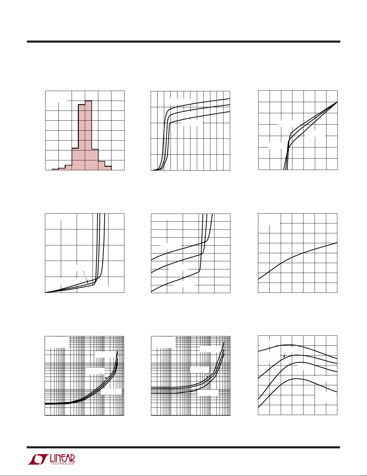
TYPICAL PERFOR A CE CHARACTERISTICS
Supply Current per Amplifier vs
VOS Distribution
40
VS = 5V, 0V
= 1V
V
CM
35
30
25
20
15
PERCENT OF UNITS (%)
10
5
0
–3–2–10123
INPUT OFFSET VOLTAGE (mV)
620567 G01
Supply Voltage Minimum Supply Voltage
5
4
3
2
1
SUPPLY CURRENT PER AMPLIFIER (mA)
0
0123456789101112
TA = 125°C
TA = 25°C
TA = –55°C
TOTAL SUPPLY VOLTAGE (V)
LT6205/LT6206/LT6207
100
0
–100
TA = –55°C
TA =125°C
TA = 25°C
TOTAL SUPPLY VOLTAGE (V)
620567 G03
620567 G02
–200
–300
–400
–500
CHANGE IN INPUT OFFSET VOLTAGE (µV)
–600
1.5 2.0 2.5 3.0 3.5 4.0 4.5 5.0
Change in Offset Voltage vs Input
Common Mode Voltage
1000
VS = 5V, 0V
800
600
400
TA = 25°C
200
OFFSET VOLTAGE CHANGE (µV)
0
TA =125°C
012345
INPUT COMMON MODE VOLTAGE (V)
Output Saturation Voltage vs
Load Current (Output Low)
10
VS = 5V, 0V
= 30mV
V
OD
1
0.1
OUTPUT SATURATION VOLTAGE (V)
0.01
0.01 1 10 100
0.1
LOAD CURRENT (mA)
TA = –55°C
TA = 25°C
TA = 125°C
TA = –55°C
620567 G04
620567 G07
Input Bias Current vs Input
Common Mode Voltage
–2
VS = 5V, 0V
–3
–4
–5
–6
TA = 125°C
–7
–8
–9
INPUT BIAS CURRENT (µA)
–10
–11
–12
012345
TA = 25°C
TA = –55°C
INPUT COMMON MODE VOLTAGE (V)
620567 G05
Output Saturation Voltage vs
Load Current (Output High)
10
VS = 5V, 0V
= 30mV
V
OD
1
0.1
OUTPUT SATURATION VOLTAGE (V)
0.01
0.01 1 10 100
0.1
LOAD CURRENT (mA)
TA = 125°C
TA = 25°C
TA = –55°C
620567 G08
Input Bias Current vs
Temperature
Short-Circuit Current vs
Temperature
75
SINKING
70
VS = 5V, 0V
65
V
CM
60
55
50
45
40
OUTPUT SHORT-CIRCUIT CURRENT (mA)
35
–50 –25 0 25 50 75 100 125
SOURCING
= 1V
TEMPERATURE (°C)
SINKING
SOURCING
VS = 3V, 0V
V
CM
= 1V
620567 G09
620567f
5
Page 6

LT6205/LT6206/LT6207
UW
TYPICAL PERFOR A CE CHARACTERISTICS
Short-Circuit Current vs
Temperature
90
VS = ±5V
80
70
60
50
40
OUTPUT SHORT-CIRCUIT CURRENT (mA)
3O
–50 –25 0 25 50 75 100 125
SINKING
SOURCING
TEMPERATURE (°C)
620567 G10
Open-Loop Gain Open-Loop Gain
500
400
300
200
100
0
–100
–200
INPUT VOLTAGE (µV)
–300
–400
–500
0 1.0 2.0 3.0 4.00.5 1.5 2.5 3.5 4.5 5.0
RL = 1k
RL = 150Ω
OUTPUT VOLTAGE (V)
VS = 5V, 0V
V
CM
T
A
= 1V
= 25°C
620567 G11
500
400
300
200
100
0
–100
–200
INPUT VOLTAGE (µV)
–300
–400
–500
–5 –3 –1 1 3–4 –2 0 2 4 5
OUTPUT VOLTAGE (V)
RL = 150Ω
VS = ±5V
= 25°C
T
A
RL = 1k
620567 G12
Warm Up Drift vs Time (LT6206)
120
100
80
60
40
20
CHANGE IN OFFSET VOLTAGE (µV)
0
0 2040608010 30 50 70 90 100
VS = ±5V
VS = 5V, 0V
TIME AFTER POWER-UP (s)
0.1Hz to 10Hz Noise Voltage
VS = 5V, 0V
= 1V
V
CM
= 25°C
T
A
NOISE VOLTAGE (1µV/DIV)
TIME (2 SEC/DIV)
TA = 25°C
620567 G13
620567 G16
Input Noise Voltage Density vs
Frequency
30
VS = 5V, 0V
= 1V
V
CM
= 25°C
T
25
A
20
15
10
5
INPUT NOISE VOLTAGE DENSITY (nV/√Hz)
0
100 1k 10k 100k
FREQUENCY (Hz)
Gain and Phase vs Frequency
70
60
50
40
30
20
GAIN (dB)
10
0
TA = 25°C
= 1k
R
–10
L
= 5pF
C
L
–20
100k 10M 100M 500M
GAIN
1M
FREQUENCY (Hz)
PHASE
VS = 3V, 0V
VS = ±5V
VS = 3V, 0V
VS = ±5V
620567 G17
620567 G14
140
120
100
80
PHASE (DEG)
60
40
20
0
-20
-40
Input Noise Current Density vs
Frequency
16
VS = 5V, 0V
= 1V
V
CM
14
= 25°C
T
A
12
10
8
6
4
2
INPUT NOISE CURRENT DENSITY (pA/√Hz)
0
100 1k 10k 100k
FREQUENCY (Hz)
Gain Bandwidth and Phase
Margin vs Supply Voltage
TA = 25°C
= RG = 1k
R
F
= 5pF
C
L
110
105
GAIN BANDWIDTH (MHz)
100
95
GAIN BANDWIDTH
024681012
TOTAL SUPPLY VOLTAGE (V)
PHASE MARGIN
620567 G18
620567 G15
50
45
PHASE MARGIN (DEG)
40
35
6
620567f
Page 7

UW
GAIN (AV)
2345
SLEW RATE (V/µs)
620567 G21
750
650
600
700
550
500
400
450
RISING
VS = ±5V
V
O
= –4V to 4V
R
L
= 1k
T
A
= 25°C
FALLING
TYPICAL PERFOR A CE CHARACTERISTICS
Gain Bandwidth and Phase
Margin vs Temperature
620567 G19
55
50
45
PHASE MARGIN (DEG)
40
35
RL = 1k
= 5pF
C
L
VS = 3V, 0V
120
110
GAIN BANDWIDTH (MHz)
VS = 3V, 0V
100
90
80
–50 –25 0 25 50 75 125100
VS = ±5V
PHASE MARGIN
VS = ±5V
GAIN BANDWIDTH
TEMPERATURE (°C)
Closed-Loop Gain vs Frequency Output Impedance vs Frequency
15
TA = 25°C
12
= 5pF
C
L
= +1
A
V
9
6
3
0
GAIN (dB)
–3
–6
–9
–12
–15
100k 10M 100M 500M
1M
FREQUENCY (Hz)
VS = ±5V
V
VS = 3V
= 1V
V
CM
CM
= 0V
OUTPUT IMPEDANCE (Ω)
620567 G22
Slew Rate vs Temperature Slew Rate vs Closed-Loop Gain
750
700
RISING VS = ±5V
650
FALLING VS = ±5V
600
550
RISING VS = 5V, 0V
500
SLEW RATE (V/µs)
450
FALLING VS = 5V, 0V
400
350
–50 –25 0 25 50 75 125100
1000
VS = 5V, 0V
= 25°C
T
A
100
AV = 2
10
1
0.1
100k
TEMPERATURE (°C)
AV = 10
10M 100M1M 500M
FREQUENCY (Hz)
AV = 1
AV = –1
R
R
LT6205/LT6206/LT6207
= RF = 1k
G
= 1k
L
620567 G20
Power Supply Rejection Ratio vs
Frequency
620567 G23
90
80
70
60
50
40
30
20
10
POWER SUPPLY REJECTION RATIO (dB)
+PSRR
0
10k 1M 10M 100M
100k
–PSRR
FREQUENCY (Hz)
VS = 5V, 0V
= 25°C
T
A
620567 G24
Common Mode Rejection Ratio
vs Frequency
100
90
80
70
60
50
40
30
20
10
COMMON MODE REJECTION RATIO (dB)
0
10k 1M 10M 1G
100k
FREQUENCY (Hz)
VS = ±5V
= 25°C
T
A
100M
620567 G25
Channel Separation vs Frequency
120
VS = ±5V
LT6206 CH A-B
110
LT6207 CH A-D, CH B-C
= 25°C
T
A
100
90
80
70
VOLTAGE GAIN (dB)
60
50
40
1M
10M 100M
FREQUENCY (Hz)
620567 G26
Series Output Resistor vs
Capacitive Load
40
VS = 5V, 0V
= 1
A
V
35
= 25°C
T
A
30
25
20
15
OVERSHOOT (%)
10
5
0
10
RS = 20Ω, RL = ∞
RL = RS = 50Ω
CAPACITIVE LOAD (pF)
RS = 10Ω, RL = ∞
100 1000
620567 G27
620567f
7
Page 8

LT6205/LT6206/LT6207
FREQUENCY (MHz)
0.01 0.1 1 10
DISTORTION (dB)
–30
–40
–50
–60
–70
–80
–90
–100
620567 G31
AV = +1
V
O
= 2V
P–P
VS = 5V, 0V
RL = 1k, 2ND
RL = 1k, 3RD
RL = 150Ω, 3RD
RL = 150Ω, 2ND
FREQUENCY (MHz)
0.01 0.1 1 10
DISTORTION (dB)
–30
–40
–50
–60
–70
–80
–90
–100
620567 G34
AV = +2
V
O
= 2V
P–P
VS = ±5V
RL = 1k, 3RD
RL = 150Ω, 3RD
RL = 150Ω, 2ND
RL = 1k, 2ND
UW
TYPICAL PERFOR A CE CHARACTERISTICS
Series Output Resistor vs
Capacitive Load
40
VS = 5V, 0V
= 2
A
V
35
= 25°C
T
A
30
25
20
15
OVERSHOOT (%)
10
5
0
10
RS = 20Ω, RL = ∞
RL = RS = 50Ω
CAPACITIVE LOAD (pF)
RS = 10Ω, RL = ∞
100 1000
620567 G28
Maximum Undistorted Output
Signal vs Frequency
10
9
)
8
P–P
7
6
5
4
3
2
VS = ±5V
OUTPUT VOLTAGE SWING (V
= 25°C
T
1
A
, HD3 < –30dBc
HD
2
0
0.1 1 10 100
FREQUENCY (MHz)
Distortion vs Frequency Distortion vs Frequency
–30
AV = +2
= 2V
V
O
–40
VS = 5V, 0V
–50
–60
–70
DISTORTION (dB)
–80
P–P
RL = 1k, 2ND
RL = 150Ω, 2ND
RL = 150Ω, 3RD
–30
AV = +1
= 2V
V
O
–40
VS = ±5V
–50
–60
–70
DISTORTION (dB)
–80
P–P
RL = 150Ω, 2ND
Distortion vs Frequency
AV = –1
AV = 2
620567 G30
Distortion vs Frequency
RL = 150Ω, 3RD
–90
–100
0.01 0.1 1 10
8
FREQUENCY (MHz)
RL = 1k, 3RD
620567 G32
Large Signal Response
VS = 5V, 0V
500mV/DIV
0V
VS = 5V, 0V 50ns/DIV
= 1
A
V
R
= 150Ω 620567 G35
L
–90
RL = 1k, 2ND
–100
0.01 0.1 1 10
FREQUENCY (MHz)
RL = 1k, 3RD
Small Signal Response
VS = 5V, 0V
2.5V
50mV/DIV
VS = 5V, 0V 50ns/DIV
= 1
A
V
R
= 150Ω 620567 G36
L
620567 G33
620567f
Page 9

LT6205/LT6206/LT6207
UW
TYPICAL PERFOR A CE CHARACTERISTICS
Large Signal Response VS = ±5V Small Signal Response VS = ±5V Output-Overdrive Recovery
(1V/DIV)
IN
V
0V
1V/DIV
VS = ±5V 50ns/DIV
= 1
A
V
R
= 150Ω 620567 G37
L
0V
50mV/DIV
VS = ±5V 50ns/DIV
= 1
A
V
R
= 150Ω 620567 G38
L
0V
0V
(2V/DIV)
OUT
V
VS = 5V, 0V 100ns/DIV
= 2
A
V
WUUU
APPLICATIO S I FOR ATIO
620567 G39
+IN
–IN
DESD1
DESD2
DESD3
DESD4
+
V
I1 I2 I3
+
V
R
IN
150Ω
D1
–
V
+
V
R
150Ω
–
V
D2
IN
Q2
Q1
D3
D4
Q5
Q3
R1
Q6
Q4
Q7
Q8
R2
Q9 Q10
Q11
R4 R5
I4
R3
COMPLEMENTARY
DRIVE
GENERATOR
Q12
Q13
C
M
Q14
DESD5
DESD6
+
V
OUT
–
V
–
V
620567 F01
Figure 1. Simplified Schematic
620567f
9
Page 10

LT6205/LT6206/LT6207
WUUU
APPLICATIO S I FOR ATIO
Amplifier Characteristics
Figure 1 shows a simplified schematic of the LT6205/
LT6206/LT6207. The input stage consists of transistors
Q1 to Q8 and resistor R1. This topology allows for high
slew rates at low supply voltages. The input common
mode range extends from ground to typically 1.75V from
VCC, and is limited by 2 VBEs plus a saturation voltage of
a current source. There are back-to-back series diodes, D1
to D4, across the + and – inputs of each amplifier to limit
the differential voltage to ±1.4V. RIN limits the current
through these diodes if the input differential voltage exceeds ±1.4V. The input stage drives the degeneration
resistors of PNP and NPN current mirrors, Q9 to Q12,
which convert the differential signals into a single-ended
output. The complementary drive generator supplies current to the output transistors that swing from rail-to-rail.
The current generated through R1, divided by the capacitor CM, determines the slew rate. Note that this current,
and hence the slew rate, are proportional to the magnitude
of the input step. The input step equals the output step
divided by the closed loop gain. The highest slew rates are
therefore obtained in the lowest gain configurations. The
Typical Performance Characteristic Curve of Slew Rate vs
Closed Loop Gain shows the details.
ESD
The LT6205/LT6206/LT6207 have reverse-biased ESD
protection diodes on all inputs and outputs as shown in
Figure 1. If these pins are forced beyond either supply
unlimited current will flow through these diodes. If the
current is transient, and limited to 25mA or less, no
damage to the device will occur.
Layout and Passive Components
With a gain bandwidth product of 100MHz and a slew rate
of 450V/µs the LT6205/LT6206/LT6207 require special
attention to board layout and supply bypassing. Use a
ground plane, short lead lengths and RF-quality low ESR
supply bypass capacitors. The positive supply pin should
be bypassed with a small capacitor (typically 0.01µF to
0.1µF) within 0.25 inches of the pin. When driving heavy
loads, an additional 4.7µ F electrolytic capacitor should be
used. When using split supplies, the same is true for the
negative supply pin. For optimum performance all feedback components and bypass capacitors should be contained in a 0.5 inch by 0.5 inch area. This helps ensure
minimal stray capacitances.
The parallel combination of the feedback resistor and gain
setting resistor on the inverting input can combine with
the input capacitance to form a pole which can degrade
stability. In general, use feedback resistors of 1k or less.
Capacitive Load
The LT6205/LT6206/LT6207 are optimized for wide bandwidth video applications. They can drive a capacitive load
of 20pF in a unity-gain configuration. When driving a
larger capacitive load, a resistor of 10Ω to 50Ω should be
connected between the output and the capacitive load to
avoid ringing or oscillation. The feedback should still be
taken from the output pin so that the resistor will isolate
the capacitive load and ensure stability. The Typical Performance Curves show the output overshoot when driving
a capacitive load with different series resistors.
Video Signal Characteristics
Composite video is the most commonly used signal in
broadcast-grade products and includes Luma (or luminance, the intensity information), Chroma (the colorimetry information) and Sync (vertical and horizontal raster
timing) elements combined into a single signal, NTSC and
PAL being the common formats. Component video for
entertainment systems include separate signal(s) for the
Luma and Chroma (i.e. Y/C or YPbPr) with Sync generally
applied to the Luma channel (Y signal). In some instances,
native RGB signals (separate intensity information for
each primary color: red, green, blue) will have Sync
included as well. All the signal types that include Sync are
electrically similar from a voltage-swing standpoint, though
various timing and bandwidth relationships exist depending on the applicable standard.
The typical video waveforms that include Sync (including
full composite) are specified to have nominal 1V
tude. The lower 0.3V is reserved for “sync tips” that carry
timing information, and by being at a lower potential than
all the other information, represents blacker-than-black
intensity, thereby causing scan retrace activity to be
P-P
ampli-
620567f
10
Page 11

WUUU
APPLICATIO S I FOR ATIO
LT6205/LT6206/LT6207
invisible on a CRT. The “black” level of the waveform is at
(or “setup” very slightly above) the upper limit of the sync
information. Waveform content above the black-level is
intensity information, with peak brightness represented at
the maximum signal level. In the case of composite video,
the modulated color subcarrier is superimposed on the
waveform, but the dynamics remain inside the 1V
(a notable exception is the chroma ramp used for differential-gain and differential-phase measurements, which can
reach 1.15V
DC-Coupled Video Amplifier Considerations
Typically video amplifiers drive cables that are series
terminated (“back-terminated”) at the source and loadterminated at the destination with resistances equal to the
cable characteristic impedance, Z0 (usually 75Ω). This
configuration forms a 2:1 resistor divider in the cabling
that must be accounted for in the driver amplifier by
delivering 2V
150Ω). Driving the cable can require more than 13mA
while the output is approaching the saturation-limits of the
amplifier output. The absolute minimum supply is: V
2 + VOH +VOL. For example, the LT6206 dual operating on
3.3V as shown on the front page of this datasheet, with
exceptionally low VOH ≤ 0.5V and VOL ≤ 0.35V, provides a
design margin of 0.45V. The design margin must be large
enough to include supply variations and DC bias accuracy
for the DC-coupled video input.
Handling AC-Coupled Video Signals
AC-coupled video inputs are intrinsically more difficult to
handle than those with DC-coupling because the average
signal voltage of the video waveform is effected by the
picture content, meaning that the black-level at the amplifier “wanders” with scene brightness. The wander is
measured as 0.56V for a 1V
from black-field to white-field and vice-versa, so an additional 1.12V allowance must be made in the amplifier
supply (assuming gain of 2, so V
For example, an LT6205 operating on 5V has a conserva-
).
P-P
output into an effective 2 • Z0 load (e.g.
P-P
NTSC waveform changing
P-P
= 3.12 + VOH +VOL).
MIN
P-P
limit
MIN
=
tive design margin of 1.03V. The amplifier output (for gain
of 2) must swing +1.47V to –1.65V around the DCoperating point, so the biasing circuitry needs to be
designed accordingly for optimal fidelity.
Clamped AC-Input Cable Driver
A popular method of further minimizing supply requirements with AC-coupling is to employ a simple clamping
scheme as shown in Figure 2. In this circuit, the LT6205
operates from 3.3V by having the sync-tips control the
charge on the coupling capacitor C1, thereby reducing the
black-level input wander to ≈ 0.07V. The only minor
drawback to this circuit is the slight sync-tip compression
(≈ 0.025V at input) due to the diode conduction current,
though the picture content remains full fidelity. This circuit
has nearly the design margin of its DC-coupled counterpart, at 0.31V (for this circuit, V
clamp-diode anode bias is selected to set the sync-tip
output voltage at or slightly above VOL.
YPbPr to RGB Component-Video Converter
The back-page application uses the LT6207 quad to implement a minimum amplifier count topology to transcode
consumer component-video into RGB. In this circuit,
signals only pass through one active stage from any input
to any output, with passive additions being performed by
the cable back-termination resistors. The compromise in
using passive output addition is that the amplifier outputs
must be twice as large as that of a conventional cable
driver. The Y-channel section also has the demanding
requirement that it single-handedly drives all three outputs to full brightness during times of white content, so a
helper current source is used to assure unclipped video
when operating from ±5V supplies. This circuit maps
sync-on-Y to sync on all the RGB channels, and for best
results should have input black-levels at 0V nominal to
prevent clipping.
= 2.14 + VOH +VOL). The
MIN
620567f
11
Page 12

LT6205/LT6206/LT6207
U
TYPICAL APPLICATIO
3.3V
COMPOSITE
VIDEO IN 1V
P–P
C1
4.7µF
LT6205
0.1µF
5
1
2
10k
1k 1k
BAT54
C2
4.7µF
2.4k
4
3
470Ω
–
+
Figure 2. Clamped AC-Input Video Cable Driver
75Ω
I
≤ 19mA
S
VIDEO OUT
75Ω
620567 TA02
12
620567f
Page 13

PACKAGE DESCRIPTIO
LT6205/LT6206/LT6207
U
S5 Package
5-Lead Plastic TSOT-23
(Reference LTC DWG # 05-08-1635)
0.62
MAX
3.85 MAX
0.20 BSC
DATUM ‘A’
NOTE:
1. DIMENSIONS ARE IN MILLIMETERS
2. DRAWING NOT TO SCALE
3. DIMENSIONS ARE INCLUSIVE OF PLATING
4. DIMENSIONS ARE EXCLUSIVE OF MOLD FLASH AND METAL BURR
5. MOLD FLASH SHALL NOT EXCEED 0.254mm
6. JEDEC PACKAGE REFERENCE IS MO-193
2.62 REF
RECOMMENDED SOLDER PAD LAYOUT
PER IPC CALCULATOR
0.30 – 0.50 REF
0.95
REF
1.22 REF
1.4 MIN
0.09 – 0.20
(NOTE 3)
2.80 BSC
1.50 – 1.75
(NOTE 4)
0.80 – 0.90
1.00 MAX
PIN ONE
0.95 BSC
2.90 BSC
(NOTE 4)
1.90 BSC
0.30 – 0.45 TYP
5 PLCS (NOTE 3)
0.01 – 0.10
S5 TSOT-23 0302
620567f
13
Page 14

LT6205/LT6206/LT6207
U
PACKAGE DESCRIPTIO
MS8 Package
8-Lead Plastic MSOP
(Reference LTC DWG # 05-08-1660)
0.889
± 0.127
(.035 ± .005)
5.23
(.206)
MIN
0.42 ± 0.038
(.0165 ± .0015)
TYP
RECOMMENDED SOLDER PAD LAYOUT
0.254
(.010)
GAUGE PLANE
0.18
(.007)
NOTE:
1. DIMENSIONS IN MILLIMETER/(INCH)
2. DRAWING NOT TO SCALE
3. DIMENSION DOES NOT INCLUDE MOLD FLASH, PROTRUSIONS OR GATE BURRS.
MOLD FLASH, PROTRUSIONS OR GATE BURRS SHALL NOT EXCEED 0.152mm (.006") PER SIDE
4. DIMENSION DOES NOT INCLUDE INTERLEAD FLASH OR PROTRUSIONS.
INTERLEAD FLASH OR PROTRUSIONS SHALL NOT EXCEED 0.152mm (.006") PER SIDE
5. LEAD COPLANARITY (BOTTOM OF LEADS AFTER FORMING) SHALL BE 0.102mm (.004") MAX
DETAIL “A”
(.126 – .136)
(.0256)
0° – 6° TYP
DETAIL “A”
3.20 – 3.45
0.65
BSC
0.53 ± 0.152
(.021 ± .006)
SEATING
PLANE
3.00 ± 0.102
(.118 ± .004)
(NOTE 3)
4.90 ± 0.152
(.193 ± .006)
(.043)
0.22 – 0.38
(.009 – .015)
TYP
1.10
MAX
8
12
0.65
(.0256)
BSC
7
6
3
5
4
0.52
(.0205)
REF
3.00 ± 0.102
(.118 ± .004)
(NOTE 4)
0.86
(.034)
REF
0.127 ± 0.076
(.005 ± .003)
MSOP (MS8) 0603
14
620567f
Page 15

PACKAGE DESCRIPTIO
LT6205/LT6206/LT6207
U
GN Package
16-Lead Plastic SSOP (Narrow .150 Inch)
(Reference LTC DWG # 05-08-1641)
.045 ±.005
.254 MIN
RECOMMENDED SOLDER PAD LAYOUT
.007 – .0098
(0.178 – 0.249)
.016 – .050
NOTE:
1. CONTROLLING DIMENSION: INCHES
2. DIMENSIONS ARE IN
3. DRAWING NOT TO SCALE
*DIMENSION DOES NOT INCLUDE MOLD FLASH. MOLD FLASH
SHALL NOT EXCEED 0.006" (0.152mm) PER SIDE
**DIMENSION DOES NOT INCLUDE INTERLEAD FLASH. INTERLEAD
FLASH SHALL NOT EXCEED 0.010" (0.254mm) PER SIDE
(0.406 – 1.270)
INCHES
(MILLIMETERS)
.150 – .165
.0250 TYP.0165 ±.0015
.015 ± .004
(0.38 ± 0.10)
0° – 8° TYP
× 45°
.229 – .244
(5.817 – 6.198)
.053 – .068
(1.351 – 1.727)
.008 – .012
(0.203 – 0.305)
16
15
12
.189 – .196*
(4.801 – 4.978)
12 11 10
14
13
5
4
3
9
678
.004 – .0098
(0.102 – 0.249)
.0250
(0.635)
BSC
.009
(0.229)
REF
.150 – .157**
(3.810 – 3.988)
GN16 (SSOP) 0502
Information furnished by Linear Technology Corporation is believed to be accurate and reliable.
However, no responsibility is assumed for its use. Linear Technology Corporation makes no representation that the interconnection of its circuits as described herein will not infringe on existing patent rights.
620567f
15
Page 16

LT6205/LT6206/LT6207
U
TYPICAL APPLICATIO
YPBPR to RGB Converter
CMPD6001S
4.7k
Y
75Ω
P
B
95.3Ω
P
R
133Ω
174Ω
36Ω
FMMT3906
499Ω165Ω
499Ω365Ω
F
3dB
≤ 60mA
I
S
BLACK LEVELS ≈ 0V
1
2
3
5
6
7
≈ 40MHz
–
+
+
–
5V
LT6207
–5V
1µF
4
13
1µF
16
15
–
14
+
12
+
11
–
10
499Ω
107Ω
80.6Ω
499Ω
R = Y + 1.4 • P
B = Y + 1.8 • P
G = Y – 0.34 • PB – 0.71 • P
150Ω
150Ω
150Ω
150Ω
150Ω
150Ω
R
B
R
R
75Ω
B
75Ω
G
75Ω
620567 TA03
RELATED PARTS
PART NUMBER DESCRIPTION COMMENTS
LT1253/LT1254 Low Cost Dual and Quad Video Amplifiers –3dB Bandwidth = 90MHz, Current Feedback
LT1395/LT1396/LT1397 Single Dual Quad 400MHz Current Feedback Amplifiers 0.1dB Flatness to 100MHz, 80mA Output Drive
LT1675 RGB Multiplexer with Current Feedback Amplifiers –3dB Bandwidth = 250MHz, 100MHz Pixel Switching
LT1809/LT1810 Single/Dual, 180MHz, Rail-to-Rail Input and Output Amplifiers 350V/µs Slew Rate, Shutdown, Low Distortion –90dBc at 5MHz
LT6550/LT6551 3.3V Triple and Quad Video Amplifiers Internal Gain of 2, 110MHz –3dB Bandwidth, Input Common
Modes to Ground
LT6552 3.3V Single Supply Video Difference Amplifier Differential or Single-Ended Gain Block, 600V/µs Slew Rate,
Input Common Modes to Ground
620567f
LT/TP 1003 1K • PRINTED IN USA
16
Linear Technology Corporation
1630 McCarthy Blvd., Milpitas, CA 95035-7417
(408) 432-1900 ● FAX: (408) 434-0507 ● www.linear.com
LINEAR TE CHNO LOG Y CORPORATION 2003
 Loading...