

查询LT6200供应商
FEATURES
■
Low Noise Voltage: 0.95nV/√Hz (100kHz)
■
Gain Bandwidth Product:
LT6200/LT6201 165MHz AV = 1
LT6200-5 800MHz AV ≥ 5
LT6200-10 1.6GHz AV ≥ 10
■
Low Distortion: –80dB at 1MHz, RL = 100Ω
■
Dual LT6201 in Tiny DFN Package
■
Input Common Mode Range Includes Both Rails
■
Output Swings Rail-to-Rail
■
Low Offset Voltage: 1mV Max
■
Wide Supply Range: 2.5V to 12.6V
■
Output Current: 60mA Min
■
SOT-23 and SO-8 Packages
■
Operating Temperature Range –40°C to 85°C
■
Power Shutdown, Thermal Shutdown
U
APPLICATIO S
■
Transimpedance Amplifiers
■
Low Noise Signal Processing
■
Active Filters
■
Rail-to-Rail Buffer Amplifiers
■
Driving A/D Converters
LT6200/LT6200-5
LT6200-10/LT6201
165MHz, Rail-to-Rail Input
and Output, 0.95nV/√Hz
Low Noise, Op Amp Family
U
DESCRIPTIO
The LT®6200/LT6201 are single and dual ultralow noise,
rail-to-rail input and output unity gain stable op amps that
feature 0.95nV/√Hz noise voltage. These amplifiers combine very low noise with a 165MHz gain bandwidth,
50V/µs slew rate and are optimized for low voltage signal
conditioning systems. A shutdown pin reduces supply
current during standby conditions and thermal shutdown
protects the part from overload conditions.
The LT6200-5/LT6200-10 are single amplifiers optimized
for higher gain applications resulting in higher gain bandwidth and slew rate. The LT6200 family maintains its
performance for supplies from 2.5V to 12.6V and are
specified at 3V, 5V and ±5V.
For compact layouts the LT6200/LT6200-5/LT6200-10 are
available in the 6-lead ThinSOTTM and the 8-pin SO package. The dual LT6201 is available in an 8-pin SO package
with standard pinouts as well as a tiny, dual fine pitch
leadless package (DFN). These amplifiers can be used as
plug-in replacements for many high speed op amps to
improve input/output range and noise performance.
, LTC and LT are registered trademarks of Linear Technology Corporation.
ThinSOT is a trademark of Linear Technology Corporation.
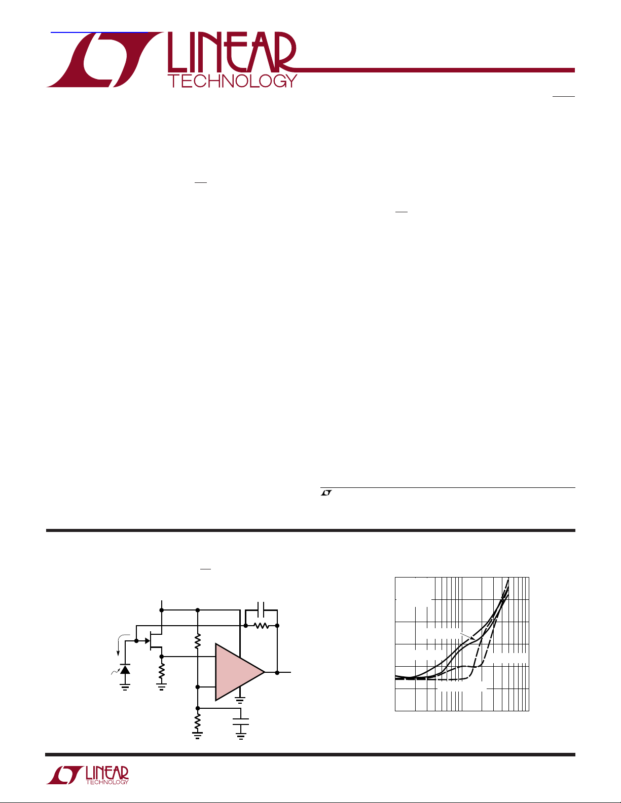
TYPICAL APPLICATIO
Single Supply, 1.5nV/√Hz, Photodiode Amplifier
5V
I
PD
PHOTO
DIODE
PHILIPS
BF862
1k
10k
10k
U
–
+
LT6200
C
R
0.1µF
Distortion vs Frequency
–50
AV = 1
= 2V
V
O
F
F
V
≈ 2V
OUT
+I
• R
PD
F
6200 TA01
–60
–70
–80
–90
DISTORTION (dBc)
–100
–110
100k
P-P
VS = ±2.5V
HD2, RL = 1k
HD2, RL = 100Ω
HD3, RL = 1k
HD3, RL = 100Ω
1M 10M
FREQUENCY (Hz)
6200 G35
62001fa
1

LT6200/LT6200-5
LT6200-10/LT6201
WW
W
ABSOLUTE AXI U RATI GS
U
(Note 1)
Total Supply Voltage (V+ to V–) ............................ 12.6V
Total Supply Voltage (V+ to V–) (LT6201DD) ............. 7V
Input Current (Note 2) ........................................ ±40mA
Output Short-Circuit Duration (Note 3)............ Indefinite
Pin Current While Exceeding Supplies
(Note 12) ............................................................ ±30mA
Operating Temperature Range (Note 4) ...–40°C to 85°C
UUW
PACKAGE/ORDER I FOR ATIO
ORDER PART
NUMBER
LT6200CS6
LT6200IS6
TOP VIEW
OUT 1
–
V
2
+IN 3
S6 PACKAGE
6-LEAD PLASTIC SOT-23
T
= 150°C, θJA = 160°C/W (Note 10)
JMAX
+
6 V
5 SHDN
4 –IN
LT6200CS6-5
LT6200IS6-5
LT6200CS6-10
LT6200IS6-10
S6 PART
MARKING*
LTJZ
LTACB
LTACC
Specified Temperature Range (Note 5)....–40°C to 85°C
Junction Temperature........................................... 150°C
Junction Temperature (DD Package) ................... 125°C
Storage Temperature Range ..................–65°C to 150°C
Storage Temperature Range
(DD Package) ...................................... – 65°C to 125°C
Lead Temperature (Soldering, 10 sec).................. 300°C
ORDER PART
NUMBER
LT6200CS8
LT6200IS8
SHDN
–IN
+IN
TOP VIEW
1
2
–
+
3
–
4
V
NC
8
+
V
7
OUT
6
NC
5
LT6200CS8-5
LT6200IS8-5
LT6200CS8-10
LT6200IS8-10
S8 PART
S8 PACKAGE
8-LEAD PLASTIC SO
T
= 150°C, θJA = 100°C/W
JMAX
MARKING
6200
6200I
62005
6200I5
620010
200I10
TOP VIEW
+
V
1OUT A
–IN A
2
+IN A
8-LEAD (3mm × 3mm) PLASTIC DFN
T
UNDERSIDE METAL CONNECTED TO V
*The temperature grade is identified by a label on the shipping container.
A
3
–
V
4
DD PACKAGE
= 125°C, θJA = 160°C/W (NOTE 3)
JMAX
8
OUT B
7
–IN B
6
B
+IN B
5
–
ORDER PART
NUMBER
LT6201CDD
DD PART
MARKING*
LADG
Consult LTC Marketing for parts specified with wider operating temperature ranges.
2
OUT A
–IN A
+IN A
–
V
T
JMAX
TOP VIEW
1
2
–
+
3
4
S8 PACKAGE
8-LEAD PLASTIC SO
= 150°C, θJA = 100°C/W
–
+
ORDER PART
NUMBER
+
V
8
OUT B
7
–IN B
6
+IN B
5
LT6201CS8
LT6201IS8
S8 PART
MARKING
6201
6201I
62001fa
LT6200/LT6200-5
LT6200-10/LT6201
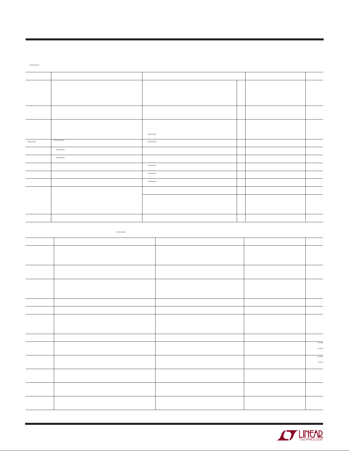
ELECTRICAL CHARACTERISTICS
V
= OPEN, unless otherwise noted.
SHDN
TA = 25°C, VS = 5V, 0V; VS = 3V, 0V; VCM = V
= half supply,
OUT
SYMBOL PARAMETER CONDITIONS MIN TYP MAX UNITS
V
OS
I
B
∆I
B
I
OS
e
n
i
n
Input Offset Voltage VS = 5V, V
VS = 3V, V
VS = 5V, V
= 3V, V
V
S
Input Offset Voltage Match VCM = Half Supply 0.2 1.1 mV
(Channel-to-Channel) (Note 11) V
Input Bias Current V
IB Shift V
IB Match (Channel-to-Channel) (Note 11) V
Input Offset Current V
= V– to V
CM
= Half Supply –40 –10 µA
CM
V
= V
CM
= V
V
CM
= V– to V
CM
= V– to V
CM
= Half Supply 0.1 4 µA
CM
= V
V
CM
= V
V
CM
Input Noise Voltage 0.1Hz to 10Hz 600 nV
=Half Supply 0.1 1 mV
CM
= Half Supply 0.9 2.5 mV
+
–
+
–
CM
= V+ to V
CM
= V+ to V
CM
+
+
+
–
–
0.6 2 mV
1.8 4 mV
0.5 2.2 mV
818 µA
–50 –23 µA
31 68 µA
0.3 5 µA
0.02 4 µA
0.4 5 µA
P-P
Input Noise Voltage Density f = 100kHz, VS = 5V 1.1 nV/√Hz
f = 10kHz, V
= 5V 1.5 2.4 nV/√Hz
S
Input Noise Current Density, Balanced Source f = 10kHz, VS = 5V 2.2 pA/√Hz
Unbalanced Source f = 10kHz, VS = 5V 3.5 pA/√Hz
Input Resistance Common Mode 0.57 MΩ
Differential Mode 2.1 kΩ
C
IN
Input Capacitance Common Mode 3.1 pF
Differential Mode 4.2 pF
A
VOL
Large-Signal Gain VS = 5V, VO = 0.5V to 4.5V, RL = 1k to VS/2 70 120 V/mV
VS = 5V, VO = 1V to 4V, RL = 100Ω to VS/2 11 18 V/mV
V
= 3V, VO = 0.5V to 2.5V, RL = 1k to VS/2 17 70 V/mV
S
CMRR Common Mode Rejection Ratio VS = 5V, V
V
= 5V, V
S
VS = 3V, V
= V– to V
CM
= 1.5V to 3.5V 85 112 dB
CM
= V– to V
CM
+
+
65 90 dB
60 85 dB
CMRR Match (Channel-to-Channel) (Note 11) VS = 5V, VCM = 1.5V to 3.5V 80 105 dB
PSRR Power Supply Rejection Ratio VS = 2.5V to 10V, LT6201DD VS = 2.5V to 7V 60 68 dB
PSRR Match (Channel-to-Channel) (Note 11) VS = 2.5V to 10V, LT6201DD VS = 2.5V to 7V 65 100 dB
Minimum Supply Voltage (Note 6) 2.5 V
V
OL
V
OH
I
SC
I
S
Output Voltage Swing LOW (Note 7) No Load 9 50 mV
I
= 5mA 50 100 mV
SINK
V
= 5V, I
S
VS = 3V, I
= 20mA 150 290 mV
SINK
= 20mA 160 300 mV
SINK
Output Voltage Swing HIGH (Note 7) No Load 55 110 mV
I
= 5mA 95 190 mV
SOURCE
V
= 5V, I
S
VS = 3V, I
= 20mA 220 400 mV
SOURCE
= 20mA 240 450 mV
SOURCE
Short-Circuit Current VS = 5V ±60 ±90 mA
V
= 3V ±50 ±80 mA
S
Supply Current per Amplifier VS = 5V 16.5 20 mA
VS = 3V 15 18 mA
I
SHDN
V
L
V
H
Disabled Supply Current per Amplifier V
SHDN Pin Current V
V
Pin Input Voltage LOW 0.3 V
SHDN
V
Pin Input Voltage HIGH V+ – 0.5 V
SHDN
= 0.3V 1.3 1.8 mA
SHDN
= 0.3V 200 280 µA
SHDN
62001fa
3
LT6200/LT6200-5
LT6200-10/LT6201
ELECTRICAL CHARACTERISTICS
V
= OPEN, unless otherwise noted.
SHDN
TA = 25°C, VS = 5V, 0V; VS = 3V, 0V; VCM = V
= half supply,
OUT
SYMBOL PARAMETER CONDITIONS MIN TYP MAX UNITS
Shutdown Output Leakage Current V
t
ON
t
OFF
Turn-On Time V
Turn-Off Time V
= 0.3V 0.1 75 µA
SHDN
= 0.3V to 4.5V, RL = 100Ω, VS = 5V 130 ns
SHDN
= 4.5V to 0.3V, RL = 100Ω, VS = 5V 180 ns
SHDN
GBW Gain Bandwidth Product Frequency = 1MHz, VS = 5V 145 MHz
LT6200-5 750 MHz
LT6200-10 1450 MHz
SR Slew Rate VS = 5V, AV = –1, RL = 1k, VO = 4V 31 44 V/µs
VS = 5V, AV = –10, RL = 1k, VO = 4V
LT6200-5 210 V/µs
LT6200-10 340 V/µs
FPBW Full Power Bandwidth (Note 9) VS = 5V, V
t
S
Settling Time (LT6200, LT6201) 0.1%, VS = 5V, V
OUT
= 3V
(LT6200) 3.28 4.66 MHz
P-P
= 2V, AV = –1, RL = 1k 165 ns
STEP
The ● denotes the specifications which apply over 0°C < TA < 70°C temperature range. VS = 5V, 0V; VS = 3V, 0V;
V
= V
CM
= half supply, V
OUT
SYMBOL PARAMETER CONDITIONS MIN TYP MAX UNITS
V
OS
Input Offset Voltage VS = 5V, V
Input Offset Voltage Match VCM = Half Supply ● 0.2 1.8 mV
(Channel-to-Channel) (Note 11) V
VOS TC Input Offset Voltage Drift (Note 8) V
I
B
Input Bias Current V
IB Match (Channel-to-Channel) (Note 11) VCM = V– to V
∆I
B
I
OS
A
VOL
IB Shift V
Input Offset Current V
Large-Signal Gain VS = 5V, VO = 0.5V to 4.5V,RL = 1k to VS/2 ● 46 80 V/mV
CMRR Common Mode Rejection Ratio VS = 5V, V
CMRR Match (Channel-to-Channel) (Note 11) VS = 5V, VCM = 1.5V to 3.5V ● 80 105 dB
PSRR Power Supply Rejection Ratio VS = 3V to 10V, LT6201DD VS = 3V to 7V ● 60 65 dB
PSRR Match (Channel-to-Channel) (Note 11) VS = 3V to 10V, LT6201DD VS = 3V to 7V ● 60 100 dB
Minimum Supply Voltage (Note 6) ● 3V
V
OL
V
OH
Output Voltage Swing LOW (Note 7) No Load ● 12 60 mV
Output Voltage Swing HIGH (Note 7) No Load ● 65 120 mV
= OPEN, unless otherwise noted.
SHDN
V
VS = 5V, V
V
V
V
V
V
V
VS = 3V, VO = 0.5V to 2.5V,RL = 1k to VS/2 ● 13 22 V/mV
VS = 5V, V
VS = 3V, V
I
VS = 5V, I
VS = 3V, I
I
V
VS = 3V, I
= Half Supply ● 0.2 1.2 mV
CM
= 3V, V
S
= 3V, V
S
= V– to V
CM
= Half Supply ● 2.5 8 µV/°C
CM
= Half Supply ● –40 –10 µA
CM
= V
CM
= V
CM
= V– to V
CM
= Half Supply ● 0.1 4 µA
CM
= V
CM
= V
CM
= 5V, VO = 1.5V to 3.5V,RL = 100Ω to VS/2 ● 7.5 13 V/mV
S
SINK
SOURCE
= 5V, I
S
= Half Supply ● 1.0 2.7 mV
CM
= V+ to V
CM
= V+ to V
CM
+
+
–
+
+
+
–
= V– to V
CM
= 1.5V to 3.5V ● 80 105 dB
CM
= V– to V
CM
–
–
+
+
● 0.3 3 mV
● 1.5 4 mV
● 0.4 2.8 mV
● 818 µA
● –50 –23 µA
● 0.5 6 µA
● 31 68 µA
● 0.02 4 µA
● 0.4 5 µA
● 64 88 dB
● 60 83 dB
= 5mA ● 55 110 mV
= 20mA ● 170 310 mV
SINK
= 20mA ● 170 310 mV
SINK
= 5mA ● 115 210 mV
= 20mA ● 260 440 mV
SOURCE
= 20mA ● 270 490 mV
SOURCE
62001fa
4
LT6200/LT6200-5
LT6200-10/LT6201
ELECTRICAL CHARACTERISTICS
temperature range. VS = 5V, 0V; VS = 3V, 0V; V
CM
= V
The ● denotes the specifications which apply over 0°C < TA < 70°C
= half supply, V
OUT
= OPEN, unless otherwise noted.
SHDN
SYMBOL PARAMETER CONDITIONS MIN TYP MAX UNITS
I
SC
Short-Circuit Current VS = 5V ● ±60 ±90 mA
VS = 3V ● ±45 ±75 mA
I
S
Supply Current per Amplifier VS = 5V ● 20 23 mA
VS = 3V ● 19 22 mA
I
SHDN
V
L
V
H
t
ON
t
OFF
Disabled Supply Current per Amplifier V
SHDN Pin Current V
V
Pin Input Voltage LOW ● 0.3 V
SHDN
V
Pin Input Voltage HIGH ● V+ – 0.5 V
SHDN
Shutdown Output Leakage Current V
Turn-On Time V
Turn-Off Time V
= 0.3V ● 1.35 1.8 mA
SHDN
= 0.3V ● 215 295 µA
SHDN
= 0.3V ● 0.1 75 µA
SHDN
= 0.3V to 4.5V, RL = 100Ω, VS = 5V ● 130 ns
SHDN
= 4.5V to 0.3V, RL = 100Ω, VS = 5V ● 180 ns
SHDN
SR Slew Rate VS = 5V, AV = –1, RL = 1k, VO = 4V ● 29 42 V/µs
AV = –10, RL = 1k, VO = 4V
LT6200-5 ● 190 V/µs
LT6200-10
FPBW Full Power Bandwidth (Note 9) VS = 5V, V
OUT
= 3V
(LT6200) ● 3.07 4.45 MHz
P-P
● 310 V/µs
The ● denotes the specifications which apply over –40°C < TA < 85°C temperature range. Excludes the LT6201 in the DD package
(Note 3). VS = 5V, 0V; VS = 3V, 0V; V
SYMBOL PARAMETER CONDITIONS MIN TYP MAX UNITS
V
OS
VOS TC Input Offset Voltage Drift (Note 8) V
I
B
∆I
B
I
OS
A
VOL
CMRR Common Mode Rejection Ratio VS = 5V, V
PSRR Power Supply Rejection Ratio VS = 3V to 10V ● 60 68 dB
V
OL
Input Offset Voltage VS = 5V, V
Input Offset Voltage Match VCM = Half Supply ● 0.2 2 mV
(Channel-to-Channel) (Note 11) V
Input Bias Current V
IB Shift V
IB Match (Channel-to-Channel) (Note 11) V
Input Offset Current V
Large-Signal Gain VS = 5V, VO = 0.5V to 4.5V, RL = 1k to VS/2 ● 40 70 V/mV
CMRR Match (Channel-to-Channel) (Note 11) VS = 5V, VCM = 1.5V to 3.5V ● 75 105 dB
PSRR Match (Channel-to-Channel) (Note 11) VS = 3V to 10V ● 60 100 dB
Minimum Supply Voltage (Note 6) ● 3V
Output Voltage Swing LOW (Note 7) No Load ● 18 70 mV
CM
= V
= half supply, V
OUT
= OPEN, unless otherwise noted. (Note 5)
SHDN
= Half Supply ● 0.2 1.5 mV
CM
= 3V, V
V
S
VS = 5V, V
= 3V, V
V
S
= V– to V
CM
CM
CM
V
CM
V
CM
CM
CM
CM
V
CM
V
CM
= 5V, VO = 1.5V to 3.5V, RL = 100Ω to VS/2 ● 7.5 13 V/mV
V
S
= Half Supply ● 1.0 2.8 mV
CM
= V+ to V
CM
= V+ to V
CM
+
–
–
● 0.3 3.5 mV
● 1.5 4.3 mV
● 0.4 3 mV
= Half Supply ● 2.5 8.0 µV/°C
= Half Supply ● –40 –10 µA
+
= V
–
= V
= V– to V
= V– to V
= Half Supply ● 0.1 4 µA
= V
= V
+
+
+
–
● 818 µA
● –50 –23 µA
● 31 68 µA
● 19 µA
● 0.02 4 µA
● 0.4 5 µA
VS = 3V, VO = 0.5V to 2.5V,RL = 1k to VS/2 ● 11 20 V/mV
= V– to V
VS = 5V, V
VS = 3V, V
I
SINK
VS = 5V, I
VS = 3V, I
CM
= 1.5V to 3.5V ● 80 100 dB
CM
= V– to V
CM
= 5mA ● 60 120 mV
SINK
SINK
+
+
● 60 80 dB
● 60 80 dB
= 20mA ● 170 310 mV
= 20mA ● 175 315 mV
62001fa
5
LT6200/LT6200-5
LT6200-10/LT6201
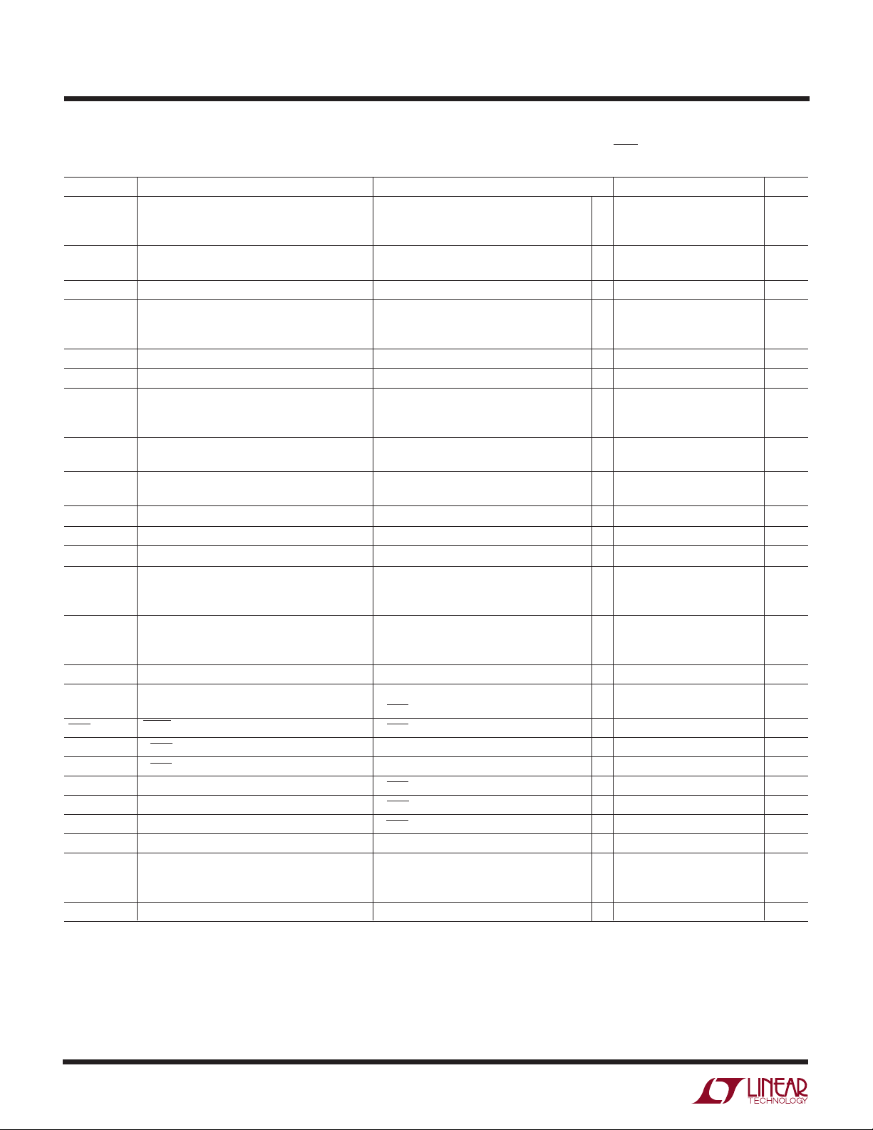
ELECTRICAL CHARACTERISTICS
temperature range. Excludes the LT6201 in the DD package (Note 3). VS = 5V, 0V; VS = 3V, 0V; V
V
= OPEN, unless otherwise noted. (Note 5)
SHDN
The ● denotes the specifications which apply over –40°C < TA < 85°C
= V
CM
= half supply,
OUT
SYMBOL PARAMETER CONDITIONS MIN TYP MAX UNITS
V
OH
I
SC
I
S
I
SHDN
V
L
V
H
t
ON
t
OFF
Output Voltage Swing HIGH (Note 7) No Load ● 65 120 mV
I
= 5mA ● 115 210 mV
SOURCE
VS = 5V, I
= 3V, I
V
S
= 20mA ● 270 450 mV
SOURCE
= 20mA ● 280 500 mV
SOURCE
Short-Circuit Current VS = 5V ● ±50 ±80 mA
= 3V ● ±30 ±60 mA
V
S
Supply Current per Amplifier VS = 5V ● 22 25.3 mA
= 3V ● 20 23 mA
V
Disabled Supply Current per Amplifier V
SHDN Pin Current V
V
Pin Input Voltage LOW ● 0.3 V
SHDN
V
Pin Input Voltage HIGH ● V+ – 0.5 V
SHDN
Shutdown Output Leakage Current V
Turn-On Time V
Turn-Off Time V
S
= 0.3V ● 1.4 1.9 mA
SHDN
= 0.3V ● 220 300 µA
SHDN
= 0.3V ● 0.1 75 µA
SHDN
= 0.3V to 4.5V, RL = 100Ω, VS = 5V ● 130 ns
SHDN
= 4.5V to 0.3V, RL = 100Ω, VS = 5V ● 180 ns
SHDN
SR Slew Rate VS = 5V, AV = –1, RL = 1k, VO = 4V ● 23 33 V/µs
AV = –10, RL = 1k, VO = 4V
LT6200-5 ● 160 V/µs
LT6200-10 ● 260 V/µs
FPBW Full Power Bandwidth (Note 9) VS = 5V, V
OUT
= 3V
(LT6200) ● 2.44 3.5 MHz
P-P
TA = 25°C, VS = ±5V, VCM = V
OUT
= 0V, V
= OPEN, unless otherwise noted. Excludes the LT6201 in the DD package (Note 3).
SHDN
SYMBOL PARAMETER CONDITIONS MIN TYP MAX UNITS
V
OS
I
B
∆I
B
I
OS
e
n
Input Offset Voltage V
Input Offset Voltage Match VCM = 0V 0.2 1.6 mV
(Channel-to-Channel) (Note 11) V
Input Bias Current V
IB Shift V
IB Match (Channel-to-Channel) (Note 11) V
Input Offset Current V
Input Noise Voltage 0.1Hz to 10Hz 600 nV
= Half Supply 1.4 4 mV
CM
+
V
= V
CM
–
V
= V
CM
= V– to V
CM
= Half Supply – 40 –10 µA
CM
V
= V
CM
V
= V
CM
= V– to V
CM
= V– to V
CM
= Half Supply 1.3 7 µA
CM
V
= V
CM
V
= V
CM
+
+
–
+
+
+
–
–50 –23 µA
2.5 6 mV
2.5 6 mV
0.4 3.2 mV
818 µA
31 68 µA
0.2 6 µA
17 µA
312 µA
P-P
Input Noise Voltage Density f = 100kHz 0.95 nV/√Hz
f = 10kHz 1.4 2.3 nV/√Hz
i
n
Input Noise Current Density, Balanced Source f = 10kHz 2.2 pA/√Hz
Unbalanced Source f = 10kHz 3.5 pA/√Hz
Input Resistance Common Mode 0.57 MΩ
Differential Mode 2.1 kΩ
C
IN
Input Capacitance Common Mode 3.1 pF
Differential Mode 4.2 pF
A
VOL
Large-Signal Gain VO = ±4.5V, RL = 1k 115 200 V/mV
V
= ±2V, RL = 100 15 26 V/mV
O
6
62001fa
LT6200/LT6200-5
LT6200-10/LT6201
ELECTRICAL CHARACTERISTICS
TA = 25°C, VS = ±5V, VCM = V
OUT
= 0V, V
= OPEN, unless otherwise
SHDN
noted. Excludes the LT6201 in the DD package (Note 3).
SYMBOL PARAMETER CONDITIONS MIN TYP MAX UNITS
CMRR Common Mode Rejection Ratio VCM = V– to V
V
= –2V to 2V 75 100 dB
CM
CMRR Match (Channel-to-Channel) (Note 11) VCM = –2V to 2V 80 105 dB
PSRR Power Supply Rejection Ratio VS = ±1.25V to ±5V 60 68 dB
PSRR Match (Channel-to-Channel) (Note 6) VS = ±1.25V to ±5V 65 100 dB
V
OL
V
OH
I
SC
I
S
I
SHDN
V
L
V
H
t
ON
t
OFF
GBW Gain Bandwidth Product Frequency = 1MHz 110 165 MHz
SR Slew Rate AV = –1, RL = 1k, VO = 4V 35 50 V/µs
FPBW Full Power Bandwidth (Note 9) V
t
S
Output Voltage Swing LOW (Note 7) No Load 12 50 mV
I
SINK
I
SINK
Output Voltage Swing HIGH (Note 7) No Load 70 130 mV
I
SOURCE
I
SOURCE
Short-Circuit Current ±60 ±90 mA
Supply Current per Amplifier 20 23 mA
Disabled Supply Current per Amplifier V
SHDN Pin Current V
V
Pin Input Voltage LOW 0.3 V
SHDN
V
Pin Input Voltage HIGH V+ – 0.5 V
SHDN
Shutdown Output Leakage Current V
Turn-On Time V
Turn-Off Time V
Settling Time (LT6200, LT6201) 0.1%, V
SHDN
SHDN
SHDN
SHDN
SHDN
LT6200-5 530 800 MHz
LT6200-10 1060 1600 MHz
AV = –10, RL = 1k, VO = 4V
LT6200-5 175 250 V/µs
LT6200-10 315 450 V/µs
OUT
+
= 5mA 55 110 mV
= 20mA 150 290 mV
= 5mA 110 210 mV
= 20mA 225 420 mV
= 0.3V 1.6 2.1 mA
= 0.3V 200 280 µA
= 0.3V 0.1 75 µA
= 0.3V to 4.5V, RL = 100Ω, VS = 5V 130 ns
= 4.5V to 0.3V, RL = 100Ω, VS = 5V 180 ns
= 3V
(LT6200-10) 33 47 MHz
P-P
= 2V, AV = –1, RL = 1k 140 ns
STEP
68 96 dB
62001fa
7
LT6200/LT6200-5
LT6200-10/LT6201
ELECTRICAL CHARACTERISTICS
temperature range. Excludes the LT6201 in the DD package (Note 3). VS = ±5V, V
The ● denotes the specifications which apply over 0°C < TA < 70°C
= V
CM
OUT
= 0V, V
= OPEN, unless
SHDN
otherwise noted.
SYMBOL PARAMETER CONDITIONS MIN TYP MAX UNITS
V
OS
VOS TC Input Offset Voltage Drift (Note 8) V
I
B
∆I
B
I
OS
A
VOL
CMRR Common Mode Rejection Ratio V
PSRR Power Supply Rejection Ratio VS = ±1.5V to ±5V ● 60 65 dB
V
OL
V
OH
I
SC
I
S
I
SHDN
V
L
V
H
t
ON
t
OFF
SR Slew Rate AV = –1, RL = 1k, VO = 4V ● 31 44 V/µs
FPBW Full Power Bandwidth (Note 9) V
Input Offset Voltage V
Input Offset Voltage Match VCM = 0V ● 0.2 1.8 mV
(Channel-to-Channel) (Note 11) V
Input Bias Current V
IB Shift V
IB Match (Channel-to-Channel) (Note 11) V
Input Offset Current V
= Half Supply ● 1.9 4.5 mV
CM
+
V
= V
CM
–
V
= V
CM
= V– to V
CM
= Half Supply ● 8.2 24 µV/°C
CM
= Half Supply ● –40 –10 µA
CM
V
= V
CM
V
= V
CM
= V– to V
CM
= V– to V
CM
= Half Supply ● 1.3 10 µA
CM
V
= V
CM
V
= V
CM
+
+
–
+
+
+
–
● 3.5 7.5 mV
● 3.5 7.5 mV
● 0.4 3.4 mV
● 818 µA
● –50 –23 µA
● 31 68 µA
● 19 µA
● 1.0 10 µA
● 3.5 15 µA
Large-Signal Gain VO = ±4.5V, RL = 1k ● 46 80 V/mV
VO = ±2V, RL = 100 ● 7.5 13.5 V/mV
= V– to V
CM
V
= –2V to 2V ● 75 100 dB
CM
+
● 65 90 dB
CMRR Match (Channel-to-Channel) (Note 11) VCM = –2V to 2V ● 75 105 dB
PSRR Match (Channel-to-Channel) (Note 6) VS = ±1.5V to ±5V ● 60 100 dB
Output Voltage Swing LOW (Note 7) No Load ● 16 70 mV
I
= 5mA ● 60 120 mV
SINK
I
= 20mA ● 170 310 mV
SINK
Output Voltage Swing HIGH (Note 7) No Load ● 85 150 mV
I
= 5mA ● 125 230 mV
SOURCE
I
= 20mA ● 265 480 mV
SOURCE
Short-Circuit Current ● ±60 ±90 mA
Supply Current per Amplifier ● 25 29 mA
Disabled Supply Current per Amplifier V
SHDN Pin Current V
V
Pin Input Voltage LOW ● 0.3 V
SHDN
V
Pin Input Voltage HIGH ● V+ – 0.5 V
SHDN
Shutdown Output Leakage Current V
Turn-On Time V
Turn-Off Time V
= 0.3V ● 1.6 2.1 mA
SHDN
= 0.3V ● 215 295 µA
SHDN
= 0.3V ● 0.1 75 µA
SHDN
= 0.3V to 4.5V, RL = 100Ω, VS = 5V ● 130 ns
SHDN
= 4.5V to 0.3V, RL = 100Ω, VS = 5V ● 180 ns
SHDN
AV = –10, RL = 1k, VO = 4V
LT6200-5 ● 150 215 V/µs
LT6200-10
= 3V
OUT
(LT6200-10) ● 30 43 MHz
P-P
● 290 410 V/µs
8
62001fa

LT6200/LT6200-5
LT6200-10/LT6201
ELECTRICAL CHARACTERISTICS
temperature range. Excludes the LT6201 in the DD package (Note 3). VS = ±5V, V
The ● denotes the specifications which apply over –40°C < TA < 85°C
= V
CM
OUT
= 0V, V
= OPEN, unless
SHDN
otherwise noted. (Note 5)
SYMBOL PARAMETER CONDITIONS MIN TYP MAX UNITS
V
OS
VOS TC Input Offset Voltage Drift (Note 8) V
I
B
∆I
B
I
OS
A
VOL
CMRR Common Mode Rejection Ratio V
PSRR Power Supply Rejection Ratio VS = ±1.5V to ±5V ● 60 65 dB
V
OL
V
OH
I
SC
I
S
I
SHDN
V
L
V
H
t
ON
t
OFF
SR Slew Rate AV = –1, RL = 1k, VO = 4V ● 31 44 V/µs
FPBW Full Power Bandwidth (Note 9) V
Input Offset Voltage V
Input Offset Voltage Match VCM = 0V ● 0.2 2.0 mV
(Channel-to-Channel) (Note 11) VCM = V– to V
Input Bias Current V
IB Shift V
= Half Supply ● 1.9 4.5 mV
CM
+
V
= V
CM
–
V
= V
CM
+
= Half Supply ● 8.2 24 µV/°C
CM
= Half Supply ● –40 –10 µA
CM
+
V
= V
CM
–
V
= V
CM
CM
= V– to V
+
● 3.5 7.5 mV
● 3.5 7.5 mV
● 0.4 3.6 mV
● 818 µA
● –50 –23 µA
● 31 68 µA
IB Match (Channel-to-Channel) (Note 11) ● 412 µA
Input Offset Current V
= Half Supply ● 1.3 10 µA
CM
+
V
= V
CM
–
V
= V
CM
● 1.0 10 µA
● 3.5 15 µA
Large-Signal Gain VO = ±4.5V, RL = 1k ● 46 80 V/mV
V
= ±2V RL = 100 ● 7.5 13.5 V/mV
O
CM
V
CM
+
= V– to V
● 65 90 dB
= –2V to 2V ● 75 100 dB
CMRR Match (Channel-to-Channel) (Note 11) VCM = –2V to 2V ● 75 105 dB
PSRR Match (Channel-to-Channel) (Note 6) VS = ±1.5V to ±5V ● 60 100 dB
Output Voltage Swing LOW (Note 7) No Load ● 16 75 mV
I
= 5mA ● 60 125 mV
SINK
I
= 20mA ● 170 310 mV
SINK
Output Voltage Swing HIGH (Note 7) No Load ● 85 150 mV
I
= 5mA ● 125 230 mV
SOURCE
I
= 20mA ● 265 480 mV
SOURCE
Short-Circuit Current ● ±60 ±90 mA
Supply Current ● 25 29 mA
Disabled Supply Current V
SHDN Pin Current V
V
Pin Input Voltage LOW ● 0.3 V
SHDN
V
Pin Input Voltage HIGH ● V+ – 0.5 V
SHDN
Shutdown Output Leakage Current V
Turn-On Time V
Turn-Off Time V
= 0.3V ● 1.6 2.1 mA
SHDN
= 0.3V ● 215 295 µA
SHDN
= 0.3V ● 0.1 75 µA
SHDN
= 0.3V to 4.5V, RL = 100Ω, VS = 5V ● 130 ns
SHDN
= 4.5V to 0.3V, RL = 100Ω, VS = 5V ● 180 ns
SHDN
AV = –10, RL = 1k, VO = 4V
LT6200-5
● 125 180 V/µs
LT6200-10 ● 260 370 V/µs
= 3V
OUT
(LT6200-10) ● 27 39 MHz
P-P
Note 1: Absolute maximum ratings are those values beyond which the life
of the device may be impaired.
Note 2: Inputs are protected by back-to-back diodes. If the differential
input voltage exceeds 0.7V, the input current must be limited to less than
40mA.
Note 3: A heat sink may be required to keep the junction temperature
below the absolute maximum rating when the output is shorted
indefinitely. The LT6201 in the DD package is limited by power dissipation
≤ 5V, 0V over the commercial temperature range only.
to V
S
Note 4: The LT6200C/LT6200I and LT6201C/LT6201I are guaranteed
functional over the temperature range of –40°C and 85°C (LT6201DD
excluded).
62001fa
9

LT6200/LT6200-5
LT6200-10/LT6201
ELECTRICAL CHARACTERISTICS
Note 5: The LT6200C/LT6201C are guaranteed to meet specified
performance from 0°C to 70°C. The LT6200C/LT6201C are designed,
characterized and expected to meet specified performance from – 40°C to
85°C, but are not tested or QA sampled at these temperatures. The
LT6200I is guaranteed to meet specified performance from –40°C to 85°C.
Note 6: Minimum supply voltage is guaranteed by power supply rejection
ratio test.
Note 7: Output voltage swings are measured between the output and
power supply rails.
Note 8: This parameter is not 100% tested.
Note 9: Full-power bandwidth is calculated from the slew rate:
FPBW = SR/2πV
P
Note 10: Thermal resistance varies depending upon the amount of PC
board metal attached to the V
certain amount of 2oz copper metal trace connecting to the V
described in the thermal resistance tables in the Application Information
section.
Note 11: Matching parameters on the LT6201 are the difference between
the two amplifiers. CMRR and PSRR match are defined as follows: CMRR
and PSRR are measured in µV/V on the identical amplifiers. The difference
is calculated in µV/V. The result is converted to dB.
Note 12: There are reverse biased ESD diodes on all inputs and outputs as
shown in Figure 1. If these pins are forced beyond either supply, unlimited
current will flow through these diodes. If the current is transient in nature
and limited to less than 30mA, no damage to the device will occur.
UW
TYPICAL PERFOR A CE CHARACTERISTICS
VOS Distribution, VCM = V+/2
80
VS = 5V, 0V
SO-8
70
60
50
40
30
NUMBER OF UNITS
20
10
0
–600 –200 200 1000
–1000
INPUT OFFSET VOLTAGE (µV)
600
6200 G01
VOS Distribution, VCM = V
80
VS = 5V, 0V
SO-8
70
60
50
40
30
NUMBER OF UNITS
20
10
0
–1600–1200
–800 –400
INPUT OFFSET VOLTAGE (µV)
0 400
+
800 1200
6200 G02
1600
–
pin of the device. θJA is specified for a
VOS Distribution, VCM = V
80
VS = 5V, 0V
SO-8
70
60
50
40
30
NUMBER OF UNITS
20
10
0
–1600–1200
–800 –400
INPUT OFFSET VOLTAGE (µV)
0 400
–
pin as
–
800 1200
1600
6200 G03
Supply Current vs Supply Voltage
30
25
20
15
10
SUPPLY CURRENT (mA)
5
0
0
24
TOTAL SUPPLY VOLTAGE (V)
TA = 125°C
TA = 25°C
TA = –55°C
81214
610
10
6200 G04
Offset Voltage
vs Input Common Mode Voltage
3.0
2.5
2.0
1.5
1.0
0.5
0
OFFSET VOLTAGE (mV)
–0.5
–1.0
–1.5
0
INPUT COMMON MODE VOLTAGE (V)
TA = 125°C
TA = 25°C
TA = –55°C
13
2
VS = 5V, 0V
TYPICAL PART
4
6200 G05
Input Bias Current
vs Common Mode Voltage
20
VS = 5V, 0V
10
0
–10
–20
INPUT BIAS CURRENT (µA)
–30
–40
5
–1
TA = –55°C
TA = 25°C
TA = 125°C
356
01
COMMON MODE VOLTAGE (V)
24
6200 G06
62001fa

UW
TYPICAL PERFOR A CE CHARACTERISTICS
LT6200/LT6200-5
LT6200-10/LT6201
Input Bias Current
vs Temperature
20
VS = 5V, 0V
15
VCM = 5V
VCM = 0V
25 85
10
TEMPERATURE (°C)
INPUT BIAS CURRENT (µA)
10
5
0
–5
–10
–15
–20
–25
–30
–35 –5
–50
–20
Minimum Supply Voltage
1.0
VCM = VS/2
0.5
0
TA = –55°C
–0.5
–1.0
–1.5
CHANGE IN OFFSET VOTLAGE (mV)
–2.0
1234
TOTAL SUPPLY VOLTAGE (V)
55
40
TA = 125°C
70
6200 G07
TA = 25°C
6200 G10
Output Saturation Voltage
vs Load Current (Output Low)
10
VS = 5V, 0V
1
0.1
0.01
OUTPUT SATURATION VOLTAGE (V)
0.001
0.1
Output Short-Circuit Current
vs Power Supply Voltage Open-Loop Gain
120
SOURCING
100
TA = 25°C
80
60
40
20
0
–20
–40
SINKING
–60
–80
–100
OUTPUT SHORT-CIRCUIT CURRENT (mA)
–120
50.50 1.5 2.5 3.5 4.5
1.5
TA = 125°C
TA = –55°C
TA = 25°C
1 10 100
LOAD CURRENT (mA)
TA = –55°C
TA = 125°C
TA = 25°C
TA = 125°C
2.5
2
POWER SUPPLY VOLTAGE (±V)
TA = –55°C
3.5
3
4
6200 G08
4.5
6200 G11
Output Saturation Voltage
vs Load Current (Output High)
10
VS = 5V, 0V
1
0.1
OUTPUT SATURATION VOLTAGE (V)
0.01
–0.5
–1.0
INPUT VOLTAGE (mV)
–1.5
–2.0
5
–2.5
TA = 125°C
TA = 25°C
0.1
2.5
2.0
1.5
1.0
0.5
0
0
TA = –55°C
1 10 100
LOAD CURRENT (mA)
= 1k
R
L
RL = 100Ω
0.5
1.5 2
1
OUTPUT VOLTAGE (V)
6200 G09
VS = 3V, 0V
= 25°C
T
A
2.5
6200 G12
3
Open-Loop Gain Open-Loop Gain Offset Voltage vs Output Current
2.5
2.0
1.5
1.0
0.5
0
–0.5
–1.0
INPUT VOLTAGE (mV)
–1.5
–2.0
–2.5
1
0
OUTPUT VOLTAGE (V)
= 1k
R
L
RL = 100Ω
2
VS = 5V, 0V
= 25°C
T
A
34
6200 G13
2.5
2.0
1.5
1.0
0.5
0
–0.5
–1.0
INPUT VOLTAGE (mV)
–1.5
–2.0
5
–2.5
RL = 1k
–3–4
–5
–1–2
0
OUTPUT VOLTAGE (V)
VS = ±5V
= 25°C
T
A
RL = 100Ω
12 4
3
6200 G14
5
15
VS = ±5V
10
5
0
–5
OFFSET VOLTAGE (mV)
–10
–15
T
TA = –55°C TA = 25°C
–60 –20 20 60
OUTPUT CURRENT (mA)
= 125°C
A
100–100
6200 G15
62001fa
11

LT6200/LT6200-5
LT6200-10/LT6201
UW
TYPICAL PERFOR A CE CHARACTERISTICS
Warm-Up Drift
vs Time (LT6200S8) Total Noise vs Source Resistance Input Noise Voltage vs Frequency
300
TA = 25°C
250
200
150
100
VS = ±1.5V
50
CHANGE IN OFFSET VOLTAGE (µV)
0
VS = ±2.5V
0
40 80
20 60
TIME AFTER POWER-UP (SEC)
VS = ±5V
100
120
140
160
6200 G16
100
VS = ±5V
= 0V
V
CM
f = 100kHz
UNBALANCED
SOURCE
10
RESISTORS
1
TOTAL NOISE VOLTAGE (nV/√Hz)
0.1
10 1k 10k 100k
100
SOURCE RESISTANCE (Ω)
LT6200
TOTAL NOISE
RESISTOR
NOISE
LT6200 AMPLIFIER
NOISE VOLTAGE
6200 G17
NOISE VOLTAGE (nV/√Hz)
45
40
35
30
25
20
15
10
5
0
10
PNP ACTIVE
V
= 0.5V
CM
100
NPN ACTIVE
= 4.5V
V
CM
BOTH ACTIVE
V
= 2.5V
CM
1k
FREQUENCY (Hz)
VS = 5V, 0V
T
= 25°C
A
10k
6200 G18
100k
Balanced Noise Current
vs Frequency
25
20
PNP ACTIVE
= 0.5V
V
CM
15
10
5
BALANCED NOISE CURRENT (pA/√Hz)
0
10 1k 10k 100k
BOTH ACTIVE
= 2.5V
V
CM
NPN ACTIVE
V
CM
100
FREQUENCY (Hz)
= 4.5V
VS = 5V, 0V
T
A
BALANCED
SOURCE
RESISTANCE
Supply Current
vs SHDN Pin Voltage
22
= 5V, 0V
V
S
20
18
16
14
12
10
8
6
SUPPLY CURRENT (mA)
4
2
0
1234
0
SHDN PIN VOLTAGE (V)
= 25°C
TA = –55°C
6200 G19
TA = 25°C
UNBALANCED NOISE CURRENT (pA/√Hz)
TA = 125°C
Unbalanced Noise Current
vs Frequency
35
30
PNP ACTIVE
25
20
15
10
5
0
10 1k 10k 100k
= 0.5V
V
CM
100
BOTH ACTIVE
= 2.5V
V
CM
NPN ACTIVE
= 4.5V
V
CM
FREQUENCY (Hz)
VS = 5V, 0V
= 25°C
T
A
UNBALANCED
SOURCE
RESISTANCE
SHDN Pin Current
vs SHDN Pin Voltage
50
V
0
–50
–100
–150
–200
SHDN PIN CURRENT (µA)
–250
5
6200 G43
–300
0
0.1Hz to 10Hz Output Noise
Voltage
800
VS = 5V, 0V
= VS/2
V
CM
600
400
200
0
–200
–400
OUTPUT VOLTAGE NOISE (nV)
–600
–800
6200 G20
= 5V, 0V
S
TA = 25°C
T
= –55°C
A
T
= 125°C
A
123 5
SHDN PIN VOLTAGE (V)
4
TIME (5SEC/DIV)
6200 G21
6200 G44
12
62001fa

UW
FREQUENCY (Hz)
40
COMMON MODE REJECTION RATIO (dB)
80
120
20
60
100
10k 1M 10M 100M 1G
6200 G28
0
100k
VS = 5V, 0V
V
CM
= VS/2
TYPICAL PERFOR A CE CHARACTERISTICS
Gain Bandwidth and Phase
Margin vs Temperature Open-Loop Gain vs Frequency
VS = ±5V
VS = 3V, 0V
PHASE MARGIN
180
160
GAIN BANDWIDTH (MHz)
140
120
100
–50
–25
80
70
60
50
40
30
GAIN (dB)
20
10
0
VCM = 0V
= 5pF
C
–10
L
= 1k
R
L
–20
100k 10M 100M 1G
1M
VS = ±5V
VS = 3V, 0V
GAIN BANDWIDTH
0
25 125
50
TEMPERATURE (°C)
PHASE
GAIN
VS = ±1.5V
FREQUENCY (Hz)
75 100
VS = ±5V
VS = ±1.5V
VS = ±5V
6200 G22
6200 G24
70
60
50
PHASE MARGIN (DEG)
40
120
100
80
60
PHASE (DEG)
40
20
0
–20
–40
–60
–80
80
70
60
50
40
30
GAIN (dB)
20
10
–10
–20
180
160
140
GAIN BANDWIDTH (MHz)
120
100
80
LT6200/LT6200-5
LT6200-10/LT6201
LT6200, LT6201
PHASE
VCM = 0.5V
GAIN
VCM = 4.5V
0
VS = 5V, 0V
= 5pF
C
L
= 1k
R
L
100k 10M 100M 1G
1M
FREQUENCY (Hz)
Gain Bandwidth and Phase
Margin vs Supply VoltageOpen-Loop Gain vs Frequency
TA = 25°C
= 1k
R
L
= 5pF
C
L
0
4
2
TOTAL SUPPLY VOLTAGE (V)
VCM = 4.5V
VCM = 0.5V
PHASE MARGIN
GAIN BANDWIDTH
8
6
6200 G23
10
12
6200 G25
120
100
80
60
PHASE (DEG)
40
20
0
–20
–40
–60
–80
80
70
60
PHASE MARGIN (DEG)
50
40
30
14
Slew Rate vs Temperature
140
AV = –1
= RG = 1k
R
F
120
= 1k
R
L
100
80
SLEW RATE (V/µs)
60
40
20
0
–55 –35 –15 5 25 45 65 85 105
VS = ±5V FALLING
VS = ±2.5V FALLING
TEMPERATURE (°C)
VS = ±5V RISING
VS = ±2.5V RISING
6200 G26
125
1000
VS = 5V, 0V
100
= 10
A
V
10
1
OUTPUT IMPEDANCE (Ω)
0.1
0.01
0.1 1 10
AV = 2
AV = 1
FREQUENCY (MHz)
Common Mode Rejection Ratio
vs FrequencyOutput Impedance vs Frequency
100
6200 G27
62001fa
13

LT6200/LT6200-5
LT6200-10/LT6201
UW
TYPICAL PERFOR A CE CHARACTERISTICS
Power Supply Rejection Ratio
vs Frequency Overshoot vs Capacitive Load
80
70
60
50
40
30
20
10
POWER SUPPLY REJECTION RATIO (dB)
0
10k
1k 100k 1M 100M
FREQUENCY (Hz)
NEGATIVE
SUPPLY
VS = 5V, 0V
V
T
A
POSITIVE
SUPPLY
10M
= VS/2
CM
= 25°C
6200 G29
40
VS = 5V, 0V
= 1
A
V
35
30
25
20
15
OVERSHOOT (%)
10
RS = 50Ω
R
5
0
10
RS = 20Ω
= 50Ω
L
100 1000
CAPACITIVE LOAD (pF)
RS = 10Ω
LT6200, LT6201
Overshoot vs Capacitive Load
60
VS = 5V, 0V
A
50
40
30
OVERSHOOT (%)
20
10
0
10
6200 G30
= 2
V
RS = 20Ω
RS = 50Ω
R
CAPACITIVE LOAD (pF)
RS = 10Ω
= 50Ω
L
100 1000
6200 G31
Settling Time vs Output Step
(Noninverting)
200
VS = ±5V
= 1
A
V
= 25°C
T
A
150
100
SETTLING TIME (ns)
50
0
1mV 1mV
10mV 10mV
–4
–3 –2 –1 0
OUTPUT STEP (V)
–
+
V
IN
Distortion vs Frequency, AV = 1
–50
AV = 1
= 2V
V
O
–60
–70
–80
–90
DISTORTION (dBc)
–100
–110
100k
P-P
VS = ±2.5V
HD2, RL = 1k
HD2, RL = 100Ω
HD3, RL = 100Ω
1M 10M
FREQUENCY (Hz)
V
OUT
500Ω
1234
6200 G32
HD3, RL = 1k
6200 G35
Settling Time vs Output Step
(Inverting)
200
VS = ±5V
= –1
A
V
= 25°C
T
A
150
100
SETTLING TIME (ns)
50
10mV 10mV
0
–4
–3 –2 –1 0
500Ω
V
IN
1mV
OUTPUT STEP (V)
–
+
Distortion vs Frequency, AV = 1
–50
AV = 1
= 2V
V
O
–60
–70
–80
–90
DISTORTION (dBc)
–100
–110
100k
P-P
VS = ±5V
HD2, RL = 1k
HD2, RL = 100Ω
HD3, RL = 100Ω
1M 10M
FREQUENCY (Hz)
500Ω
V
OUT
1mV
1234
6200 G33
HD3, RL = 1k
6200 G36
Maximum Undistorted Output
Signal vs Frequency
10
AV = –1
9
)
P-P
8
7
6
5
4
VS = ±5V
OUTPUT VOLTAGE SWING (V
3
= 25°C
T
A
HD2, HD3 < –40dBc
2
10k
AV = 2
100k 1M 10M
FREQUENCY (Hz)
Distortion vs Frequency, AV = 2
–40
AV = 2
= 2V
V
O
–50
–60
–70
–80
DISTORTION (dBc)
–90
–100
–110
100k
P-P
VS = ±2.5V
HD2, RL = 100Ω
HD3, RL = 100Ω
HD2, RL = 1k
1M
FREQUENCY (Hz)
6200 G34
HD3, RL = 1k
10M
6200 G37
14
62001fa

UW
TYPICAL PERFOR A CE CHARACTERISTICS
LT6200/LT6200-5
LT6200-10/LT6201
LT6200, LT6201
Distortion vs Frequency, AV = 2
–40
AV = 2
= 2V
V
O
–50
–60
–70
–80
DISTORTION (dBc)
–90
–100
–110
100k
P-P
VS = ±5V
HD2, RL = 100Ω
HD2, RL = 1k
HD3, RL = 100Ω
1M
FREQUENCY (Hz)
5V Large-Signal Response
5V
1V/DIV
0V
HD3, RL = 1k
6200 G38
10M
Channel Separation vs Frequency
0
TA = 25°C
–10
A
= 1
V
–20
V
= ±5V
S
–30
–40
–50
–60
–70
–80
VOLTAGE GAIN (dB)
–90
–100
–110
–120
0.1
1 10 100
FREQUENCY (MHz)
±5V Large-Signal Response
2V/DIV
0V
6200 G77
V
1V/DIV
V
OUT
2V/DIV
V
= 5V, 0V 200ns/DIV 6200 G39
S
AV = 1
= 1k
R
L
Output Overdrive Recovery
0V
IN
0V
= 5V, 0V 200ns/DIV 6200 G42
V
S
AV = 2
50mV/DIV
V
= ±5V 200ns/DIV 6200 G41
S
AV = 1
R
= 1k
L
5V Small-Signal Response
VS = 5V, 0V 200ns/DIV 6200 G40
AV = 1
= 1k
R
L
62001fa
15

LT6200/LT6200-5
FREQUENCY (Hz)
30
GAIN (dB)
PHASE (DEG)
90
100
20
10
80
50
70
60
40
100k 10M 100M 1G
6200 G50
–10
0
100
120
80
20
60
40
0
1M
VS = ±5V
GAIN
PHASE
VS = ±5V
VS = ±1.5V
VS = ±1.5V
VCM = 0V
C
L
= 5pF
R
L
= 1k
RESISTOR LOAD (Ω)
0
0
GAIN BANDWIDTH (MHz)
100
300
400
500
600 700 800 900
900
G200 G53
200
100 200 300 400 500 1000
600
700
800
VS = ±5V
R
F
= 10k
R
G
= 1k
T
A
= 25°C
LT6200-10/LT6201
UW
TYPICAL PERFOR A CE CHARACTERISTICS
Gain Bandwidth and Phase Margin
vs Temperature
PHASE MARGIN
1000
GAIN BANDWIDTH
900
800
GAIN BANDWIDTH (MHz)
700
600
500
–50
0
–25
TEMPERATURE (°C)
VS = ±5V
VS = 3V, 0V
VS = ±5V
VS = 3V, 0V
25 125
50
75 100
6200 G45
90
80
70
PHASE MARGIN (DEG)
60
50
Slew Rate vs Temperature Overshoot vs Capacitive Load
450
AV = –5
R
= RL = 1k
F
400
R
= 200Ω
G
350
300
250
200
SLEW RATE (V/µs)
150
100
VS = ±5V FALLING
0
–55 –25 0 25 50 75 100
VS = ±5V RISING
VS = ±2.5V FALLING
VS = ±2.5V RISING
TEMPERATURE (°C)
LT6200-5
125
6200 G46
60
VS = 5V, 0V
= 5
A
V
50
40
30
OVERSHOOT (%)
20
10
0
10
RS = 0Ω
RS = 50Ω
100 1000
CAPACITIVE LOAD (pF)
RS = 10Ω
RS = 20Ω
6200 G47
Power Supply Rejection Ratio
vs Frequency
80
POSITIVE
70
60
50
40
30
20
10
POWER SUPPLY REJECTION RATIO (dB)
SUPPLY
NEGATIVE
SUPPLY
0
10k
1k 100k 1M 100M
FREQUENCY (Hz)
Open-Loop Gain vs Frequency
100
90
80
70
60
50
40
GAIN (dB)
30
20
10
0
–10
100k 10M 100M 1G
16
PHASE
GAIN
VS = 5V, 0V
= 5pF
C
L
= 1k
R
L
VCM = 4.5V
1M
FREQUENCY (Hz)
VCM = 0.5V
VCM = 4.5V
VCM = 0.5V
VS = 5V, 0V
= 25°C
T
A
= VS/2
V
CM
10M
6200 G48
6200 G51
Output Impedance vs Frequency Open-Loop Gain vs Frequency
1000
VS = 5V, 0V
100
10
1
OUTPUT IMPEDANCE (Ω)
0.1
0.01
100k 1M 10M
Gain Bandwidth and Phase Margin
vs Supply Voltage Gain Bandwidth vs Resistor Load
120
100
80
60
PHASE (DEG)
40
20
0
–20
–40
–60
–80
–100
TA = 25°C
= 1k
R
L
= 5pF
C
L
1000
GAIN BANDWIDTH (MHz)
800
600
400
0
AV = 50
AV = 5
FREQUENCY (Hz)
PHASE MARGIN
GAIN BANDWIDTH
24 8
TOTAL SUPPLY VOLTAGE (V)
6
6200 G49
10
100M
6200 G52
90
80
PHASE MARGIN (DEG)
70
60
50
12
62001fa

UW
TYPICAL PERFOR A CE CHARACTERISTICS
LT6200/LT6200-5
LT6200-10/LT6201
LT6200-5
Common Mode Rejection Ratio
vs Frequency
120
VS = 5V, 0V
= VS/2
V
CM
100
80
60
40
20
COMMON MODE REJECTION RATIO (dB)
0
10k 1M 10M 100M 1G
100k
FREQUENCY (Hz)
6200 G54
Maximum Undistorted Output
Signal vs Frequency
10
9
)
8
P-P
7
6
5
4
3
2
VS = ±5V
OUTPUT VOLTAGE SWING (V
= 5
A
1
V
= 25°C
T
A
0
10k 1M 10M 100M
100k
FREQUENCY (Hz)
2nd and 3rd Harmonic Distortion
vs Frequency ±5V Large-Signal Response
–40
AV = 5
= 2V
V
O
VS = ±5V
P-P
RL = 100Ω, 3RD
RL = 1k, 2ND
RL = 100Ω, 2ND
5V
2V/DIV 0V
–5V
–50
–60
–70
–80
DISTORTION (dB)
–90
6200 G55
2nd and 3rd Harmonic Distortion
vs Frequency
–40
AV = 5
= 2V
V
O
VS = ±2.5V
10k
P-P
RL = 100Ω, 3RD
RL = 100Ω, 2ND
RL = 1k, 2ND
RL = 1k, 3RD
100k 1M 10M
FREQUENCY (Hz)
–50
–60
–70
–80
DISTORTION (dB)
–90
–100
Output-Overdrive Recovery
V
IN
1V/DIV
0V
V
OUT
2V/DIV
0V
6200 G56
–100
–110
10k
RL = 1k, 3RD
100k 1M 10M
FREQUENCY (Hz)
6200 G57
5V Small-Signal Response
50mV/DIV 0V
V
= 5V, 0V 50ns/DIV 6200 G61
S
AV = 5
= 1k
R
L
= 10.8pF SCOPE PROBE
C
L
= ±5V 50ns/DIV 6200 G58
V
S
AV = 5
R
= 1k
L
= 10.8pF SCOPE PROBE
C
L
10nV
1nV/√Hz/DIV
0nV
100kHz 15MHz/DIV 150MHz
= 5V, 0V 50ns/DIV 6200 G59
V
S
AV = 5
C
= 10.8pF SCOPE PROBE
L
Input Referred High Frequency
Noise Spectrum
NOISE LIMITED BY INSTRUMENT NOISE FLOOR
6200 G60
62001fa
17

LT6200/LT6200-5
FREQUENCY (Hz)
30
GAIN (dB)
PHASE (DEG)
90
100
20
10
80
50
70
60
40
100k 10M 100M 1G
6200 G67
–10
0
100
120
80
20
60
40
0
1M
VS = ±5V
VS = ±5V
GAIN
PHASE
VCM = 0V
C
L
= 5pF
R
L
= 1k
VS = ±1.5V
VS = ±1.5V
RESISTOR LOAD (Ω)
0
0
GAIN BANDWIDTH (MHz)
200
600
800
1000
600 700 800 900
1800
G200 G70
400
100 200 300 400 500 1000
1200
1400
1600
VS = ±5V
R
F
= 10k
R
G
= 1k
T
A
= 25°C
LT6200-10/LT6201
UW
TYPICAL PERFOR A CE CHARACTERISTICS
Gain Bandwidth and Phase Margin
vs Temperature Slew Rate vs Temperature Overshoot vs Capacitive Load
750
AV = –10
700
= RL = 1k
R
F
R
= 100Ω
650
G
600
PHASE MARGIN (DEG)
550
500
450
400
350
SLEW RATE (v/µs)
300
250
200
150
VS = ±5V FALLING
–50
–25
VS = ±5V RISING
VS = ±2.5V FALLING
VS = ±2.5V RISING
25
0
TEMPERATURE (°C)
PHASE MARGIN
2000
GAIN BANDWIDTH
1800
1600
GAIN BANDWIDTH (MHz)
1400
1200
1000
–50
0
–25
TEMPERATURE (°C)
VS = ±5V
VS = 3V, 0V
VS = ±5V
VS = 3V, 0V
25 125
50
75 100
80
70
60
50
6200 G62
50
LT6200-10
75
100
6200 G63
125
60
VS = 5V, 0V
= 10
A
V
50
40
30
OVERSHOOT (%)
20
10
RS = 50Ω
0
10
RS = 20Ω
CAPACITIVE LOAD (pF)
RS = 0Ω
RS = 10Ω
100 1000
6200 G64
Power Supply Rejection Ratio
vs Frequency Output Impedance vs Frequency Open-Loop Gain vs Frequency
80
70
60
50
40
30
20
10
POWER SUPPLY REJECTION RATIO (dB)
0
1k 100k 1M 100M
POSITIVE
SUPPLY
NEGATIVE
SUPPLY
10k
FREQUENCY (Hz)
Open-Loop Gain vs Frequency
100
90
80
70
60
50
40
GAIN (dB)
30
20
10
VS = 5V, 0V
C
0
R
–10
100k 10M 100M 1G
18
PHASE
GAIN
VCM = 4.5V
= 5pF
L
= 1k
L
1M
FREQUENCY (Hz)
VCM = 4.5V
VCM = 0.5V
VCM = 0.5V
VS = 5V, 0V
= 25°C
T
A
= VS/2
V
CM
10M
6200 G65
6200 G68
1000
100
10
1
OUTPUT IMPEDANCE (Ω)
0.1
0.01
100k 1M 10M
120
100
80
60
PHASE (DEG)
40
20
0
–20
–40
–60
–80
–100
1800
1600
GAIN BANDWIDTH (MHz)
1400
1200
1000
VS = 5V, 0V
AV = 100
AV = 10
FREQUENCY (Hz)
100M
6200 G66
Gain Bandwidth and Phase Margin
vs Supply Voltage Gain Bandwidth vs Resistor Load
TA = 25°C
R
= 1k
L
C
= 5pF
L
PHASE MARGIN
GAIN BANDWIDTH
24 8
0
TOTAL SUPPLY VOLTAGE (V)
6
90
80
PHASE MARGIN (DEG)
70
60
50
10
12
6200 G69
62001fa

UW
FREQUENCY (Hz)
10k
–100
DISTORTION (dB)
–60
–50
–40
100k 1M 10M
6200 G73
–70
–80
–90
AV = 10
V
O
= 2V
P-P
VS = ±2.5V
RL = 100Ω, 3RD
RL = 100Ω, 2ND
RL = 1k, 2ND
RL = 1k, 3RD
TYPICAL PERFOR A CE CHARACTERISTICS
LT6200/LT6200-5
LT6200-10/LT6201
LT6200-10
Common Mode Rejection Ratio
vs Frequency
120
VS = 5V, 0V
= VS/2
V
CM
100
80
60
40
20
COMMON MODE REJECTION RATIO (dB)
0
10k 1M 10M 100M 1G
100k
FREQUENCY (Hz)
6200 G71
Maximum Undistorted Output
Signal vs Frequency
10
9
)
8
P-P
7
6
5
4
3
2
VS = ±5V
OUTPUT VOLTAGE SWING (V
= 10
A
1
V
= 25°C
T
A
0
10k 1M 10M 100M
100k
FREQUENCY (Hz)
2nd and 3rd Harmonic Distortion
vs Frequency ±5V Large-Signal Response
–40
AV = 10
= 2V
V
O
VS = ±5V
P-P
RL = 100Ω, 3RD
RL = 1k, 3RD
5V
RL = 100Ω, 2ND
2V/DIV 0V
–5V
–50
–60
–70
–80
DISTORTION (dB)
–90
6200 G72
2nd and 3rd Harmonic Distortion
vs Frequency
Output-Overdrive Recovery
V
IN
1V/DIV
0V
V
OUT
2V/DIV
0V
–100
–110
10k
50mV/DIV 0V
RL = 1k, 2ND
100k 1M 10M
FREQUENCY (Hz)
= ±5V 50ns/DIV 6200 G75
V
S
AV = 10
R
= 1k
L
= 10.8pF SCOPE PROBE
C
L
6200 G74
5V Small-Signal Response
VS = 5V, 0V 50ns/DIV 6200 G78
AV = 10
R
= 1k
L
= 10.8pF SCOPE PROBE
C
L
10nV
1nV/√Hz/DIV
0nV
V
= 5V, 0V 50ns/DIV 6200 G76
S
AV = 10
C
= 10.8pF SCOPE PROBE
L
Input Referred High Frequency
Noise Spectrum
100kHz 15MHz/DIV 150MHz
6200 G77
62001fa
19

LT6200/LT6200-5
LT6200-10/LT6201
U
WUU
APPLICATIO S I FOR ATIO
Amplifier Characteristics
Figure 1 shows a simplified schematic of the LT6200
family, which has two input differential amplifiers in parallel that are biased on simultaneously when the common
mode voltage is at least 1.5V from either rail. This topology
allows the input stage to swing from the positive supply
voltage to the negative supply voltage. As the common
mode voltage swings beyond V
I1 saturates and current in Q1/Q4 is zero. Feedback is
maintained through the Q2/Q3 differential amplifier, but
with an input gm reduction of 1/2. A similar effect occurs
with I2 when the common mode voltage swings within
1.5V of the negative rail. The effect of the gm reduction is
a shift in the VOS as I1 or I2 saturate.
Input bias current normally flows out of the + and – inputs.
The magnitude of this current increases when the input
common mode voltage is within 1.5V of the negative rail,
and only Q1/Q4 are active. The polarity of this current
reverses when the input common mode voltage is within
1.5V of the positive rail and only Q2/Q3 are active.
The second stage is a folded cascode and current mirror
that converts the input stage differential signals to a single
ended output. Capacitor C1 reduces the unity cross
frequency and improves the frequency stability without
degrading the gain bandwidth of the amplifier. The
differential drive generator supplies current to the output
transistors that swing from rail-to-rail.
– 1.5V, current source
CC
The LT6200-5/LT6200-10 are decompensated op amps for
higher gain applications. These amplifiers maintain identical DC specifications with the LT6200, but have a reduced
Miller compensation capacitor CM. This results in a significantly higher slew rate and gain bandwidth product.
Input Protection
There are back-to-back diodes, D1 and D2, across the
+ and – inputs of these amplifiers to limit the differential
input voltage to ±0.7V. The inputs of the LT6200 family do
not have internal resistors in series with the input transistors. This technique is often used to protect the input
devices from overvoltage that causes excessive currents
to flow. The addition of these resistors would significantly
degrade the low noise voltage of these amplifiers. For
instance, a 100Ω resistor in series with each input would
generate 1.8nV/√Hz of noise, and the total amplifier noise
voltage would rise from 0.95nV/√Hz to 2.03nV/√Hz. Once
the input differential voltage exceeds ±0.7V, steady-state
current conducted though the protection diodes should be
limited to ±40mA. This implies 25Ω of protection resistance per volt of continuous overdrive beyond ±0.7V. The
input diodes are rugged enough to handle transient currents due to amplifier slew rate overdrive or momentary
clipping without these resistors.
Figure 2 shows the input and output waveforms of the
LT6200 driven into clipping while connected in a gain of
20
DESD1
+
–
+
V
R1 R2
I
1
+V
–V
DESD2
DESD4DESD3
–V
+V
Q1 Q4
Q2 Q3
D2D1
R3 R4 R5
I
2
Figure 1. Simplified Schematic
Q5
C1
Q8
D3
BIAS
Q6
C
M
+V
Q9
DIFFERENTIAL
DRIVE
GENERATOR
Q7
6203/04 F01
Q11
Q10
DESD7
V
SHDN
DESD8
–V
+V
DESD5
DESD6
–V
–
V
62001fa

LT6200/LT6200-5
LT6200-10/LT6201
U
WUU
APPLICATIO S I FOR ATIO
AV = 1. In this photo, the input signal generator is clipping
at ±35mA, and the output transistors supply this generator current through the protection diodes.
V
CC
2.5V
0V
V
EE
–2.5V
Figure 2. VS = ±2.5V, AV = 1 with Large Overdrive
Power Dissipation
The LT6200 combines high speed with large output current in a small package, so there is a need to ensure that
the die’s junction temperature does not exceed 150°C. The
LT6200 is housed in a 6-lead TSOT-23 package. The
package has the V– supply pin fused to the lead frame to
enhance the thermal conductance when connecting to a
ground plane or a large metal trace. Metal trace and plated
through-holes can be used to spread the heat generated by
the device to the backside of the PC board. For example, on
a 3/32" FR-4 board with 2oz copper, a total of 270 square
millimeters connects to Pin␣ 2 of the LT6200 in an TSOT-23
package will bring the thermal resistance, θJA, to about
135°C/W. Without extra metal trace beside the power line
connecting to the V– pin to provide a heat sink, the thermal
resistance will be around 200°C/W. More information on
thermal resistance with various metal areas connecting to
the V– pin is provided in Table 1.
ESD
The LT6200 has reverse-biased ESD protection diodes on
all inputs and outputs as shown in Figure 1. If these pins
are forced beyond either supply, unlimited current will
flow through these diodes. If the current is transient and
limited to 30mA or less, no damage to the device will
occur.
Noise
The noise voltage of the LT6200 is equivalent to that of a
56Ω resistor, and for the lowest possible noise it is
desirable to keep the source and feedback resistance
at or below this value, i.e., RS + RG//RFB ≤ 56Ω. With
RS + RG//RFB = 56Ω the total noise of the amplifier is:
en = √(0.95nV)2 + (0.95nV)2 = 1.35nV. Below this resistance value, the amplifier dominates the noise, but in the
resistance region between 56Ω and approximately 6kΩ,
the noise is dominated by the resistor thermal noise. As
the total resistance is further increased, beyond 6k, the
noise current multiplied by the total resistance eventually
dominates the noise.
For a complete discussion of amplifier noise, see the
LT1028 data sheet.
Table 1. LT6200 6-Lead TSOT-23 Package
COPPER AREA
TOPSIDE (mm
270 2500 135°C/W
100 2500 145°C/W
20 2500 160°C/W
0 2500 200°C/W
Device is mounted on topside.
BOARD AREA THERMAL RESISTANCE
2
) (mm2) (JUNCTION-TO-AMBIENT)
Junction temperature TJ is calculated from the ambient
temperature TA and power dissipation PD as follows:
TJ = TA + (PD • θJA)
The power dissipation in the IC is the function of the supply
voltage, output voltage and the load resistance. For a given
supply voltage, the worst-case power dissipation P
D(MAX)
occurs at the maximum quiescent supply current and at
the output voltage which is half of either supply voltage (or
the maximum swing if it is less than 1/2 the supply
voltage). P
P
D(MAX)
Example: An LT6200 in TSOT-23 mounted on a 2500mm
is given by:
D(MAX)
= (VS • I
S(MAX)
) + (VS/2)2/R
L
2
area of PC board without any extra heat spreading plane
connected to its V– pin has a thermal resistance of
62001fa
21

LT6200/LT6200-5
LT6200-10/LT6201
U
WUU
APPLICATIO S I FOR ATIO
200°C/W, θJA. Operating on ±5V supplies driving 50Ω
loads, the worst-case power dissipation is given by:
P
D(MAX)
The maximum ambient temperature that the part is
allowed to operate is:
TA = TJ – (P
= 150°C – (0.355W • 200°C/W) = 79°C
To operate the device at higher ambient temperature,
connect more metal area to the V– pin to reduce the
thermal resistance of the package as indicated in Table 1.
DD Package Heat Sinking
The underside of the DD package has exposed metal
(4mm2) from the lead frame where the die is attached. This
provides for the direct transfer of heat from the die
junction to printed circuit board metal to help control the
maximum operating junction temperature. The dual-inline pin arrangement allows for extended metal beyond the
ends of the package on the topside (component side) of a
= (10 • 23mA) + (2.5)2/50
= 0.23 + 0.125 = 0.355W
D(MAX)
• 200°C/W)
PCB. Table 2 summarizes the thermal resistance from the
die junction-to-ambient that can be obtained using various
amounts of topside metal (2oz copper) area. On mulitlayer
boards, further reductions can be obtained using additional metal on inner PCB layers connected through vias
beneath the package.
Table 2. LT6200 8-Lead DD Package
COPPER AREA
TOPSIDE (mm
2
) (JUNCTION-TO-AMBIENT)
4 160°C/W
16 135°C/W
32 110°C/W
64 95°C/W
130 70°C/W
THERMAL RESISTANCE
The LT6200 amplifier family has thermal shutdown to
protect the part from excessive junction temperature. The
amplifier will shut down to approximately 1.2mA supply
current per amplifier if the maximum temperature is
exceeded. The LT6200 will remain off until the junction
temperature reduces to about 135°C, at which point the
amplifier will return to normal operation.
PACKAGE DESCRIPTIO
3.5 ±0.05
1.65 ±0.05
(2 SIDES)2.15 ±0.05
0.28 ± 0.05
RECOMMENDED SOLDER PAD PITCH AND DIMENSIONS
2.38 ±0.05
(2 SIDES)
0.50
BSC
U
DD Package
8-Lead Plastic DFN (3mm × 3mm)
(Reference LTC DWG # 05-08-1698)
0.675 ±0.05
PIN 1
PACKAGE
OUTLINE
TOP MARK
0.200 REF
NOTE:
1. DRAWING TO BE MADE A JEDEC PACKAGE OUTLINE M0-229 VARIATION OF (WEED-1)
2. ALL DIMENSIONS ARE IN MILLIMETERS
3. DIMENSIONS OF EXPOSED PAD ON BOTTOM OF PACKAGE DO NOT INCLUDE
MOLD FLASH. MOLD FLASH, IF PRESENT, SHALL NOT EXCEED 0.15mm ON ANY SIDE
4. EXPOSED PAD SHALL BE SOLDER PLATED
3.00 ±0.10
(4 SIDES)
0.75 ±0.05
1.65 ± 0.10
(2 SIDES)
0.00 – 0.05
R = 0.115
TYP
0.28 ± 0.05
2.38 ±0.10
(2 SIDES)
BOTTOM VIEW—EXPOSED PAD
0.38 ± 0.10
85
14
0.50 BSC
(DD8) DFN 0203
62001fa
22

PACKAGE DESCRIPTIO
3.85 MAX
2.62 REF
0.62
MAX
0.95
REF
U
S6 Package
6-Lead Plastic TSOT-23
(Reference LTC DWG # 05-08-1636)
1.22 REF
1.50 – 1.75
1.4 MIN
2.80 BSC
(NOTE 4)
PIN ONE ID
LT6200/LT6200-5
LT6200-10/LT6201
2.90 BSC
(NOTE 4)
RECOMMENDED SOLDER PAD LAYOUT
PER IPC CALCULATOR
0.20 BSC
DATUM ‘A’
0.30 – 0.50 REF
NOTE:
1. DIMENSIONS ARE IN MILLIMETERS
2. DRAWING NOT TO SCALE
3. DIMENSIONS ARE INCLUSIVE OF PLATING
8-Lead Plastic Small Outline (Narrow .150 Inch)
.050 BSC
.245
MIN
0.95 BSC
0.80 – 0.90
1.00 MAX
0.09 – 0.20
(NOTE 3)
4. DIMENSIONS ARE EXCLUSIVE OF MOLD FLASH AND METAL BURR
5. MOLD FLASH SHALL NOT EXCEED 0.254mm
6. JEDEC PACKAGE REFERENCE IS MO-193
1.90 BSC
S8 Package
(Reference LTC DWG # 05-08-1610)
.189 – .197
.045 ±.005
.160
±.005
.228 – .244
(5.791 – 6.197)
(4.801 – 5.004)
8
NOTE 3
7
5
6
.150 – .157
(3.810 – 3.988)
NOTE 3
0.30 – 0.45
6 PLCS (NOTE 3)
0.01 – 0.10
S6 TSOT-23 0302
.030 ±.005
TYP
RECOMMENDED SOLDER PAD LAYOUT
.010 – .020
(0.254 – 0.508)
.008 – .010
(0.203 – 0.254)
NOTE:
1. DIMENSIONS IN
2. DRAWING NOT TO SCALE
3. THESE DIMENSIONS DO NOT INCLUDE MOLD FLASH OR PROTRUSIONS.
MOLD FLASH OR PROTRUSIONS SHALL NOT EXCEED .006" (0.15mm)
Information furnished by Linear Technology Corporation is believed to be accurate and reliable.
However, no responsibility is assumed for its use. Linear Technology Corporation makes no representation that the interconnection of its circuits as described herein will not infringe on existing patent rights.
× 45°
0°– 8° TYP
.016 – .050
(0.406 – 1.270)
INCHES
(MILLIMETERS)
.053 – .069
(1.346 – 1.752)
.014 – .019
(0.355 – 0.483)
TYP
1
3
2
4
.050
(1.270)
BSC
.004 – .010
(0.101 – 0.254)
SO8 0303
62001fa
23

LT6200/LT6200-5
LT6200-10/LT6201
TYPICAL APPLICATIO
U
Rail-to-Rail High Speed Low Noise Instrumentation Amplifier
150pF
49.9Ω
49.9Ω
+
LT6200-10
–
604Ω
604Ω
100Ω
1k
+
LT6200-10
–
–
LT6200-10
100Ω
+
AV = 13
Instrumentation Amplifier Frequency Response
42.3dB
49.9Ω
V
OUT
1k
AV = 10
6200 TA03
3dB/DIV
10 100
AV = 130
= 85MHz
BW
–3dB
SLEW RATE = 500V/µs
CMRR = 55dB at 10MHz
FREQUENCY (MHz) 6200 TA04
RELATED PARTS
PART NUMBER DESCRIPTION COMMENTS
LT1028 Single, Ultra Low Noise 50MHz Op Amp 1.1nV/√Hz
LT1677 Single, Low Noise Rail-to-Rail Amplifier 3V Operation, 2.5mA, 4.5nV/√Hz, 60µV Max V
LT1722/LT1723/LT1724 Single/Dual/Quad Low Noise Precision Op Amp 70V/µs Slew Rate, 400µV Max VOS, 3.8nV/√Hz, 3.7mA
LT1806/LT1807 Single/Dual, Low Noise 325MHz Rail-to-Rail Amplifier 2.5V Operation, 550µV Max VOS, 3.5nV/√Hz
LT6203 Dual, Low Noise, Low Current Rail-to-Rail Amplifier 1.9nV/√Hz, 3mA Max, 100MHz Gain Bandwidth
LT/TP 1103 1K REV A • PRINTED IN USA
LINEAR TECHNOLOGY CORPORATIO N 2002
24
Linear Technology Corporation
1630 McCarthy Blvd., Milpitas, CA 95035-7417
(408) 432-1900 ● FAX: (408) 434-0507 ● www.linear.com
0S
62001fa
 Loading...