

FEATURES
■
60µV Maximum Offset Voltage
■
300pA Maximum Input Bias Current
■
135µA Supply Current per Amplifier
■
Rail-to-Rail Output Swing
■
120dB Minimum Voltage Gain, VS = ±15V
■
0.8µV/°C Maximum VOS Drift
■
14nV/√Hz Input Noise Voltage
■
2.7V to ±18V Supply Voltage Operation
■
Operating Temperature Range: –40°C to 85°C
■
Space Saving 3mm × 3mm DFN Package
U
APPLICATIO S
■
Thermocouple Amplifiers
■
Precision Photo Diode Amplifiers
■
Instrumentation Amplifiers
■
Battery-Powered Precision Systems
■
Low Voltage Precision Systems
LT6011/LT6012
Dual/Quad135µA, 14nV/√Hz,
Rail-to-Rail Output
Precision Op Amp
U
DESCRIPTIO
The LT®6011/LT6012 op amps combine low noise and
high precision input performance with low power consumption and rail-to-rail output swing.
Input offset voltage is trimmed to less than 60µV. The low
drift and excellent long-term stability guarantee a high
accuracy over temperature and time. The 300pA maximum input bias current and 120dB minimum voltage gain
further maintain this precision over operating conditions.
The LT6011/LT6012 work on any power supply voltage
from 2.7V to 36V and draw only 135µA of supply current
on a 5V supply. The output swings to within 40mV of either
supply rail, making the amplifier a good choice for low
voltage single supply applications.
The LT6011/LT6012 are specified at 5V and ±15V supplies
and from –40°C to 85°C. The LT6011 (dual) is available in
SO-8, MS8 and space saving 3mm × 3mm DFN packages. The LT6012 (quad) is available in SO-14 and 16-pin
SSOP packages.
, LT, LTC and LTM are registered trademarks of Linear Technology Corporation.
SoftSpan is a registered trademark of Linear Technology Corporation. All other trademarks
are the property of their respective owners.
U
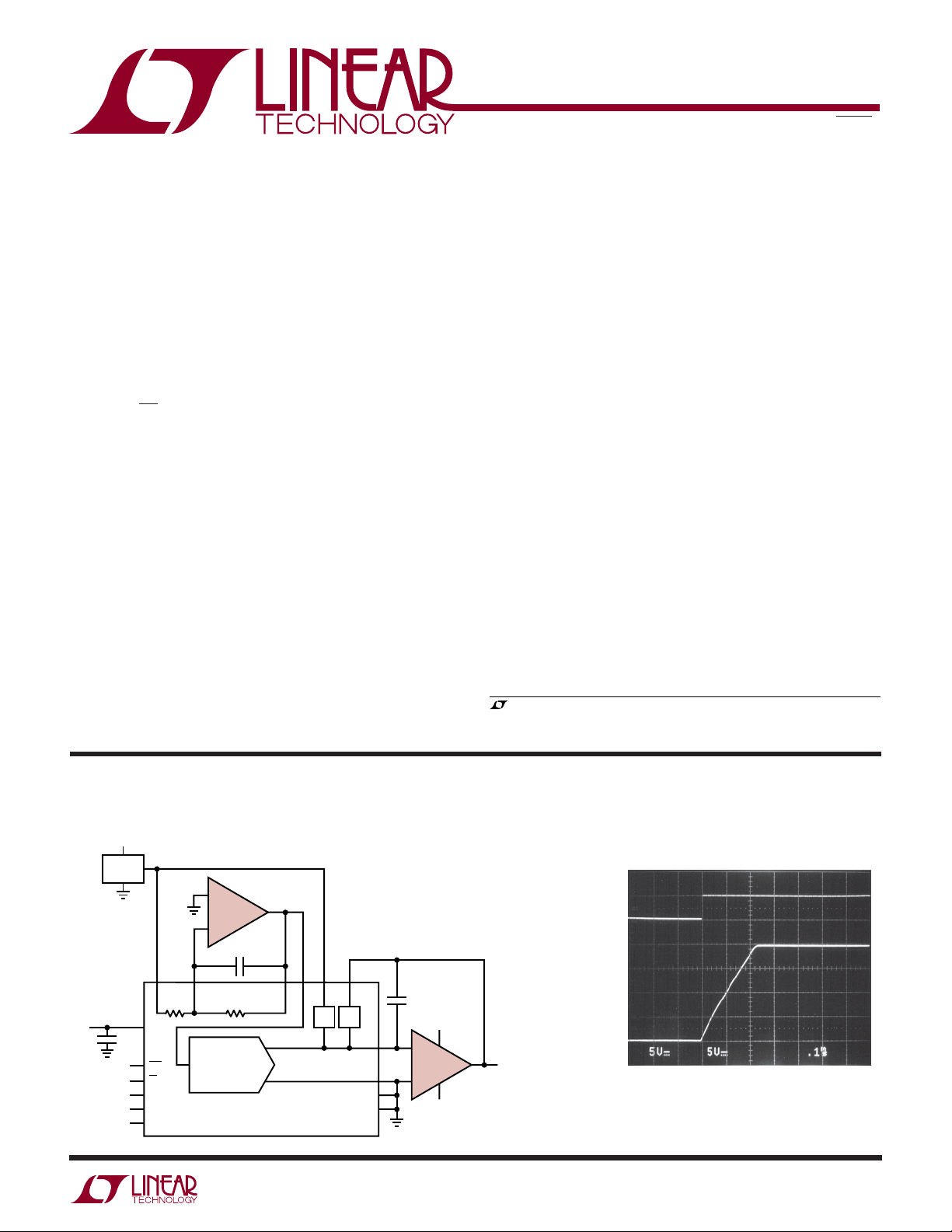
TYPICAL APPLICATIO
Low Power Programmable Output Range 16-Bit SoftSpanTM DAC
+
V
S
LT1236-5
5
+
1/2 LT6011
6
–
1
2
R
R1
COM
R1
9
0.1µF
V
CC
14
CLR
13
CS/LD
12
SCK
11
SDI
10
SDO
16-BIT DAC
5V
C2
270pF
R2
7
LTC1592
SUPPLY CURRENT ≅ 1.6mA TO 4mA
DEPENDING ON CODE
16
3
15
R2
REF
4
R
R
FB
OFS
I
5
OUT1
I
6
OUT2
7
AGND
8
GND
6011 TA01
C1
270pF
–
2
1/2 LT6011
3
+
20V Output Step Response
5V/DIV
0V
5V/DIV
0V
+
V
S
8
1
V
OUT
4
–
V
S
100µs/DIV
6011 TA03
60112fb
1
LT6011/LT6012
TOP VIEW
GN PACKAGE
16-LEAD PLASTIC SSOP
1
2
3
4
5
6
7
8
16
15
14
13
12
11
10
9
OUT A
–IN A
+IN A
V
+
+IN B
–IN B
OUT B
NC
OUT D
–IN D
+IN D
V
–
+IN C
–IN C
OUT C
NC
+
–
+
–
+
–
+
–
ABD
C
WWWU
ABSOLUTE AXI U RATI GS
(Note 1)
Total Supply Voltage (V+ to V–) .............................. 40V
Differential Input Voltage (Note 2) .......................... 10V
Input Voltage .................................................... V
+
to V
Input Current (Note 2) ....................................... ±10mA
Output Short-Circuit Duration (Note 3) ........... Indefinite
Operating Temperature Range (Note 4) .. – 40°C to 85°C
Specified Temperature Range (Note 5) ... –40°C to 85°C
UU
W
PACKAGE/ORDER I FOR ATIO
TOP VIEW
+
1OUT A
–IN A
2
A
+IN A
3
–
V
4
DD PACKAGE
8-LEAD (3mm × 3mm) PLASTIC DFN
T
= 125°C, θJA = 43°C/W
JMAX
UNDERSIDE METAL CONNECTED TO V
(PCB CONNECTION OPTIONAL)
ORDER PART
NUMBER
8
V
OUT B
7
–IN B
6
B
+IN B
5
–
DD
PART MARKING*
OUT A
1
–IN A
2
+IN A
3
–
V
4
8-LEAD PLASTIC SO
T
= 150°C, θJA = 190°C/W
JMAX
ORDER PART
NUMBER
Maximum Junction Temperature
DD Package ..................................................... 125°C
–
All Other Packages .......................................... 150°C
Storage Temperature Range
DD Package ..................................... – 65°C to 125°C
All Other Packages .......................... – 65°C to 150°C
Lead Temperature (Soldering, 10 sec)..................300°C
TOP VIEW
8
V
OUT B
A
S8 PACKAGE
7
–IN B
6
B
+IN B
5
PART MARKING
+
S8
OUT A
ORDER PART
NUMBER
TOP VIEW
1
–IN A
2
A
+IN A
3
–
V
4
MS8 PACKAGE
8-LEAD PLASTIC MSOP
T
= 150°C, θJA = 220°C/W
JMAX
V
8
7
OUT B
6
–IN B
B
5
+IN B
PART MARKING*
+
MS8
LT6011CDD
LT6011IDD
LT6011ACDD
LT6011AIDD
OUT A
–IN A
+IN A
+IN B
–IN B
OUT B
T
JMAX
LT6012CS
LT6012IS
Order Options
Lead Free: Add #PBF Lead Free Tape and Reel: Add #TRPBF
Lead Free Part Marking: http://www.linear.com/leadfree/
Consult LTC Marketing for parts specified with wider operating temperature ranges.
*Temperature grades are identified by a label on the shipping container.
2
Tape and Reel: Add #TR
LACD
LACD
LACD
LACD
TOP VIEW
1
2
–
ABD
+
3
+
4
V
+
5
–
6
7
14-LEAD PLASTIC SO
= 150°C, θJA = 110°C/W
C
S PACKAGE
14
OUT D
–
13
–IN D
+
12
+IN D
–
11
V
10
+IN C
+
–
9
–IN C
8
OUT C
LT6012ACS
LT6012AIS
LT6011CS8
LT6011IS8
LT6011ACS8
LT6011AIS8
6011
6011I
6011A
6011AI
LT6012CGN
LT6012IGN
LT6011CMS8
LT6011IMS8
T
= 150°C, θJA = 135°C/W
JMAX
LT6012ACGN
LT6012AIGN
GN PART MARKINGORDER PART NUMBERORDER PART NUMBER
6012
6012I
LTCGC
LTCGC
6012A
6012AI
60112fb
LT6011/LT6012
ELECTRICAL CHARACTERISTICS
temperature range, otherwise specifications are at T
The ● denotes the specifications which apply over the full operating
= 25°C. VS = 5V, 0V; VCM = 2.5V; RL to 0V; unless otherwise specified. (Note 5)
A
SYMBOL PARAMETER CONDITIONS MIN TYP MAX UNITS
V
OS
Input Offset Voltage (Note 8) LT6011AS8, LT6012AS 20 60 µV
T
= 0°C to 70°C
A
= –40°C to 85°C
T
A
●
●
85 µV
110 µV
LT6011ADD, LT6012AGN 25 85 µV
= 0°C to 70°C
T
A
T
= –40°C to 85°C
A
●
●
135 µV
170 µV
LT6011S8, LT6012S 25 75 µV
= 0°C to 70°C
T
A
= –40°C to 85°C
T
A
●
●
100 µV
125 µV
LT6011DD, LT6012GN, LT6011MS8 30 125 µV
T
= 0°C to 70°C
A
= –40°C to 85°C
T
A
∆VOS/∆T Input Offset Voltage Drift (Note 6) LT6011AS8, LT6011S8, LT6012AS,LT6012S
●
●
●
0.2 0.8 µV/°C
175 µV
210 µV
LT6011ADD,LT6011DD, LT6012AGN,
LT6012GN, LT6011MS8
I
OS
Input Offset Current (Note 8) LT6011AS8, LT6011ADD, LT6012AS,
●
0.2 1.2 µV/°C
LT6012AGN 20 300 pA
T
= 0°C to 70°C
A
= –40°C to 85°C
T
A
●
●
450 pA
600 pA
LT6011S8, LT6011DD, LT6012S,
LT6012GN, LT6011MS8 150 900 pA
= 0°C to 70°C
T
A
= –40°C to 85°C
T
A
I
B
Input Bias Current (Note 8) LT6011AS8, LT6011ADD, LT6012AS,
●
●
1200 pA
1500 pA
LT6012AGN 20 ±300 pA
= 0°C to 70°C
T
A
= –40°C to 85°C
T
A
●
●
±450 pA
±600 pA
LT6011S8, LT6011DD, LT6012S,
LT6012GN, LT6011MS8 150 ±900 pA
T
= 0°C to 70°C
A
= –40°C to 85°C
T
A
●
●
±1200 pA
±1500 pA
Input Noise Voltage 0.1Hz to 10Hz 400 nV
e
n
i
n
R
IN
Input Noise Voltage Density f = 1kHz 14 nV/√Hz
Input Noise Current Density f = 1kHz, Unbalanced Source Resistance 0.1 pA/√Hz
Input Resistance Common Mode, VCM = 1V to 3.8V 10 120 GΩ
Differential 20 MΩ
C
IN
V
CM
CMRR Common Mode Rejection Ratio VCM = 1V to 3.8V
PSRR Power Supply Rejection Ratio VS = 2.7V to 36V, VCM = 1/2V
A
VOL
Input Capacitance 4pF
Input Voltage Range (Positive) Guaranteed by CMRR
Input Voltage Range (Negative) Guaranteed by CMRR
Minimum Supply Voltage Guaranteed by PSRR
Large-Signal Voltage Gain RL = 10k, V
= 2k, V
R
L
Channel Separation V
= 1V to 4V
OUT
= 1V to 4V
OUT
= 1V to 4V
OUT
S
●
3.8 4 V
●
●
107 135 dB
●
●
112 135 dB
●
300 2000 V/mV
●
250 2000 V/mV
●
110 140 dB
0.7 1 V
2.4 2.7 V
P-P
60112fb
3
LT6011/LT6012
ELECTRICAL CHARACTERISTICS
temperature range, otherwise specifications are at T
The ● denotes the specifications which apply over the full operating
= 25°C. VS = 5V, 0V; VCM = 2.5V; RL to 0V; unless otherwise specified. (Note 5)
A
SYMBOL PARAMETER CONDITIONS MIN TYP MAX UNITS
V
OUT
Maximum Output Swing No Load, 50mV Overdrive 35 55 mV
(Positive, Referred to V
+
)
I
= 1mA, 50mV Overdrive 120 170 m V
SOURCE
●
●
65 mV
220 mV
Maximum Output Swing No Load, 50mV Overdrive 40 55 mV
(Negative, Referred to 0V)
I
= 1mA, 50mV Overdrive 150 225 m V
SINK
I
SC
Output Short-Circuit Current (Note 3) V
= 0V, 1V Overdrive, Source 10 14 mA
OUT
V
= 5V, –1V Overdrive, Sink 10 21 m A
OUT
●
●
●
4mA
●
4mA
65 mV
275 mV
SR Slew Rate AV = –10, RF = 50k, RG = 5k 0.06 0.09 V/µs
= 0°C to 70°C
T
A
T
= –40° C to 85°C
A
●
0.05 V/µs
●
0.04 V/µs
GBW Gain Bandwidth Product f = 10kHz 250 330 kHz
●
225 kHz
t
s
tr, t
∆V
f
OS
Settling Time AV = –1, 0.01%, V
= 1.5V to 3.5V 45 µs
OUT
Rise Time, Fall Time AV = 1, 10% to 90%, 0.1V Step 1 µs
Offset Voltage Match (Note 7) LT6011AS8, LT6012AS 50 120 µV
= 0°C to 70°C
T
A
T
= –40° C to 85°C
A
●
●
170 µV
220 µV
LT6011ADD, LT6012AGN 50 170 µV
T
= 0°C to 70°C
A
= –40° C to 85°C
T
A
●
●
270 µV
340 µV
LT6011S8, LT6012S 50 150 µV
= 0°C to 70°C
T
A
T
= –40° C to 85°C
A
●
●
200 µV
250 µV
LT6011DD, LT6012GN, LT6011MS8 60 250 µV
= 0°C to 70°C
T
A
= –40° C to 85°C
T
A
∆I
B
Input Bias Current Match (Note 7) LT6011AS8, LT6011ADD, LT6012AS,
●
●
350 µV
420 µV
LT6012AGN 50 600 pA
TA = 0°C to 70°C
= –40° C to 85°C
T
A
●
●
900 pA
1200 pA
LT6011S8, LT6011DD, LT6012S,
LT6012GN, LT6011MS8 1800 pA
∆CMRR Common Mode Rejection Ratio
= 0°C to 70°C
T
A
= –40° C to 85°C
T
A
●
●
●
101 135 dB
2400 p A
3000 pA
Match (Note 7)
∆PSRR Power Supply Rejection Ratio
●
106 135 dB
Match (Note 7)
I
S
Supply Current per Amplifier 135 150 µA
= 0°C to 70°C
T
A
= –40° C to 85°C
T
A
●
●
190 µA
210 µA
4
60112fb
LT6011/LT6012
ELECTRICAL CHARACTERISTICS
temperature range, otherwise specifications are at T
The ● denotes the specifications which apply over the full operating
= 25°C. VS = ±15V, VCM = 0V, RL to 0V, unless otherwise specified. (Note 5)
A
SYMBOL PARAMETER CONDITIONS MIN TYP MAX UNITS
V
OS
Input Offset Voltage (Note 8) LT6011AS8, LT6012AS 30 135 µV
= 0°C to 70°C
T
A
T
= –40°C to 85°C
A
●
●
160 µV
185 µV
LT6011ADD, LT6012AGN 35 160 µV
= 0°C to 70°C
T
A
= –40°C to 85°C
T
A
●
●
210 µV
225 µV
LT6011S8, LT6012S 35 150 µV
= 0°C to 70°C
T
A
= –40°C to 85°C
T
A
●
●
175 µV
200 µV
LT6011DD, LT6012GN, LT6011MS8 40 200 µV
= 0°C to 70°C
T
A
= –40°C to 85°C
T
A
∆VOS/∆T Input Offset Voltage Drift LT6011AS8, LT6011S8, LT6012AS, LT6012S
(Note 6) LT6011ADD, LT6011DD, LT6012AGN, LT6012GN, LT6011MS8
I
OS
Input Offset Current (Note 8) LT6011AS8, LT6011ADD, LT6012AS LT6012AGN 20 300 pA
= 0°C to 70°C
T
A
= –40°C to 85°C
T
A
●
●
●
●
●
●
0.2 0.8 µV/°C
0.2 1.3 µV/°C
250 µV
275 µV
450 pA
600 pA
LT6011S8, LT6011DD, LT6012S, LT6012GN, LT6011MS8 150 900 pA
= 0°C to 70°C
T
A
= –40°C to 85°C
T
A
I
B
Input Bias Current (Note 8) LT6011AS8, LT6011ADD, LT6012AS, LT6012AGN 20 ±300 pA
= 0°C to 70°C
T
A
= –40°C to 85°C
T
A
●
●
●
●
1200 p A
1500 pA
±450 p A
±600 pA
LT6011S8, LT6011DD, LT6012S, LT6012GN, LT6011MS8 150 ±900 pA
= 0°C to 70°C
T
A
= –40°C to 85°C
T
A
●
●
±1200 pA
±1500 pA
Input Noise Voltage 0.1Hz to 10Hz 400 nV
e
n
i
n
R
IN
Input Noise Voltage Density f = 1kHz 13 nV/√Hz
Input Noise Current Density f = 1kHz, Unbalanced Source Resistance 0.1 pA/√Hz
Input Resistance Common Mode, VCM = ±13.5V 50 400 GΩ
Differential 20 MΩ
C
IN
V
CM
Input Capacitance 4pF
Input Voltage Range Guaranteed by CMRR
●
±13.5 ±14 V
CMRR Common Mode Rejection VCM = –13.5V to 13.5V 115 135 dB
Ratio
Minimum Supply Voltage Guaranteed by PSRR
PSRR Power Supply Rejection Ratio VS = ±1.35V to ±18V
A
VOL
V
OUT
Large-Signal Voltage Gain RL = 10k, V
RL = 5k, V
Channel Separation V
Maximum Output Swing No Load, 50mV Overdrive 45 80 mV
(Positive, Referred to V
Maximum Output Swing No Load, 50mV Overdrive 45 80 mV
(Negative, Referred to V
+
)
–
)
= –13.5V to 13.5V
OUT
I
SOURCE
I
= 1mA, 50mV Overdrive 150 250 m V
SINK
= –13.5V to 13.5V 1000 2000 V/mV
OUT
= –13.5V to 13.5V 500 1500 V/mV
OUT
= 1mA, 50mV Overdrive 140 195 m V
●
112 135 dB
●
●
112 135 dB
●
600 V/mV
●
300 V/mV
●
120 140 dB
●
●
●
●
±1.2 ±1.35 V
100 mV
240 mV
100 mV
300 mV
P-P
60112fb
5

LT6011/LT6012
ELECTRICAL CHARACTERISTICS
temperature range, otherwise specifications are at T
The ● denotes the specifications which apply over the full operating
= 25°C. VS = ±15V, VCM = 0V, RL to 0V, unless otherwise specified. (Note 5)
A
SYMBOL PARAMETER CONDITIONS MIN TYP MAX UNITS
I
SC
Output Short-Circuit Current V
(Note 3)
= 0V, 1V Overdrive (Source) 10 15 mA
OUT
V
= 0V, –1V Overdrive (Sink) 10 20 mA
OUT
●
5mA
●
5mA
SR Slew Rate AV = –10, RF = 50k, RG = 5k 0.08 0.11 V/µs
= 0°C to 70°C
T
A
= –40° C to 85°C
T
A
●
0.07 V/µs
●
0.05 V/µs
GBW Gain Bandwidth Product f = 10kHz 275 350 kHz
●
250 kHz
t
s
tr, t
∆V
f
OS
Settling Time AV = –1, 0.01%, V
= 0V to 10V 85 µs
OUT
Rise Time, Fall Time AV = 1, 10% to 90%, 0.1V Step 1 µs
Offset Voltage Match (Note 7) LT6011AS8, LT6012AS 50 270 µV
T
= 0°C to 70°C
A
= –40° C to 85°C
T
A
●
●
320 µV
370 µV
LT6011ADD, LT6012AGN 50 320 µV
= 0°C to 70°C
T
A
= –40° C to 85°C
T
A
●
●
420 µV
450 µV
LT6011S8, LT6012S 70 300 µV
T
= 0°C to 70°C
A
= –40° C to 85°C
T
A
●
●
350 µV
400 µV
LT6011DD, LT6012GN, LT6011MS8 80 400 µV
= 0°C to 70°C
T
A
= –40° C to 85°C
T
A
∆I
B
Input Bias Current Match (Note 7) LT6011AS8, LT6011ADD, LT6012AS, LT6012AGN 50 600 pA
= 0°C to 70°C
T
A
= –40° C to 85°C
T
A
●
●
●
●
500 µV
550 µV
900 pA
1200 pA
LT6011S8, LT6011DD, LT6012S, LT6012GN,
LT6011MS8 1800 pA
T
∆CMRR Common Mode Rejection Ratio
= 0°C to 70°C
A
= –40° C to 85°C
T
A
●
●
●
109 135 dB
2400 pA
3000 pA
Match (Note 7)
∆PSRR Power Supply Rejection Ratio
●
106 135 dB
Match (Note 7)
I
S
Note 1: Stresses beyond those listed under Absolute Maximum Ratings
may cause permanent damage to the device. Exposure to any Absolute
Maximum Rating condition for extended periods may affect device
reliability and lifetime.
Note 2: The inputs are protected by back-to-back diodes and internal
series resistors. If the differential input voltage exceeds 10V, the input
current must be limited to less than 10mA.
Note 3: A heat sink may be required to keep the junction temperature
below absolute maximum ratings.
Note 4: Both the LT6011C/LT6012C and LT6011I/LT6012I are guaranteed
functional over the operating temperature range of – 40°C to 85°C.
Note 5: The LT6011C/LT6012C are guaranteed to meet the specified
performance from 0°C to 70°C and is designed, characterized and
expected to meet specified performance from –40°C to 85°C but is not
tested or QA sampled at these temperatures. The LT6011I/LT6012I are
guaranteed to meet specified performance from –40°C to 85°C.
Supply Current per Amplifier 260 330 µA
= 0°C to 70°C
T
A
TA = –40° C to 85°C
●
●
380 µA
400 µA
Note 6: This parameter is not 100% tested.
Note 7: Matching parameters are the difference between any two
amplifiers. ∆CMRR and ∆PSRR are defined as follows: (1) CMRR and
PSRR are measured in µV/V for the individual amplifiers. (2) The
difference between matching amplifiers is calculated in µV/V. (3) The
result is converted to dB.
Note 8: The specifications for V
, IB, and IOS depend on the grade and on
OS
the package. The following table clarifies the notations.
STANDARD GRADE A GRADE
S8 Package LT6011S8 LT6011AS8
DFN Package LT6011DD LT6011ADD
S14 Package LT6012S LT6012AS
GN16 Package LT6012GN LT6012AGN
MS8 Package LT6011MS8 N/A
60112fb
6

UW
INPUT COMMON MODE VOLTAGE (V)
–15
120
100
80
60
40
20
0
–20
010
6011 G03
–10 –5
515
OFFSET VOLTAGE (µV)
TA = 85°C
TA = 25°C
TA = –40°C
V
S
= ±15V
TYPICAL PART
COMMON MODE VOLTAGE (V)
–15
–200
INPUT BIAS CURRENT (pA)
–100
0
100
200
300
–10
–5 0 5
1635 G06
10 15
VS = ±15V
TYPICAL PART
TA = 85°C
13.9V
–14.2V
TA = 25°C
TA = –40°C
TYPICAL PERFOR A CE CHARACTERISTICS
LT6011/LT6012
Distribution of Input Offset Voltage
30
VS = 5V, 0V
= 25°C
T
A
25
20
15
10
PERCENT OF UNITS (%)
5
0
–70 –30
–50
–90
INPUT OFFSET VOLTAGE (µV)
10 90
–10
30
Distribution of Input Bias Current
25
VS = 5V, 0V
= 25°C
T
A
20
15
10
PERCENT OF UNITS (%)
5
0
–400
–200
–300
INPUT BIAS CURRENT (pA)
–100
LT6011A,
LT6012A
200
0 400
100
LT6011S8,
LT6012S
50
70
6011 G01
300
6011 G04
Input Offset Voltage
vs Temperature
125
VS = 5V, 0V
100
REPRESENTATIVE UNITS
75
50
25
0
–25
–50
OFFSET VOLTAGE (µV)
–75
–100
–125
–50
0
–25
TEMPERATURE (°C)
50
25
Input Bias Current vs Temperature
1600
VS = 5V, 0V
TYPICAL PART
1400
1200
1000
800
600
400
200
INPUT BIAS CURRENT (pA)
0
–200
–50
–25
–
I
B
+
I
B
0
25
TEMPERATURE (°C)
50
75
100
75 100
Offset Voltage
vs Input Common Mode Voltage
125
6011 G02
Input Bias Current
vs Input Common Mode Voltage
125
6011 G05
e
n
100 100
INPUT VOLTAGE NOISE DENSITY (nV/√Hz)
10
1
, in vs Frequency
CURRENT NOISE
UNBALANCED
SOURCE RESISTORS
VOLTAGE NOISE
10 100 1000
FREQUENCY (Hz)
VS = ±15V
= 25°C
T
A
6011 G07
1000
INPUT CURRENT NOISE DENSITY (fA/√Hz)
Total Input Noise
vs Source Resistance
10
VS = 5V, 0V
= 25°C
T
A
f = 1kHz
1
UNBALANCED
SOURCE RESISTORS
0.1
TOTAL NOISE
0.01
RESISTOR NOISE ONLY
0.001
TOTAL INPUT NOISE (µV/√Hz)
0.0001
100 1k 10k 100k 1M 10M
SOURCE RESISTANCE (Ω)
6011 G08
100M
0.1Hz to 10Hz Noise
VS = ±15V
= 25°C
T
A
NOISE VOLTAGE (0.2µV/DIV)
246 107135 9
0
TIME (SEC)
8
6011 G09
60112fb
7

LT6011/LT6012
SETTLING TIME (µs)
0
0
OUTPUT STEP (V)
2
6
8
10
20
40
50 90
6011 G18
4
10 30
60
70
80
VS = ±15V
A
V
= 1
0.1%
0.01%
UW
TYPICAL PERFOR A CE CHARACTERISTICS
0.01Hz to 1Hz Noise
VS = ±15V
= 25°C
T
A
NOISE VOLTAGE (0.2µV/DIV)
20 40 60 1007010 30 50 90
0
TIME (SEC)
Output Saturation Voltage
vs Load Current (Output Low)
1
VS = 5V, 0V
TA = 85°C
TA = 25°C
0.1
TA = –40°C
OUTPUT LOW SATURATION VOLTAGE (V)
0.01
0.01
0.1 1 10
LOAD CURRENT (mA)
Output Voltage Swing
vs Temperature
+
V
–20
–40
–60
60
40
OUTPUT VOLTAGE SWING (mV)
20
–
80
6011 G10
V
–25 0 50
–50
OUTPUT HIGH
OUTPUT LOW
25
TEMPERATURE (°C)
VS = 5V, 0V
NO LOAD
75 100 125
6011 G11
Supply Current vs Supply Voltage
500
PER AMPLIFIER
450
400
6011 G13
350
300
250
200
150
SUPPLY CURRENT (µA)
100
50
0
0
TA = 25°C
42
SUPPLY VOLTAGE (±V)
86
10
TA = 85°C
TA = –40°C
12 14 18
16
20
6011 G14
Output Saturation Voltage
vs Load Current (Output High)
1
VS = 5V, 0V
TA = 85°C
TA = 25°C
0.1
TA = –40°C
OUTPUT HIGH SATURATION VOLTAGE (V)
0.01
0.01
0.1 1 10
LOAD CURRENT (mA)
Warm-Up Drift
3
2
1
CHANGE IN OFFSET VOLTAGE (µV)
0
30 60 90 120
TIME AFTER POWER-ON (SECONDS)
±15V
±2.5V
6011 G12
150
6011 G15
THD + NOISE (%)
0.0001
8
THD + Noise vs Frequency
10
VS = 5V, 0V
= 2V
V
OUT
P-P
TA = 25°C
1
= 1: RL = 10k
A
V
= –1: RF = RG = 10k
A
V
0.1
0.01
0.001
10
AV = –1
FREQUENCY (Hz)
AV = 1
1k 10k100 100k
6011 G16
THD + Noise vs Frequency Settling Time vs Output Step
10
VS = ±15V
= 20V
V
IN
P-P
TA = 25°C
1
0.1
0.01
THD + NOISE (%)
0.001
0.0001
10
AV = –1
AV = 1
1k 10k100
FREQUENCY (Hz)
6011 G17
60112fb

UW
FREQUENCY (Hz)
110
40
COMMON MODE REJECTION RATIO (dB)
60
80
100
120
100 1k 10k 100k 1M
6011 G21
20
0
140
160
TA = 25°C
VS = ±15V
VS = 5V, 0V
TYPICAL PERFOR A CE CHARACTERISTICS
LT6011/LT6012
Settling Time vs Output Step
10
VS = ±15V
= –1
A
V
8
6
4
OUTPUT STEP (V)
2
0
10 30
0
0.1%
20
40
SETTLING TIME (µs)
50 90
0.01%
60
70
80
6011 G19
Channel Separation vs Frequency CMRR vs Frequency
160
140
120
100
80
60
40
CHANNEL SEPARATION (dB)
20
0
110
100 1k 10k 100k 1M
FREQUENCY (Hz)
VS = 5V, 0V
= 25°C
T
A
6011 G20
PSRR vs Frequency Output Impedance vs Frequency Open-Loop Gain vs Frequency
140
120
100
80
60
40
20
POWER SUPPLY REJECTION RATIO (dB)
0
1 10 100 1k 10k 100k 1M
0.1
FREQUENCY (Hz)
+PSRR
–PSRR
VS = 5V, 0V
= 25°C
T
A
6011 G22
1000
VS = 5V, 0V
= 25°C
T
A
100
10
AV = 100
1
AV = 10
OUTPUT IMPEDANCE (Ω)
0.1
AV = 1
0.01
1 100 1k 10k 100k 1M
10
FREQUENCY (Hz)
6011 G23
140
120
100
80
60
40
20
OPEN-LOOP GAIN (dB)
0
–20
–40
0.1 1
0.01 10 100 1k 10k 100k 1M 10M
FREQUENCY (Hz)
VS = 5V, 0V
= 25°C
T
A
= 10k
R
L
6011 G24
Gain and Phase vs Frequency
60
50
40
30
20
10
0
–10
OPEN-LOOP GAIN (dB)
–20
–30
–40
1k 100k 1M 10M
10k
FREQUENCY (Hz)
GAIN
PHASE
VS = 5V, 0V
= 25°C
T
A
= 10k
R
L
6011 G25
–80
–120
PHASE SHIFT (DEG)
–160
–200
–240
–280
Gain vs Frequency, A
10
VS = 5V, 0V
= 25°C
T
A
5
0
–5
GAIN (dB)
–10
–15
–20
1k
10k 100k 1M
V
CL = 500pF
CL = 50pF
FREQUENCY (Hz)
= 1
6011 G26
Gain vs Frequency, AV = –1
10
VS = 5V, 0V
= 25°C
T
A
5
0
–5
GAIN (dB)
–10
–15
–20
1k
10k 100k 1M
FREQUENCY (Hz)
CL = 500pF
CL = 50pF
6011 G27
60112fb
9

LT6011/LT6012
UW
TYPICAL PERFOR A CE CHARACTERISTICS
Small-Signal Transient Response Large-Signal Transient Response Rail-to-Rail Output Swing
5V
20mV/DIV
A
= 1 2µs/DIV
V
6011 G28
2V/DIV
A
= –1 50µs/DIV
V
VS = ±15V
WUUU
APPLICATIO S I FOR ATIO
Preserving Input Precision
Preserving the input accuracy of the LT6011/LT6012 requires that the applications circuit and PC board layout do
not introduce errors comparable to or greater than the 25µV
typical offset of the amplifiers. Temperature differentials
across the input connections can generate thermocouple
voltages of 10’s of microvolts so the connections to the input
leads should be short, close together and away from heat
dissipating components. Air currents across the board can
also generate temperature differentials.
The extremely low input bias currents (20pA typical) allow
high accuracy to be maintained with high impedance
sources and feedback resistors. The LT6011
/LT6012
input bias currents are obtained by a cancellation circuit
+
on-chip. This causes the resulting I
uncorrelated, as implied by the I
comparable to I
. Do not try to balance the input resistances
B
OS
and I
B
specification being
in each input lead; instead keep the resistance at either input
as low as possible for maximum accuracy.
Leakage currents on the PC board can be higher than the
input bias current. For example, 10GΩ of leakage between
a 15V supply lead and an input lead will generate 1.5nA!
Surround the input leads with a guard ring driven to the
same potential as the input common mode to avoid excessive leakage in high impedance applications.
Input Protection
The LT6011/LT6012 feature on-chip back-to-back diodes
between the input devices, along with 500Ω resistors in
–
B
low
to be
1V/DIV
0V
0V
6011 G29
A
= –1 100µs/DIV
V
VS = 5V, 0V
6011 G30
series with either input. This internal protection limits the
input current to approximately 10mA (the maximum allowed) for a 10V differential input voltage. Use additional
external series resistors to limit the input current to 10mA
in applications where differential inputs of more than 10V
are expected. For example, a 1k resistor in series with each
input provides protection against 30V differential voltage.
Input Common Mode Range
The LT6011/LT6012 output is able to swing close to each
power supply rail (rail-to-rail out), but the input stage is
limited to operating between V
–
+ 1V and V+ – 1.2V. Exceeding this common mode range will cause the gain to drop
to zero, however, no phase reversal will occur.
Total Input Noise
The LT6011/LT6012 amplifier contributes negligible noise
to the system when driven by sensors (sources) with
impedance between 20kΩ and 1MΩ. Throughout this
range, total input noise is dominated by the 4kTR
noise
S
of the source. If the source impedance is less than 20kΩ,
the input voltage noise of the amplifier starts to contribute
with a minimum noise of 14nV/√Hz for very low source impedance. If the source impedance is more than 1MΩ, the
input current noise of the amplifier, multiplied by this high
impedance, starts to contribute and eventually dominate.
Total input noise spectral density can be calculated as:
v e kTR i R
n TOTAL n S n S()
2
4
()=+ +
2
60112fb
10

WUUU
APPLICATIO S I FOR ATIO
LT6011/LT6012
where en = 14nV/√Hz , in = 0.1pA/√Hz and RS is the total
impedance at the input, including the source impedance.
Capacitive Loads
The LT6011/LT6012 can drive capacitive loads up to 500pF
in unity gain. The capacitive load driving capability increases
as the amplifier is used in higher gain configurations. A small
series resistance between the output and the load further
increases the amount of capacitance that the amplifier can
drive.
V
REF
R
G
V
IN
INVERTING: A
OP AMP INPUTS DO NOT MOVE,
BUT ARE FIXED AT DC BIAS
POINT V
REF
INPUT DOES NOT HAVE TO BE
RAIL-TO-RAIL
+
–
= –RF/R
V
V
IN
R
F
G
+
–
R
G
V
REF
NONINVERTING: AV = 1 + RF/R
INPUTS MOVE BY AS MUCH AS
, BUT THE OUTPUT MOVES
V
IN
MORE
INPUT MAY NOT HAVE TO BE
RAIL-TO-RAIL
Rail-to-Rail Operation
The LT6011/LT6012 outputs can swing to within millivolts
of either supply rail, but the inputs can not. However, for
most op amp configurations, the inputs need to swing less
than the outputs. Figure 1 shows the basic op amp configurations, lists what happens to the op amp inputs and specifies whether or not the op amp must have rail-to-rail inputs.
Select a rail-to-rail input op amp only when really necessary, because the input precision specifications are usually
inferior.
V
IN
R
F
G
+
–
NONINVERTING: A
INPUTS MOVE BY AS MUCH AS
OUTPUT
INPUT MUST BE RAIL-TO-RAIL
FOR OVERALL CIRCUIT
RAIL-TO-RAIL PERFORMANCE
= 1
V
6011 F01
Figure 1. Some Op Amp Configurations Do Not Require Rail-to-Rail Inputs to Achieve Rail-to-Rail Outputs
WW
SI PLIFIED SCHE ATIC
+
V
R3 R4
Q7
Q3
R1
500Ω
–IN
+IN
R2
500Ω
Q1 Q2
(One Amplifier)
Q8
Q4
D2D1
Q17
Q21
C
B
A
Q11
Q13
Q14
Q18
R6
Q19
OUT
C3
Q20
R5
Q6
C1
R
Q12
C1
D3
D4
D5
Q5
C2
Q16
Q22
Q15
Q9
Q10
B
A
–
V
6011 SS
60112fb
11

LT6011/LT6012
PACKAGE DESCRIPTIO
U
DD Package
8-Lead Plastic DFN (3mm × 3mm)
(Reference LTC DWG # 05-08-1698)
3.5 ±0.05
0.675 ±0.05
1.65 ±0.05
(2 SIDES)2.15 ±0.05
PACKAGE
OUTLINE
0.25 ± 0.05
RECOMMENDED SOLDER PAD PITCH AND DIMENSIONS
2.38 ±0.05
(2 SIDES)
0.50
BSC
8-Lead Plastic Small Outline (Narrow .150 Inch)
PIN 1
TOP MARK
(NOTE 6)
0.200 REF
NOTE:
1. DRAWING TO BE MADE A JEDEC PACKAGE OUTLINE M0-229 VARIATION OF (WEED-1)
2. DRAWING NOT TO SCALE
3. ALL DIMENSIONS ARE IN MILLIMETERS
4. DIMENSIONS OF EXPOSED PAD ON BOTTOM OF PACKAGE DO NOT INCLUDE
MOLD FLASH. MOLD FLASH, IF PRESENT, SHALL NOT EXCEED 0.15mm ON ANY SIDE
5. EXPOSED PAD SHALL BE SOLDER PLATED
6. SHADED AREA IS ONLY A REFERENCE FOR PIN 1 LOCATION
ON TOP AND BOTTOM OF PACKAGE
S8 Package
(Reference LTC DWG # 05-08-1610)
3.00 ±0.10
(4 SIDES)
0.75 ±0.05
1.65 ± 0.10
0.00 – 0.05
R = 0.115
(2 SIDES)
0.25 ± 0.05
BOTTOM VIEW—EXPOSED PAD
TYP
2.38 ±0.10
(2 SIDES)
0.38 ± 0.10
85
14
0.50 BSC
(DD8) DFN 1203
.050 BSC
.245
MIN
.030
±
.005
TYP
RECOMMENDED SOLDER PAD LAYOUT
.010 – .020
(0.254 – 0.508)
.008 – .010
(0.203 – 0.254)
NOTE:
1. DIMENSIONS IN
2. DRAWING NOT TO SCALE
3. THESE DIMENSIONS DO NOT INCLUDE MOLD FLASH OR PROTRUSIONS.
MOLD FLASH OR PROTRUSIONS SHALL NOT EXCEED .006" (0.15mm)
× 45°
.016 – .050
(0.406 – 1.270)
INCHES
(MILLIMETERS)
.045 ±.005
±
.005
.160
0°– 8° TYP
.228 – .244
(5.791 – 6.197)
.053 – .069
(1.346 – 1.752)
.014 – .019
(0.355 – 0.483)
TYP
(4.801 – 5.004)
8
1
.189 – .197
NOTE 3
7
2
5
6
.150 – .157
(3.810 – 3.988)
NOTE 3
3
4
.004 – .010
(0.101 – 0.254)
.050
(1.270)
BSC
SO8 0303
60112fb
12

PACKAGE DESCRIPTIO
U
MS8 Package
8-Lead Plastic MSOP
(Reference LTC DWG # 05-08-1660)
0.889 ± 0.127
(.035 ± .005)
LT6011/LT6012
5.23
(.206)
MIN
0.42 ± 0.038
(.0165 ± .0015)
TYP
RECOMMENDED SOLDER PAD LAYOUT
0.254
(.010)
GAUGE PLANE
0.18
(.007)
NOTE:
1. DIMENSIONS IN MILLIMETER/(INCH)
2. DRAWING NOT TO SCALE
3. DIMENSION DOES NOT INCLUDE MOLD FLASH, PROTRUSIONS OR GATE BURRS.
MOLD FLASH, PROTRUSIONS OR GATE BURRS SHALL NOT EXCEED 0.152mm (.006") PER SIDE
4. DIMENSION DOES NOT INCLUDE INTERLEAD FLASH OR PROTRUSIONS.
INTERLEAD FLASH OR PROTRUSIONS SHALL NOT EXCEED 0.152mm (.006") PER SIDE
5. LEAD COPLANARITY (BOTTOM OF LEADS AFTER FORMING) SHALL BE 0.102mm (.004") MAX
DETAIL “A”
(.126 – .136)
(.0256)
° – 6° TYP
0
DETAIL “A”
3.20 – 3.45
0.65
BSC
0.53 ± 0.152
(.021 ± .006)
SEATING
PLANE
3.00 ± 0.102
(.118 ± .004)
(NOTE 3)
4.90 ± 0.152
(.193 ± .006)
0.22 – 0.38
(.009 – .015)
TYP
1.10
(.043)
MAX
8
12
0.65
(.0256)
BSC
7
6
3
5
4
0.52
(.0205)
REF
3.00 ± 0.102
(.118 ± .004)
(NOTE 4)
0.86
(.034)
REF
0.127 ± 0.076
(.005 ± .003)
MSOP (MS8) 0204
60112fb
13

LT6011/LT6012
PACKAGE DESCRIPTIO
U
S14 Package
14-Lead Plastic Small Outline (Narrow .150 Inch)
(Reference LTC DWG # 05-08-1610)
.050 BSC
N
.245
MIN
123 N/2
.030 ±.005
TYP
RECOMMENDED SOLDER PAD LAYOUT
.010 – .020
(0.254 – 0.508)
.008 – .010
(0.203 – 0.254)
NOTE:
1. DIMENSIONS IN
2. DRAWING NOT TO SCALE
3. THESE DIMENSIONS DO NOT INCLUDE MOLD FLASH OR PROTRUSIONS.
MOLD FLASH OR PROTRUSIONS SHALL NOT EXCEED .006" (0.15mm)
×
°
45
.016 – .050
(0.406 – 1.270)
INCHES
(MILLIMETERS)
.045 ±.005
.160 ±.005
.228 – .244
(5.791 – 6.197)
0° – 8° TYP
.053 – .069
(1.346 – 1.752)
.014 – .019
(0.355 – 0.483)
TYP
.337 – .344
(8.560 – 8.738)
NOTE 3
13
12
11
4
10
.050
(1.270)
BSC
5
14
N
1
3
2
8
9
.150 – .157
(3.810 – 3.988)
N/2
7
6
NOTE 3
.004 – .010
(0.101 – 0.254)
S14 0502
14
60112fb

PACKAGE DESCRIPTIO
LT6011/LT6012
U
GN Package
16-Lead Plastic SSOP (Narrow .150 Inch)
(Reference LTC DWG # 05-08-1641)
.045 ±.005
.254 MIN
RECOMMENDED SOLDER PAD LAYOUT
.007 – .0098
(0.178 – 0.249)
.016 – .050
NOTE:
1. CONTROLLING DIMENSION: INCHES
2. DIMENSIONS ARE IN
3. DRAWING NOT TO SCALE
*DIMENSION DOES NOT INCLUDE MOLD FLASH. MOLD FLASH
SHALL NOT EXCEED 0.006" (0.152mm) PER SIDE
**DIMENSION DOES NOT INCLUDE INTERLEAD FLASH. INTERLEAD
FLASH SHALL NOT EXCEED 0.010" (0.254mm) PER SIDE
(0.406 – 1.270)
INCHES
(MILLIMETERS)
.150 – .165
.0250 BSC.0165 ± .0015
.015 ± .004
(0.38
0° – 8° TYP
± 0.10)
× 45°
.229 – .244
(5.817 – 6.198)
.0532 – .0688
(1.35 – 1.75)
.008 – .012
(0.203 – 0.305)
TYP
16
15
12
.189 – .196*
(4.801 – 4.978)
14
12 11 10
13
5
4
3
678
9
.004 – .0098
(0.102 – 0.249)
.0250
(0.635)
BSC
.009
(0.229)
REF
.150 – .157**
(3.810 – 3.988)
GN16 (SSOP) 0204
Information furnished by Linear Technology Corporation is believed to be accurate and reliable.
However, no responsibility is assumed for its use. Linear Technology Corporation makes no representation that the interconnection of its circuits as described herein will not infringe on existing patent rights.
60112fb
15

LT6011/LT6012
TYPICAL APPLICATIO
V
S
4
LT1790-1.25
= 3V TO 18V
V
S
= ~600µA
I
S
V
OUT
6
1, 2
7.87k
= ~40mV/mT
1%
100k
1%
U
Low Power Hall Sensor Amplifier
HALL ELEMENT
ASAHI-KASEI
HW-108A (RANK D)
www.asahi-kasei.co.jp
1
10k
+
LT1782
–
V
S
OFFSET
ADJUST
400Ω
3
26.7k
1%
V
S
3
2
2
×4
1k
4
6
5
+
1/2 LT6011
–
–
1/2 LT6011
+
8
49.9k
49.9k
4
6011 TA02
1
V
OUT
7
RELATED PARTS
PART NUMBER DESCRIPTION COMMENTS
LT1112/LT1114 Dual/Quad Low Power, Picoamp Input Precision Op Amp 250pA Input Bias Current
LT1880 Rail-to-Rail Output, Picoamp Input Precision Op Amp SOT-23
LT1881/LT1882 Dual/Quad Rail-to-Rail Output, Picoamp Input Precision Op Amp C
LT1884/LT1885 Dual/Quad Rail-to-Rail Output, Picoamp Input Precision Op Amp 9.5nV/√Hz Input Noise
LT1991/LT1996 Precision, 100µA Gain-Selectable Amplifier LT6011-Like Op Amp with 0.04% Matched Resistors
LT6010 Single 135µA, 14nV/√Hz Rail-to-Rail Output Precision Op Amp 35µV Maximum VOS; 100pA Maximum IB; Shutdown
LT6013/LT6014 Single/Dual 145µA, 9.5nV/√Hz, Rail-to-Rail Output Precision AV ≥ 5 Stable; 1.4MHz GBW
Op Amp
Up to 1000pF
LOAD
16
Linear Technology Corporation
1630 McCarthy Blvd., Milpitas, CA 95035-7417
(408) 432-1900 ● FAX: (408) 434-0507
●
www.linear.com
60112fb
LT 0406 REV B • PRINTED IN USA
© LINEAR TECHNOLOGY CORPORATION 2003
 Loading...