

FEATURES
■
35µV Maximum Offset Voltage
■
110pA Maximum Input Bias Current
■
135µA Supply Current
■
Rail-to-Rail Output Swing
■
12µA Supply Current in Shutdown
■
120dB Minimum Voltage Gain (VS = ±15V)
■
0.8µV/°C Maximum VOS Drift
■
14nV/√Hz Input Noise Voltage
■
2.7V to ±18V Supply Voltage Operation
■
Operating Temperature Range: –40°C to 85°C
■
Space Saving 3mm × 3mm DFN Package
U
APPLICATIO S
■
Thermocouple Amplifiers
■
Precision Photo Diode Amplifiers
■
Instrumentation Amplifiers
■
Battery-Powered Precision Systems
LT6010
135µA, 14nV/√Hz,
Rail-to-Rail Output Precision
Op Amp with Shutdown
U
DESCRIPTIO
The LT®6010 op amp combines low noise and high precision input performance with low power consumption and
rail-to-rail output swing.
Input offset voltage is trimmed to less than 35µV. The low
drift and excellent long-term stability guarantee a high
accuracy over temperature and over time. The 110pA
maximum input bias current and 120dB minimum voltage
gain further maintain this precision over operating
conditions.
The LT6010 works on any power supply voltage from 2.7V
to 36V, and draws only 135µA of supply current on a 5V
supply. A power saving shutdown feature reduces supply
current to 12µA. The output voltage swings to within
40mV of either supply rail, making the amplifier a good
choice for low voltage single supply operation.
The LT6010 is fully specified at 5V and ±15V supplies and
from –40°C to 85°C. The device is available in SO-8 and
space-saving 3mm × 3mm DFN packages. This op amp
is also available in dual (LT6011) and quad (LT6012)
packages.
, LTC and LT are registered trademarks of Linear Technology Corporation.
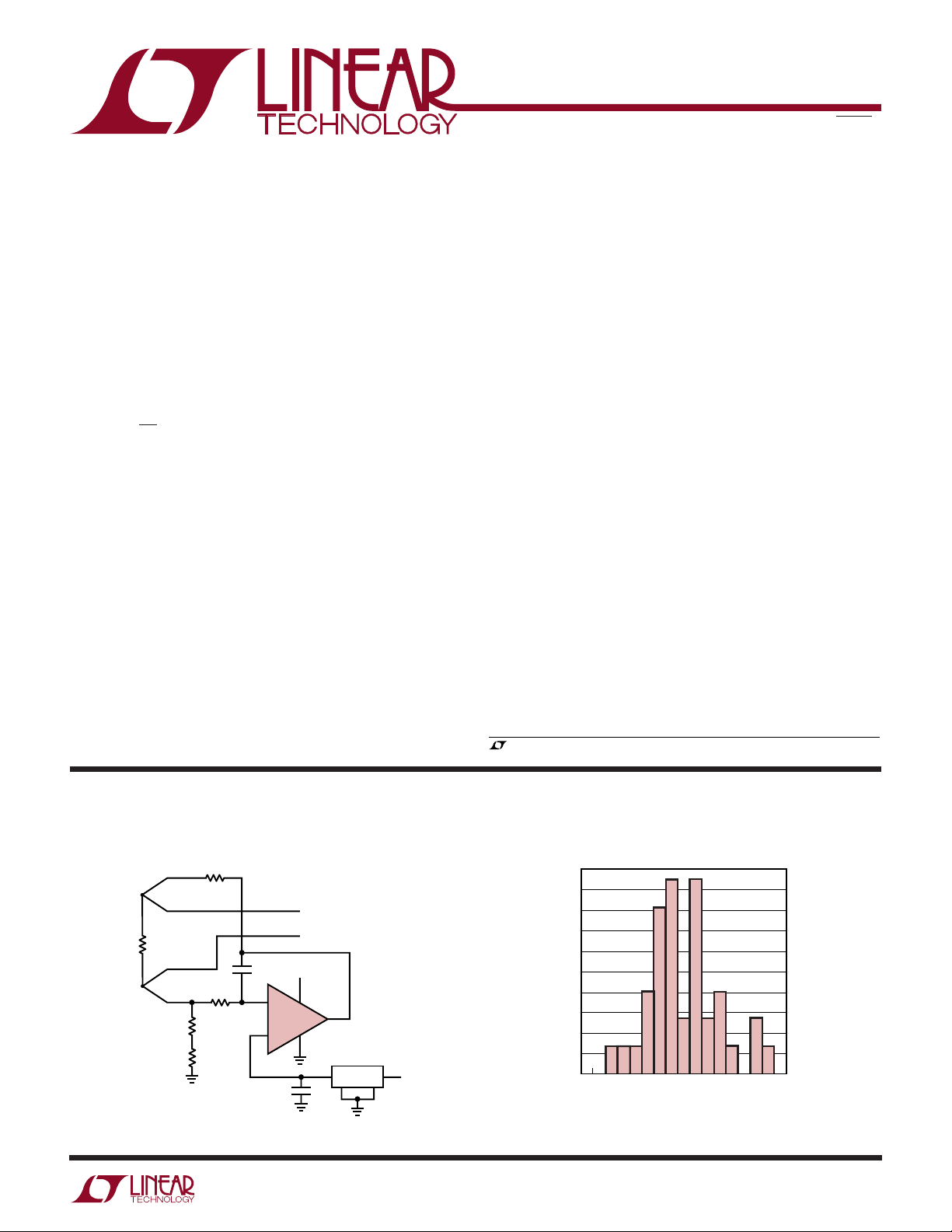
TYPICAL APPLICATIO
Single Supply Current Source for Platinum RTD
R5
1k, 5%
1k
AT 0°C
RTD*
R1
12.4k
0.1%
R2
100Ω
1%
VS = 2.7V TO 20V
≈ 320µA
I
CC
*OMEGA F3141 1kΩ, 0.1% PLATINUM RTD (800) 826-6342
R4
1k, 5%
C1
0.1µF
2
3
–
+
LT6010
U
+
= 100mV AT 0°C + 385µV/°C
V
OUT
–50°C TO 600°C
–
V
S
7
6
4
64
LT1790-1.25
1µF
1
2
6010 TA01a
Distribution of Offset Voltage Drift
20
VS = ±2.5V SO-8 PACKAGES
18
16
14
12
10
8
6
PERCENTAGE OF UNITS (%)
4
2
V
S
0
–0.8 –0.6 –0.4 –0.2
DISTRIBUTION (µV/°C)
0.4 0.6 0.80.2
0
6010 TA01b
sn6010 6010fs
1
LT6010
WWWU
ABSOLUTE AXI U RATI GS
(Note 1)
Total Supply Voltage (V+ to V–) .............................. 40V
Differential Input Voltage (Note 2) .......................... 10V
Input Voltage, Shutdown Voltage ..................... V+ to V
–
Input Current (Note 2) ....................................... ±10mA
Output Short-Circuit Duration (Note 3)........... Indefinite
Operating Temperature Range (Note 4) .. – 40°C to 85°C
Specified Temperature Range (Note 5)... –40°C to 85°C
UU
W
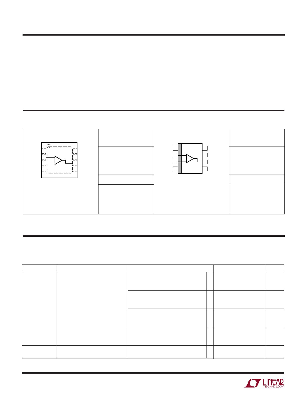
PACKAGE/ORDER I FOR ATIO
TOP VIEW
NULL
1NULL
–IN
2
–
+IN
–
V
8-LEAD (3mm × 3mm) PLASTIC DFN
T
UNDERSIDE METAL INTERNALLY CONNECTED TO V
(PCB CONNECTION OPTIONAL)
*Temperature grades are identified by a label on the shipping container.
Consult LTC Marketing for parts specified with wider operating temperature ranges.
+
3
4
DD PACKAGE
= 125°C, θJA = 160°C/W
JMAX
8
+
V
7
OUT
6
SHDN
5
–
ORDER PART
NUMBER
LT6010CDD
LT6010IDD
LT6010ACDD
LT6010AIDD
DD PART MARKING*
LADU
Maximum Junction Temperature
DD Package ..................................................... 125°C
SO-8 Package .................................................. 150°C
Storage Temperature Range
DD Package ..................................... –65°C to 125°C
SO-8 Package .................................. – 65°C to 150°C
Lead Temperature (Soldering, 10 sec)..................300°C
ORDER PART
NULL
1
–IN
2
+IN
3
–
V
4
8-LEAD PLASTIC SO
T
JMAX
TOP VIEW
8
–
+
S8 PACKAGE
= 150°C, θJA = 190°C/W
7
6
5
NULL
+
V
OUT
SHDN
NUMBER
LT6010CS8
LT6010IS8
LT6010ACS8
LT6010AIS8
S8 PART MARKING
6010
6010I
6010A
6010AI
ELECTRICAL CHARACTERISTICS
The ● denotes the specifications which apply over the full operating
temperature range, otherwise specifications are at TA = 25°C. VS = 5V, 0V; VCM = 2.5V; RL to 0V; SHDN = 0.2V, unless otherwise
specified. (Note 5)
SYMBOL PARAMETER CONDITIONS MIN TYP MAX UNITS
V
OS
∆VOS/∆T Input Offset Voltage Drift (Note 6) LT6010AS8, LT6010S8 ● 0.2 0.8 µV/°C
Input Offset Voltage (Note 7) LT6010AS8 10 35 µV
T
= 0°C to 70°C ● 60 µV
A
= –40°C to 85°C ● 75 µV
T
A
LT6010S8 20 55 µV
= 0°C to 70°C ● 85 µV
T
A
T
= –40°C to 85°C ● 110 µV
A
LT6010ADD 20 60 µV
T
= 0°C to 70°C ● 85 µV
A
= –40°C to 85°C ● 100 µV
T
A
LT6010DD 30 80 µV
= 0°C to 70°C ● 110 µV
T
A
T
= –40°C to 85°C ● 135 µV
A
LT6010ADD,LT6010DD
● 0.2 1.3 µV/°C
sn6010 6010fs
2
LT6010
ELECTRICAL CHARACTERISTICS
The ● denotes the specifications which apply over the full operating
temperature range, otherwise specifications are at TA = 25°C. VS = 5V, 0V; VCM = 2.5V; RL to 0V; SHDN = 0.2V, unless otherwise
specified. (Note 5)
SYMBOL PARAMETER CONDITIONS MIN TYP MAX UNITS
I
OS
I
B
e
n
i
n
R
IN
C
IN
V
CM
CMRR Common Mode Rejection Ratio VCM = 1V to 3.8V ● 107 135 dB
PSRR Power Supply Rejection Ratio VS = 2.7V to 36V, VCM = 1/2V
A
VOL
V
OUT
Input Offset Current (Note 7) LT6010AS8 20 110 pA
= 0°C to 70°C ● 150 pA
T
A
= –40°C to 85°C ● 200 pA
T
A
LT6010S8 40 200 pA
= 0°C to 70°C ● 300 pA
T
A
T
= –40°C to 85°C ● 400 pA
A
LT6010ADD 20 200 pA
= 0°C to 70°C ● 300 pA
T
A
= –40°C to 85°C ● 400 pA
T
A
LT6010DD 40 300 pA
T
= 0°C to 70°C ● 400 pA
A
= –40°C to 85°C ● 500 pA
T
A
Input Bias Current (Note 7) LT6010AS8 20 ±110 pA
= 0°C to 70°C ● ±150 pA
T
A
T
= –40°C to 85°C ● ±200 pA
A
LT6010S8 40 ±200 pA
T
= 0°C to 70°C ● ±300 pA
A
= –40°C to 85°C ● ±400 pA
T
A
LT6010ADD 20 ±200 pA
= 0°C to 70°C ● ±300 pA
T
A
T
= –40°C to 85°C ● ±400 pA
A
LT6010DD 40 ±300 pA
= 0°C to 70°C ● ±400 pA
T
A
= –40°C to 85°C ● ±500 pA
T
A
Input Noise Voltage 0.1Hz to 10Hz 400 nV
P-P
Input Noise Voltage Density f = 1kHz 14 nV/√Hz
Input Noise Current Density f = 1kHz 0.1 pA/√Hz
Input Resistance Common Mode, VCM = 1V to 3.8V 10 120 GΩ
Differential 20 MΩ
Input Capacitance 4pF
Input Voltage Range (Positive) Guaranteed by CMRR ● 3.8 4 V
Input Voltage Range (Negative) Guaranteed by CMRR
● 0.7 1 V
Minimum Supply Voltage Guaranteed by PSRR ● 2.4 2.7 V
S
Large-Signal Voltage Gain RL = 10k, V
R
= 2k, V
L
Maximum Output Swing No Load, 50mV Overdrive 35 55 mV
(Positive, Referred to V
+
) ● 65 mV
I
SOURCE
= 1V to 4V ● 300 2000 V/mV
OUT
= 1V to 4V ● 250 2000 V/mV
OUT
= 1mA, 50mV Overdrive 120 170 mV
● 112 135 dB
● 220 mV
Maximum Output Swing No Load, 50mV Overdrive 40 55 mV
(Negative, Referred to 0V)
I
= 1mA, 50mV Overdrive 150 225 mV
SINK
● 65 mV
● 275 mV
sn6010 6010fs
3
LT6010
ELECTRICAL CHARACTERISTICS
The ● denotes the specifications which apply over the full operating
temperature range, otherwise specifications are at TA = 25°C. VS = 5V, 0V; VCM = 2.5V; RL to 0V; SHDN = 0.2V, unless otherwise
specified. (Note 5)
SYMBOL PARAMETER CONDITIONS MIN TYP MAX UNITS
I
SC
SR Slew Rate AV = –10, RF = 50k, RG = 5k 0.06 0.09 V/µs
GBW Gain Bandwidth Product f = 10kHz 250 330 kHz
t
s
tr, t
f
I
SHDN
t
SHDN
I
S
Output Short-Circuit Current (Note 3) V
Settling Time AV = –1, 0.01%, V
= 0V, 1V Overdrive (Source) 10 14 mA
OUT
V
= 5V, –1V Overdrive (Sink) 10 21 mA
OUT
= 0°C to 70°C ● 0.05 V/µs
T
A
= –40°C to 85°C ● 0.04 V/µs
T
A
= 1.5V to 3.5V 45 µs
OUT
● 4mA
● 4mA
● 225 kHz
Rise Time, Fall Time AV = 1, 10% to 90%, 0.1V Step 1 µs
SHDN Pin Current SHDN ≤ V– + 0.2V (On) ● 0.25 µA
SHDN = V– + 2.0V (Off) ● 15 25 µA
SHDN Turn-On, Turn-Off Time SHDN = V– (On) to V– + 2.0V (Off) 25 µs
SHDN = V
–
+ 2.0V (Off) to V– (On) 25 µs
Supply Current SHDN ≤ V– + 0.2V (On) 135 150 µA
= 0°C to 70°C ● 190 µA
T
A
= –40°C to 85°C ● 210 µA
T
A
SHDN = V– + 2.0V (Off) 12 25 µA
● 50 µA
The ● denotes the specifications which apply over the full operating temperature range, otherwise specifications are at TA = 25°C.
VS = ±15V, VCM = 0V, RL to 0V; SHDN = –14.8V, unless otherwise specified. (Note 5)
SYMBOL PARAMETER CONDITIONS MIN TYP MAX UNITS
V
OS
∆VOS/∆T Input Offset Voltage Drift (Note 6) LT6010AS8, LT6010S8 ● 0.2 0.8 µV/°C
I
OS
Input Offset Voltage (Note 7) LT6010AS8 10 60 µV
= 0°C to 70°C ● 80 µV
T
A
TA = –40°C to 85°C ● 110 µV
LT6010S8 20 85 µV
= 0°C to 70°C ● 120 µV
T
A
= –40°C to 85°C ● 160 µV
T
A
LT6010ADD 20 85 µV
TA = 0°C to 70°C ● 105 µV
= –40°C to 85°C ● 135 µV
T
A
LT6010DD 30 110 µV
= 0°C to 70°C ● 145 µV
T
A
= –40°C to 85°C ● 185 µV
T
A
LT6010ADD,LT6010DD
● 0.2 1.3 µV/°C
Input Offset Current (Note 7) LT6010AS8 20 110 pA
= 0°C to 70°C ● 150 pA
T
A
= –40°C to 85°C ● 200 pA
T
A
LT6010S8 40 200 pA
= 0°C to 70°C ● 300 pA
T
A
= –40°C to 85°C ● 400 pA
T
A
LT6010ADD 20 200 pA
= 0°C to 70°C ● 300 pA
T
A
= –40°C to 85°C ● 400 pA
T
A
sn6010 6010fs
4
LT6010
ELECTRICAL CHARACTERISTICS
The ● denotes the specifications which apply over the full operating
temperature range, otherwise specifications are at TA = 25°C. VS = ±15V, VCM = 0V, RL to 0V; SHDN = –14.8V, unless otherwise
specified. (Note 5)
SYMBOL PARAMETER CONDITIONS MIN TYP MAX UNITS
I
OS
I
B
e
n
i
n
R
IN
C
IN
V
CM
CMRR Common Mode Rejection Ratio VCM = –13.5V to 13.5V 115 135 d B
PSRR Power Supply Rejection Ratio VS = ±1.35V to ±18V ● 112 135 dB
A
VOL
V
OUT
I
SC
Input Offset Current (Note 7) LT6010DD 40 300 pA
= 0°C to 70°C ● 400 pA
T
A
= –40°C to 85°C ● 500 pA
T
A
Input Bias Current (Note 7) LT6010AS8 20 ±110 pA
T
= 0°C to 70°C ● ±150 pA
A
= –40°C to 85°C ● ±200 pA
T
A
LT6010S8 40 ±200 pA
= 0°C to 70°C ● ±300 pA
T
A
T
= –40°C to 85°C ● ±400 pA
A
LT6010ADD 20 ±200 pA
T
= 0°C to 70°C ● ±300 pA
A
= –40°C to 85°C ● ±400 pA
T
A
LT6010DD 40 ±300 pA
= 0°C to 70°C ● ±400 pA
T
A
T
= –40°C to 85°C ● ±500 pA
A
Input Noise Voltage 0.1Hz to 10Hz 400 nV
P-P
Input Noise Voltage Density f = 1kHz 13 nV/√Hz
Input Noise Current Density f = 1kHz 0.1 pA/√Hz
Input Resistance Common Mode, VCM = ±13.5V 50 400 G Ω
Differential 20 MΩ
Input Capacitance 4pF
Input Voltage Range Guaranteed by CMRR ● ±13.5 ±14 V
● 112 dB
Minimum Supply Voltage Guaranteed by PSRR ● ±1.2 ±1.35 V
Large-Signal Voltage Gain RL = 10k, V
RL = 5k, V
Maximum Output Swing No Load, 50mV Overdrive 45 80 mV
(Positive, Referred to V
+
) ● 100 mV
I
SOURCE
= –13.5V to 13.5V 1000 2000 V/mV
OUT
= –13.5V to 13.5V 500 1500 V/mV
OUT
● 600 V/mV
● 300 V/mV
= 1mA, 50mV Overdrive 140 195 mV
● 240 mV
Maximum Output Swing No Load, 50mV Overdrive 45 80 mV
(Negative, Referred to 0V)
Output Short-Circuit Current (Note 3) V
I
= 1mA, 50mV Overdrive 150 250 mV
SINK
= 0V, 1V Overdrive (Source) 10 15 mA
OUT
V
= 0V, –1V Overdrive (Sink) 10 20 mA
OUT
● 100 mV
● 300 mV
● 5mA
● 5mA
sn6010 6010fs
5
LT6010
INPUT COMMON MODE VOLTAGE (V)
–15
120
100
80
60
40
20
0
–20
010
6010 G03
–10 –5
515
OFFSET VOLTAGE (µV)
TA = 85°C
TA = 25°C
TA = –40°C
V
S
= ±15V
TYPICAL PART
ELECTRICAL CHARACTERISTICS
The ● denotes the specifications which apply over the full operating
temperature range, otherwise specifications are at TA = 25°C. VS = ±15V, VCM = 0V, RL to 0V; SHDN = –14.8V, unless otherwise
specified. (Note 5)
SYMBOL PARAMETER CONDITIONS MIN TYP MAX UNITS
SR Slew Rate AV = –10, RF = 50k, RG = 5k 0.08 0.11 V/µs
T
= 0°C to 70°C ● 0.07 V/µs
A
TA = –40°C to 85°C ● 0.05 V/µs
GBW Gain Bandwidth Product f = 10kHz 275 350 kHz
● 250 kHz
t
s
tr, t
f
I
SHDN
t
SHDN
I
S
Note 1: Absolute Maximum Ratings are those beyond which the life of the
device may be impaired.
Note 2: The inputs are protected by back–to–back diodes and internal
series resistors. If the differential input voltage exceeds 10V, the input
current must be limited to less than 10mA.
Note 3: A heat sink may be required to keep the junction temperature
below absolute maximum ratings.
Note 4: Both the LT6010C and LT6010I are guaranteed functional over the
operating temperature range of –40°C to 85°C.
Note 5: The LT6010C is guaranteed to meet the specified performance
Settling Time AV = –1, 0.01%, V
= 0V to 10V 85 µs
OUT
Rise Time, Fall Time AV = 1, 10% to 90%, 0.1V Step 1 µs
SHDN Pin Current SHDN ≤ V– + 0.2V (On) ● 0.25 µA
SHDN = V– + 2.0V (Off) ● 15 25 µA
SHDN Turn-On, Turn-Off Time SHDN = V– (On) to V– + 2.0V (Off) 25 µs
SHDN = V
–
+ 2.0V (Off) to V– (On) 25 µs
Supply Current SHDN ≤ V– + 0.2V (On) 260 330 µA
T
= 0°C to 70°C ● 380 µA
A
TA = –40°C to 85°C ● 400 µA
SHDN = V– + 2.0V (Off) 18 50 µA
from 0°C to 70°C and is designed, characterized and expected to meet
specified performance from –40°C to 85°C but is not tested or QA
sampled at these temperatures. The LT6010I is guaranteed to meet
specified performance from –40°C to 85°C.
Note 6: This parameter is not 100% tested.
Note 7: The specifications for V
, IB and IOS depend on the grade and on
OS
the package. The following table clarifies the notations used in the
specification table:
Standard Grade A Grade
S8 Package LT6010S8 LT6010AS8
DFN Package LT6010DD LT6010ADD
UW
TYPICAL PERFOR A CE CHARACTERISTICS
Input Offset Voltage
Distribution of Input Offset Voltage
30
VS = 5V, 0V
= 25°C
T
A
25
20
15
10
PERCENT OF UNITS (%)
6
5
0
–45 –35 –15 –5 5 15 25 35 45
–25
INPUT OFFSET VOLTAGE (µV)
LT6010AS8
6010 G01
vs Temperature
125
VS = 5V, 0V
100
REPRESENTATIVE UNITS
75
50
25
0
–25
–50
OFFSET VOLTAGE (µV)
–75
–100
–125
–50
–25
25
0
TEMPERATURE (°C)
Offset Voltage
vs Input Common Mode Voltage
50
75
100
125
6010 G02
sn6010 6010fs
UW
LOAD CURRENT (mA)
0.01
0.01
OUTPUT LOW SATURATION VOLTAGE (V)
0.1
1
0.1 1 10
6010 G12
TA = 85°C
TA = 25°C
VS = 5V, 0V
TA = –40°C
FREQUENCY (Hz)
1
10
INPUT VOLTAGE NOISE DENSITY (nV/√Hz)
INPUT CURRENT NOISE DENSITY (fA/√Hz)
100 100
1000
10 100 1000
6010 G06
CURRENT NOISE
VOLTAGE NOISE
VS = ±15V
T
A
= 25°C
TYPICAL PERFOR A CE CHARACTERISTICS
Input Bias Current
Input Bias Current vs Temperature
1000
VS = 5V, 0V
900
TYPICAL PART
800
700
600
500
400
300
200
INPUT BIAS CURRENT (pA)
100
–100
0
–50
+
I
B
–
I
B
0
–25
TEMPERATURE (°C)
25
50
Total Input Noise
vs Source Resistance
10
VS = 5V, 0V
= 25°C
T
A
f = 1kHz
1
75 100
125
6010 G04
vs Input Common Mode Voltage
100
TA = –40°C
20pA/DIV
–100
–15
TA = 85°C
TA = 25°C
2V/DIV
0.1Hz to 10Hz Noise
VS = ±15V
= 25°C
T
A
6010 G05
LT6010
en, in vs Frequency
15
0.01Hz to 1Hz Noise
VS = ±15V
T
= 25°C
A
0.1
TOTAL NOISE
0.01
RESISTOR NOISE ONLY
0.001
TOTAL INPUT NOISE (µV/√Hz)
0.0001
100 1k 10k 100k 1M 10M
SOURCE RESISTANCE (Ω)
Output Voltage Swing
vs Temperature
+
V
–20
–40
–60
60
40
OUTPUT VOLTAGE SWING (mV)
20
–
V
–25 0 50
–50
TEMPERATURE (°C)
OUTPUT HIGH
OUTPUT LOW
25
75 100 125
6010 G07
VS = 5V, 0V
NO LOAD
6010 G10
100M
NOISE VOLTAGE (0.2µV/DIV)
246 107135 9
0
TIME (SEC)
Output Saturation Voltage
vs Load Current (Output High)
1
VS = 5V, 0V
TA = 85°C
TA = 25°C
0.1
TA = –40°C
OUTPUT HIGH SATURATION VOLTAGE (V)
0.01
0.01
0.1 1 10
LOAD CURRENT (mA)
NOISE VOLTAGE (0.2µV/DIV)
8
6010 G08
20 40 60 1007010 30 50 90
0
TIME (SEC)
80
6010 G09
Output Saturation Voltage
vs Load Current (Output Low)
6010 G11
sn6010 6010fs
7

LT6010
SETTLING TIME (µs)
0
0
OUTPUT STEP (V)
2
6
8
10
20
40
50 90
6010 G18
4
10 30
60
70
80
VS = ±15V
A
V
= –1
0.1%
0.01%
UW
TYPICAL PERFOR A CE CHARACTERISTICS
Supply Current vs Supply Voltage
500
450
400
350
300
250
200
150
SUPPLY CURRENT (µA)
100
50
0
0
TA = 25°C
42
SUPPLY VOLTAGE (±V)
86
10
TA = 85°C
TA = –40°C
12 14 18
16
20
6010 G13
Warm-Up Drift THD + Noise vs Frequency
3
2
1
CHANGE IN OFFSET VOLTAGE (µV)
0
30 60 90 120
TIME AFTER POWER-ON (SECONDS)
±15V
±2.5V
150
6010 G14
10
VS = 5V, 0V
V
OUT
TA = 25°C
1
= 1: RL = 10k
A
V
= –1: RF = RG = 10k
A
V
0.1
0.01
THD + NOISE (%)
0.001
0.0001
10
= 2V
P-P
AV = –1
1k 10k100 100k
FREQUENCY (Hz)
THD + Noise vs Frequency Settling Time vs Output Step Settling Time vs Output Step
10
VS = ±15V
= 20V
V
IN
TA = 25°C
1
0.1
0.01
THD + NOISE (%)
0.001
P-P
AV = –1
AV = 1
10
VS = ±15V
= 1
A
V
8
6
4
OUTPUT STEP (V)
2
0.1%
0.01%
AV = 1
6010 G15
0.0001
0
10 30
20
10
FREQUENCY (Hz)
1k 10k100
6010 G16
0
40
SETTLING TIME (µs)
CMRR vs Frequency
160
TA = 25°C
140
120
100
VS = ±15V
6010 G20
80
60
40
20
COMMON MODE REJECTION RATIO (dB)
0
110
100 1k 10k 100k 1M
FREQUENCY (Hz)
VS = 5V, 0V
70
50 90
80
60
6010 G17
PSRR vs Frequency
140
120
100
80
60
40
20
POWER SUPPLY REJECTION RATIO (dB)
0
1 10 100 1k 10k 100k 1M
0.1
+PSRR
–PSRR
FREQUENCY (Hz)
VS = 5V, 0V
= 25°C
T
A
6010 G21
sn6010 6010fs
8
UW
TYPICAL PERFOR A CE CHARACTERISTICS
Output Impedance vs Frequency Open-Loop Gain vs Frequency Gain and Phase vs Frequency
1000
VS = 5V, 0V
= 25°C
T
A
100
10
AV = 100
1
AV = 10
OUTPUT IMPEDANCE (Ω)
0.1
AV = 1
0.01
1 100 1k 10k 100k 1M
10
FREQUENCY (Hz)
6010 G22
140
120
100
80
60
40
20
OPEN-LOOP GAIN (dB)
0
–20
–40
0.1 1
0.01 10 100 1k 10k 100k 1M 10M
FREQUENCY (Hz)
VS = 5V, 0V
T
A
R
L
= 25°C
= 10k
6010 G23
60
50
40
30
20
10
0
–10
OPEN-LOOP GAIN (dB)
–20
–30
–40
1k 100k 1M 10M
GAIN
10k
FREQUENCY (Hz)
LT6010
VS = 5V, 0V
= 25°C
T
A
= 10k
R
L
PHASE
–80
–120
PHASE SHIFT (DEG)
–160
–200
–240
–280
6010 G24
Gain vs Frequency, AV = 1 Gain vs Frequency, AV = –1
10
5
0
–5
GAIN (dB)
–10
–15
–20
1k
VS = 5V, 0V
= 25°C
T
A
CL = 500pF
CL = 50pF
10k 100k 1M
FREQUENCY (Hz)
6010 G25
10
5
0
–5
GAIN (dB)
–10
–15
–20
1k
VS = 5V, 0V
= 25°C
T
A
10k 100k 1M
FREQUENCY (Hz)
CL = 500pF
CL = 50pF
6010 G26
vs Temperature
40
35
30
25
20
15
VS = 5V, 0V
10
5
SUPPLY CURRENT IN SHUTDOWN (µA)
0
–20–30 0 30 40 60 70 9020 50
–40
Small-Signal Transient Response Large-Signal Transient Response Rail-to-Rail Output Swing
1V/DIV
Supply Current in Shutdown Mode
20mV/DIV
2V/DIV
0V
VS = ±15V
10–10
TEMPERATURE (°C)
80
6010 G30
5V
= 1 2µs/DIV 6011 G27
A
V
= –1 50µs/DIV 6011 G28
A
V
VS = ±15V
= –1 100µs/DIV 6011 G29
A
V
VS = 5V, 0V
sn6010 6010fs
0V
9

LT6010
WUUU
APPLICATIO S I FOR ATIO
Preserving Input Precision
Preserving the input accuracy of the LT6010 requires that
the applications circuit and PC board layout do not introduce errors comparable to or greater than the 20µV typical
offset of the amplifier. Temperature differentials across
the input connections can generate thermocouple voltages of 10’s of microvolts, so the connections to the input
leads should be short, close together, and away from heat
dissipating components. Air currents across the board
can also generate temperature differentials.
The extremely low input bias currents (20pA typical) allow
high accuracy to be maintained with high impedance
sources and feedback resistors. The LT6010 low input
bias currents are obtained by a cancellation circuit onchip. The input bias currents are permanently trimmed at
wafer testing to a low level. Do not try to balance the input
resistances in each input lead; instead, keep the resistance
at either input as low as possible for maximum accuracy.
Leakage currents on the PC board can be higher than the
LT6010’s input bias current. For example, 10GΩ of leakage between a 15V supply lead and an input lead will generate 1.5nA! Surround the input leads by a guard ring, driven
to the same potential as the input common mode, to avoid
excessive leakage in high impedance applications.
allowed) for a 10V differential input voltage. Use additional
external series resistors to limit the input current to 10mA
in applications where differential inputs of more than 10V
are expected. For example, a 1k resistor in series with each
input provides protection against 30V differential voltage.
Input Common Mode Range
The LT6010 output is able to swing nearly to each power
supply rail (rail-to-rail out), but the input stage is limited to
operating between V– + 1V and V+ – 1.2V. Exceeding this
common mode range will cause the gain to drop to zero,
however no phase reversal will occur.
Total Input Noise
The LT6010 amplifier contributes negligible noise to the
system when driven by sensors (sources) with impedance
between 20kΩ and 1MΩ. Throughout this range, total
input noise is dominated by the 4kTRS noise of the source.
If the source impedance is less than 20kΩ, the input
voltage noise of the amplifier starts to contribute with a
minimum noise of 14nV/√Hz for very low source impedance. If the source impedance is more than 1MΩ, the input
current noise of the amplifier, multiplied by this high
impedance, starts to contribute and eventually dominate.
Total input noise spectral density can be calculated as:
Input Protection
The LT6010 features on-chip back-to-back diodes between the input devices, along with 500Ω resistors in
series with either input. This internal protection limits the
input current to approximately 10mA (the maximum
10
v e kTR i R
n TOTAL n S n S()
where en = 14nV/√Hz, in = 0.1pA/√Hz and RS the total
impedance at the input, including the source impedance.
2
4
()=+ +
2
sn6010 6010fs

WUUU
APPLICATIO S I FOR ATIO
LT6010
Offset Voltage Adjustment
The input offset voltage of the LT6010 and its drift with
temperature are permanently trimmed at wafer testing to
the low level as specified in the electrical characteristic.
However, if further adjustment of V
is desired, nulling with
OS
a 50k potentiometer is possible and will not degrade drift
with temperature. Trimming to a value other than zero
Standard Adjustment
7
6
6010 F01a
V
CC
50k
1
8
2
–
LT6010INPUT OUTPUT
3
+
4
V
ee
Figure 1A Figure 1B
creates a drift of (VOS/300µV) µV/°C, e.g., if VOS is adjusted
to 300µV, the change in drift will be 1µV/°C. The adjustment
range with a 50k pot is approximately ±0.9mV (see Figures
1A and 1B). The sensitivity and resolution of the nulling can
be improved by using a smaller pot in conjunction with fixed
resistors. The configuration shown has an approximate
nulling range of ±150µV (see Figures 2A and 2B).
1.0
0.8
0.6
0.4
0.2
0
–0.2
–0.4
–0.6
CHANGE IN OFFSET VOLTAGE (mV)
–0.8
–1.0
0 0.2 0.4 0.6 0.8 1.0
POTENTIOMETER POSITION
6010 F01b
10k
V
50k
10k
1
8
2
–
INPUT OUTPUT
LT6010
3
+
4
V
ee
CC
7
6
6010 F02a
Figure 2A Figure 2B
Improved Sensitivity Adjustment
200
150
100
50
0
–50
–100
CHANGE IN OFFSET VOLTAGE (µV)
–150
–200
0.2 0.4 0.6 0.8
0
POTENTIOMETER POSITION
1.0
6010 F02b
sn6010 6010fs
11
LT6010
R
G
V
REF
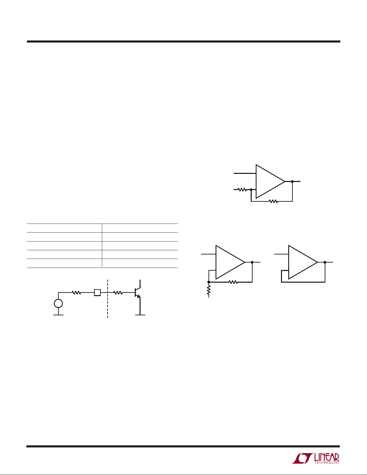
NONINVERTING: AV = 1 + RF/R
G
INPUTS MOVE AS MUCH AS
V
IN
, BUT THE OUTPUT MOVES
MORE
INPUT MAY NOT HAVE TO BE
RAIL-TO-RAIL
NONINVERTING: A
V
= 1
INPUTS MOVE AS MUCH AS THE
OUTPUT
INPUT MUST BE RAIL-TO-RAIL
FOR OVERALL CIRCUIT
RAIL-TO-RAIL PERFORMANCE
INVERTING: A
V
= –RF/R
G
OP AMP INPUTS DO NOT MOVE,
BUT ARE FIXED AT DC BIAS
POINT V
REF
INPUT DOES NOT HAVE TO BE
RAIL-TO-RAIL
V
IN
R
F
–
+
V
IN
V
REF
R
F
R
G
–
+
V
IN
6010 F04
–
+
WUUU
APPLICATIO S I FOR ATIO
Shutdown
The LT6010 can be put into shutdown mode to conserve
power. When the SHDN pin is biased at less than 0.2V
above the negative supply, the part operates normally.
When pulled 2V or more above V–, the supply current
drops to about 12µA, shutting down the op amp.
The output of the LT6010 op amp is not isolated from the
inputs while in shutdown mode. Therefore, this shutdown
feature cannot be used for multiplexing applications.
There is an internal 85k resistor at the SHDN pin. If the
SHDN voltage source is more than 2V above the negative
supply, an external series resistor can be placed between
the source and SHDN pin to reduce SHDN pin current (see
Figure 3). For an example of suggested values see Table 1.
The resistors listed ensure that the voltage at the SHDN pin
is 2V above the negative supply.
Table 1
V
(V) R
SHDN
2 NONE
3 77k
4 153k
5 230k
SHDN
(kΩ)
Rail-to-Rail Operation
The LT6010 outputs can swing to within millivolts of either
supply rail, but the inputs cannot. However, for most op
amp configurations, the inputs need to swing less than the
outputs. Figure 4 shows the basic op amp configurations,
lists what happens to the op amp inputs and specifies
whether or not the op amp must have rail-to-rail inputs.
Select a rail-to-rail input op amp only when really necessary, because the input precision specifications are usually inferior.
Capacitive Loads
The LT6010 can drive capacitive loads up to 500pF in unity
gain. The capacitive load driving capability increases as
the amplifier is used in higher gain configurations. A small
series resistance between the output and the load further
increases the amount of capacitance that the amplifier can
drive.
12
R
SHDN
SHDN
+
V
SHDN
–
V
EE
Figure 3
5
85k
V
6010 F03
EE
Figure 4. Some Op Amp Configurations Do Not Require
Rail-to-Rail Inputs to Achieve Rail-to-Rail Outputs
sn6010 6010fs
WW
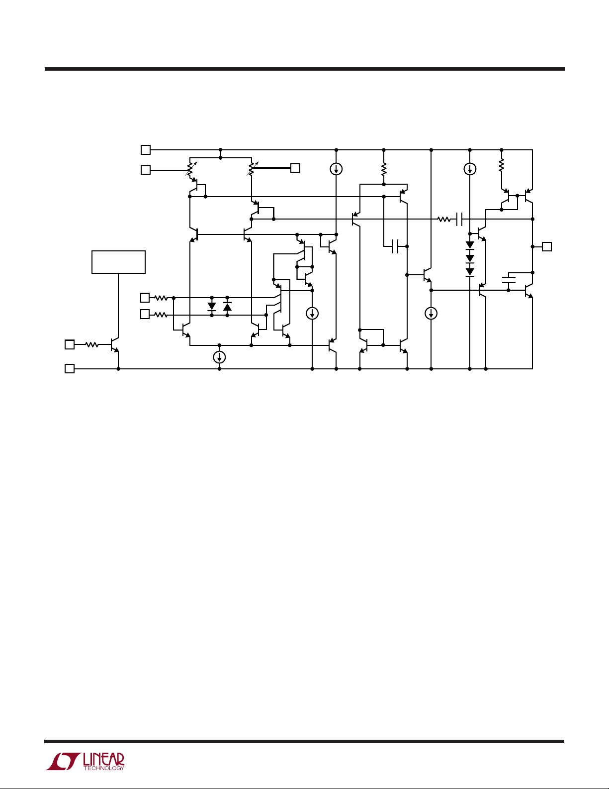
SI PLIFIED SCHE ATIC
+
7
V
R3 R4
Q7
Q8
Q3
D2D1
Q1 Q2
SHDN
1
NULL
BIAS CURRENT
GENERATOR
R1
500Ω
2
–IN
3
+IN
R2
500Ω
5
LT6010
Q13
Q14
Q18
R6
Q19
OUT
6
C3
Q20
8
NULL
Q4
Q10
Q21
B
A
C
B
A
Q11
Q16
Q17
Q15
Q9
R5
Q6
C1
R
Q12
C1
D3
D4
D5
Q5
C2
Q10
–
4
V
6010 SS
sn6010 6010fs
13

LT6010
PACKAGE DESCRIPTIO
U
DD Package
8-Lead Plastic DFN (3mm × 3mm)
(Reference LTC DWG # 05-08-1698)
0.675 ±0.05
3.5 ±0.05
1.65 ±0.05
(2 SIDES)2.15 ±0.05
PACKAGE
OUTLINE
0.28 ± 0.05
RECOMMENDED SOLDER PAD PITCH AND DIMENSIONS
PIN 1
TOP MARK
0.200 REF
NOTE:
1. DRAWING TO BE MADE A JEDEC PACKAGE OUTLINE M0-229 VARIATION OF (WEED-1)
2. ALL DIMENSIONS ARE IN MILLIMETERS
3. DIMENSIONS OF EXPOSED PAD ON BOTTOM OF PACKAGE DO NOT INCLUDE
MOLD FLASH. MOLD FLASH, IF PRESENT, SHALL NOT EXCEED 0.15mm ON ANY SIDE
4. EXPOSED PAD SHALL BE SOLDER PLATED
0.50
BSC
2.38 ±0.05
(2 SIDES)
3.00 ±0.10
(4 SIDES)
0.75 ±0.05
0.00 – 0.05
1.65 ± 0.10
(2 SIDES)
R = 0.115
TYP
0.28 ± 0.05
2.38 ±0.10
(2 SIDES)
BOTTOM VIEW—EXPOSED PAD
0.38 ± 0.10
85
14
0.50 BSC
(DD8) DFN 0203
14
sn6010 6010fs

PACKAGE DESCRIPTIO
.050 BSC
U
S8 Package
8-Lead Plastic Small Outline (Narrow .150 Inch)
(Reference LTC DWG # 05-08-1610)
.189 – .197
.045 ±.005
(4.801 – 5.004)
8
NOTE 3
7
6
LT6010
5
.245
MIN
.030 ±.005
TYP
RECOMMENDED SOLDER PAD LAYOUT
.010 – .020
(0.254 – 0.508)
.008 – .010
(0.203 – 0.254)
NOTE:
1. DIMENSIONS IN
2. DRAWING NOT TO SCALE
3. THESE DIMENSIONS DO NOT INCLUDE MOLD FLASH OR PROTRUSIONS.
MOLD FLASH OR PROTRUSIONS SHALL NOT EXCEED .006" (0.15mm)
× 45°
.016 – .050
(0.406 – 1.270)
INCHES
(MILLIMETERS)
.160
±.005
.228 – .244
(5.791 – 6.197)
0°– 8° TYP
.053 – .069
(1.346 – 1.752)
.014 – .019
(0.355 – 0.483)
TYP
.150 – .157
(3.810 – 3.988)
NOTE 3
1
3
2
4
.004 – .010
(0.101 – 0.254)
.050
(1.270)
BSC
SO8 0303
Information furnished by Linear Technology Corporation is believed to be accurate and reliable.
However, no responsibility is assumed for its use. Linear Technology Corporation makes no representation that the interconnection of its circuits as described herein will not infringe on existing patent rights.
sn6010 6010fs
15

LT6010
TYPICAL APPLICATIO
U
Precision JFET Input Transimpedance Photodiode Amplifier
C4
0.5pF
+
V
J1
+
U1
LT6010
R1
330k, 5%
S1
–
V
–
C2
0.1µF
0.01µF
R2
1k
5%
C1
R4
2.55k
–
V
C3
1pF
R3
100k, 1%
–
U2
LT6230
V
OUT
+
J1: PHILIPS BF862
S1: SIEMENS/INFINEON SFH203 PHOTODIODE (~3pF)
= ±5V
V
SUPPLY
I
= 5.6mA
SUPPLY
BANDWIDTH = 6MHz
A
= 100kΩ
Z
OUTPUT OFFSET ≈ 50µV TYPICALLY
RELATED PARTS
PART NUMBER DESCRIPTION COMMENTS
LT6011/6012 Dual/Quad Precision Op Amps 135µA, Rail-to-Rail Output
LT1001 Low Power, Picoamp Input Precision Op Amp 250pA Input Bias Current
LT1880 Rail-to-Rail Output, Picoamp Input Precision Op Amp C
up to 1000pF
LOAD
6010 TA02
16
Linear Technology Corporation
1630 McCarthy Blvd., Milpitas, CA 95035-7417
(408) 432-1900 ● FAX: (408) 434-0507
●
www.linear.com
sn6010 6010fs
LT/TP 1203 1K • PRINTED IN USA
LINEAR TECHNOLOGY CORPORATION 2003
 Loading...