

Page 1
Fast Time Division Duplex (TDD) Transmission Using an
Upconverting Mixer with a High Side Switch –
Design Note 480
Vladimir Dvorkin
Introduction
Many wireless infrastructure time division duplex (TDD)
transmit applications require fast on/off switching of the
transmitter, typically within one to fi ve microseconds.
There are several different ways to implement fast Tx
on/off switching, including the use of RF switches in the
signal path, or on/off switching of the supply voltage for
different stages of the transmitter chain. The advantages
of the latter method are low cost, very good performance
and power saving during the Tx off-time. In particular, a
good place to apply supply switching is at the transmit
upconverting mixer because this removes both the
transmit signal and all other mixing products from the
mixer RF output.
®
The LT
various TDD and Burst Mode
5579 high performance upconverting mixer fi ts
®
transmitter applications
with out put freque ncies up to 3.8 GHz . Fast o n/of f supply
voltage (V
) switching for the LT5579 is as simple as
CC
adding an external high side power supply switch (note
that this technique is equally effective for the lower frequency upconverting mixer, LT5578).
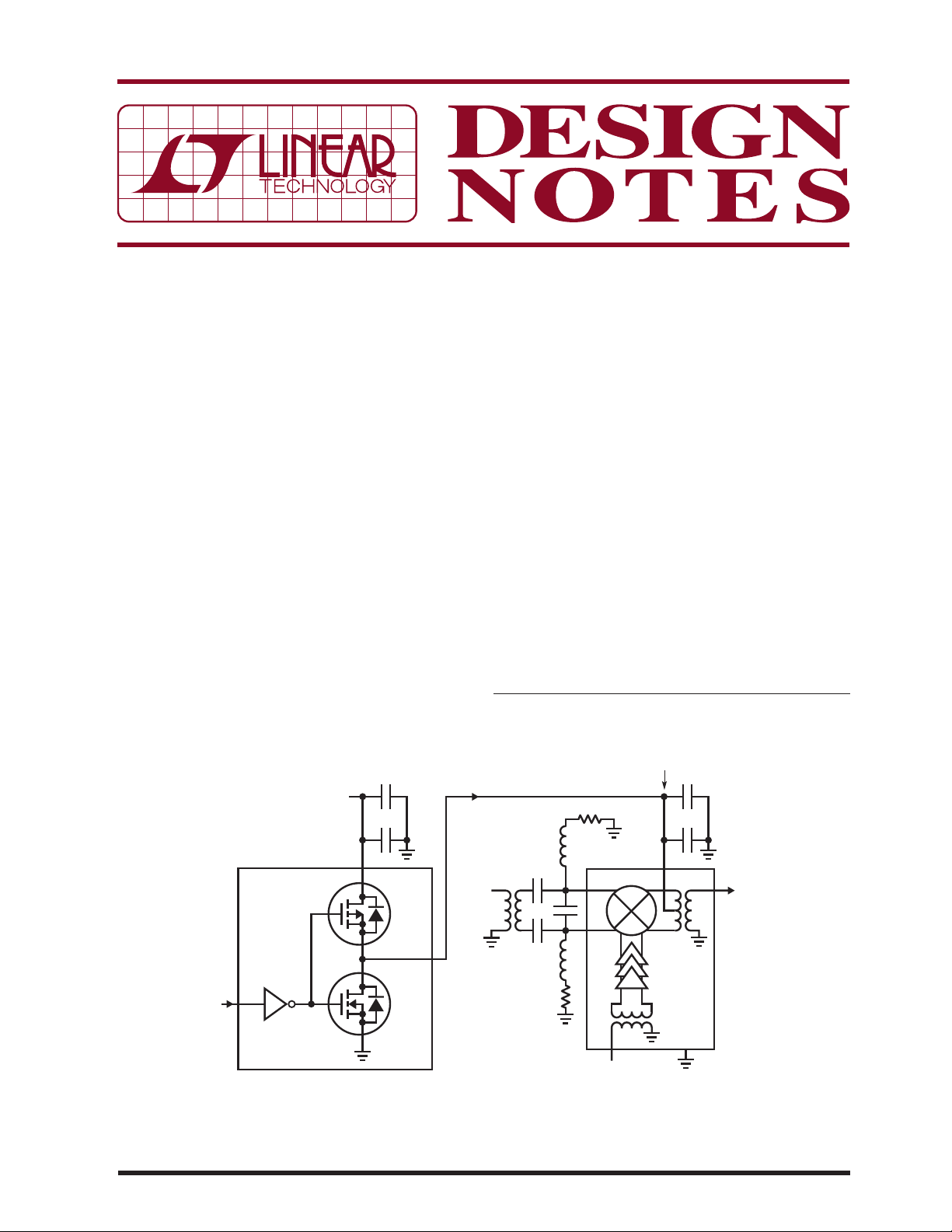
High Side VCC Switch for a Burst Mode Transmitter
Using the LT5579 Mixer
The high side VCC s w i t c h c i r c ui t i n F ig u r e 1 u s e s a P - c h a n nel MOSFET (IRLML6401) with an R
0.1Ω. An N-channel enhancement mode FET (2N7002),
connected fr om the drain of IRLML6401 to ground, fur ther
improves fall time. The 2N7002’s R
which is suffi cient for this application.
The input driver for the high side V
speed CMOS inverter (MC74HC1G04) capable of driving
capacitive loads. The IRLML6401 input capacitance is
typically 830pF and the 2N7002 input capacitance is
L, LT, LTC, LTM, Burst Mode, Linear Technology and the Linear logo are registered
trademarks of Linear Technology Corporation. All other trademarks are the property of
their respective owners.
of less than
DS(ON)
i s le s s t ha n 4 Ω ,
DS(ON)
switch is a high
CC
07/10/480
V
ON/OFF
CONTROL
CC
HIGH SIDE
SWITCH
V
CC
IRLML6401
MC74HC1G04
V
CC
= 3.3V
G
G
1.0μF
33pF
S
240MHz
D
D
2N7002
S
Tx IF
INPUT
4:1
Tr- r
39nH
33pF
33pF
39nH
11Ω
ON STATE V
11Ω
IF
IF
LO INPUT
+
–
LO
Figure 1. Upconverting Mixer with High Side VCC Switch
= 3.29V
CC
+
270pF
33pF
V
CC
RF
RF OUTPUT
2140MHz
LT5579
–
LO
GND
DN4VD F01
Page 2
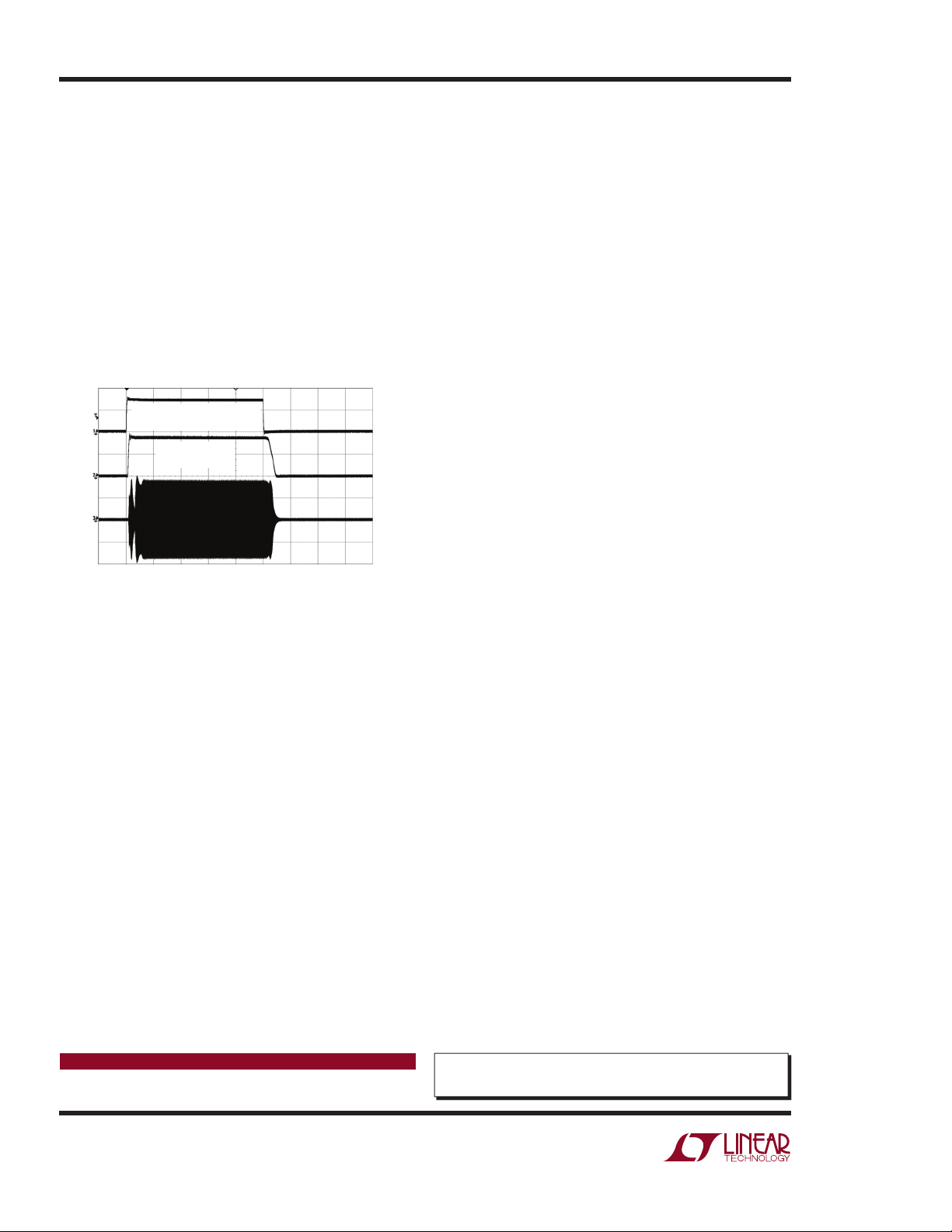
under 50pF. For faster rise times, two high speed CMOS
drivers can be used in parallel. Likewise, for faster fall
times, a different N-channel MOSFET with lower on-resistance can be used.
With the LT5579 supply current of 220mA, the power
supply voltage drop across the MOSFET is only 11mV.
The response time of the high side V
switch is shown
CC
in Figure 2. Total turn-on time is only 650ns and total
turn-off time is 500ns. These measurements were performed using two RF bypass capacitors at the mixer V
CC
pin (33pF and 270pF). Higher value RF bypass capacitors can be used, which would result in correspondingly
slower rise/fall times.
INPUT CONTROL SIGNAL
FOR HIGH SIDE V
HIGH SIDE V
SWITCH OUTPUT
LT5579 RF OUTPUT
Figure 2. VCC Turn-On and Turn-Off Waveforms
SWITCH
CC
CC
1μs/DIV
DN4VD F02
The LT5579 upconverting mixer circuit shown in Figure 1
was optimized and tested at an RF output frequency of
2140MHz. The RF output envelope in Figure 2 shows a dip
about 300ns after the V
switch turns on, followed by
CC
another, smaller dip at about the 500ns point. Both dips
represent the mixer’s internal feedback circuit reaction
to the ramping supply voltage.
LO leakage to the RF output of the LT5579 was measured
at –40dBm when V
LO port of the LT5579 is internally matched and has a
is on and –46dBm for VCC off. The
CC
return loss of 10dB to 18dB over a frequency range of
1100MHz to 3200MHz.
When the LT5579 mixer is in the off state, the return
loss of the LO port is about 3dB to 5dB across the same
frequency range of 1100MHz to 3200MHz. It is advisable
to use an LO injection VCO with a buffered output for
better reverse isolation, and to avoid any VCO pulling
while the LO port impedance changes when switching
between the on and off states.
Conclusion
LT5579 and LT5578 mixers without an ENABLE pin can
be used in TDD applications with external V
switch-
CC
ing. Using only three parts (IRLML6401, 2N7002 and an
MC74HC1G04), a high performance high side V
switch
CC
allows turn-on and turn-off in under 1μs.
Data Sheet Download
www.linear.com
Linear Technology Corporation
1630 McCarthy Blvd., Milpitas, CA 95035-7417
(408) 432-1900
●
FAX: (408) 434-0507 ● www.linear.com
For applications help,
call (408) 432-1900, Ext. 3866
dn480f LT/TP 0710 116K • PRINTED IN THE USA
© LINEAR TECHNOLOGY CORPORATION 2010
 Loading...