

FEATURES
■
RF Frequency Range: 50MHz to 3GHz
■
Linear Dynamic Range: 60dB
■
Exceptional Accuracy over Temperature
and Power Supply
■
Fast Transient Response:
38ns Full-Scale Settling Time
■
Single 2.7V to 5.25V Supply
■
Low Supply Current: 7mA
■
Shutdown Current: 0.1µA
■
Tiny 6-Lead SC70 Package
U
APPLICATIO S
■
RF RSSI and ACC
■
RF Power Control
■
CATV Power Detection
■
Optical Receiver Gain Control
LT5534
50MHz to 3GHz
RF Power Detector
with 60dB Dynamic Range
U
DESCRIPTIO
The LT®5534 is a 50MHz to 3GHz monolithic RF power
detector capable of measuring RF signals over a 60dB
dynamic range. The RF signal in a decibel scale is precisely
converted into DC voltage on a linear scale. The 60dB input
dynamic range is achieved using cascaded RF detectors
and RF limiters. Their outputs are summed to generate an
accurate log-linear DC voltage proportional to the input RF
signal in dB. The output is buffered with a low output
impedance driver. The LT5534 delivers superior temperature stability (typical output variation within ±1dB over the
full temperature range). The output responds in less than
40ns to a large RF input signal.
, LTC and LT are registered trademarks of Linear Technology Corporation.
All other trademarks are the property of their respective owners.
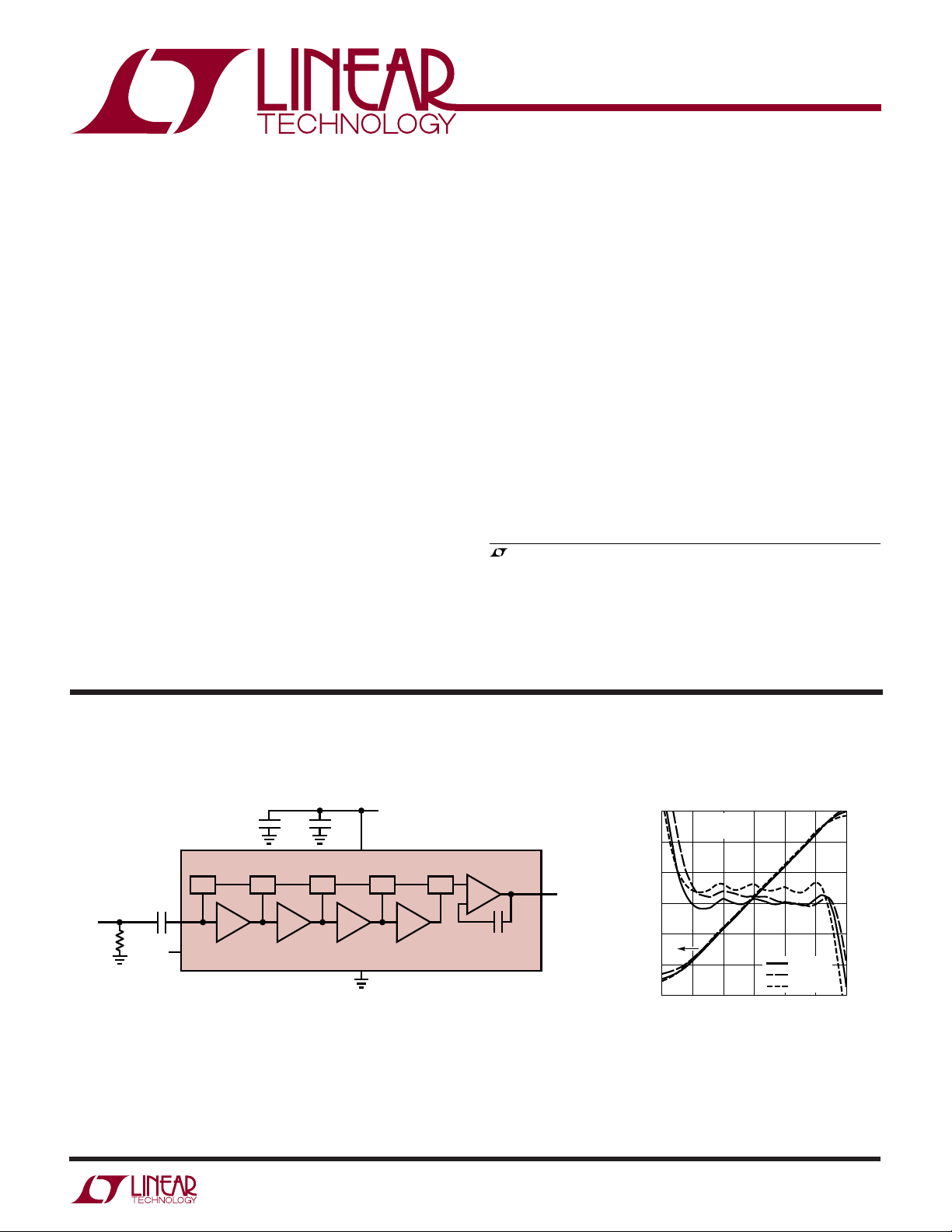
TYPICAL APPLICATIO
50MHz to 3GHz RF Power Detector
0.1µF
LT5534
1nF
INPUT
RF
47Ω
ENABLE
RF
EN
U
100pF
V
GND
Output Voltage
vs RF Input Power
3V
CC
DETDETDETDETDET
V
OUT
5534 TA01
V
OUT
(V)
V
OUT
2.4
2.0
1.6
1.2
0.8
0.4
0
–60
VCC = 3V
AT 900MHz
–40 –30 –20
–50
RF INPUT POWER (dBm)
TA = 25°C
= 85°C
T
A
A = –40C
T
–10 0
5534 G05
3
2
LINEARITY ERROR (dB)
1
0
–1
–2
–3
5534fa
1
LT5534
WW
W
ABSOLUTE MAXIMUM RATINGS
(Note 1)
Power Supply Voltage ............................................ 5.5V
Enable Voltage ....................................................0V, V
RF Voltage (+10dBm Equivalent) ............................. ±1V
Operating Ambient Temperature Range .. –40°C to 85°C
Storage Temperature Range ................. –65°C to 125°C
Lead Temperature (Soldering, 10 sec).................. 300°C
ELECTRICAL CHARACTERISTICS
noted. Test circuit shown in Figure 1. (Note 2)
PARAMETER CONDITIONS MIN TYP MAX UNITS
RF Input
Frequency Range 50 to 3000 MHz
Input Impedance 2kΩ
fRF = 50MHz
RF Input Power Range –58 to +2 dBm
Dynamic Range (Note 3) ±3dB Linearity Error, TA = –40°C to 85°C60dB
Output Slope 44 mV/dB
Output Variation vs Temperature PIN = –48dBm to –14dBm, TA = –40°C to 85°C 0.007 dB/°C
fRF = 900MHz
RF Input Power Range –60 to 0 dBm
Dynamic Range (Note 3) ±3dB Linearity Error, TA = –40°C to 85°C60dB
Output Slope 41 mV/dB
Output Variation vs Temperature PIN = –48dBm to –14dBm, TA = –40°C to 85°C 0.008 dB/°C
fRF = 1900MHz
RF Input Power Range –63 to –2 dBm
Dynamic Range (Note 3) ±3dB Linearity Error, TA = –40°C to 85°C61dB
Output Slope 31 36.6 43 mV/dB
Output Variation vs Temperature PIN = –48dBm to –14dBm, TA = –40°C to 85°C 0.012 dB/°C
Output Intercept 50Ω External Termination, TA = –40°C to 85°C –70 –64 –58 dBm
fRF = 2500MHz
RF Input Power Range –63 to –3 dBm
Dynamic Range (Note 3) ±3dB Linearity Error, TA = –40°C to 85°C60dB
Output Slope 35 mV/dB
Output Variation vs Temperature PIN = –48dBm to –14dBm, TA = –40°C to 85°C 0.025 dB/°C
Output Interface
Output DC Voltage No RF Input Signal 30 142 240 mV
Output Impedance 32 Ω
Output Bandwidth 30 MHz
Full-Scale Setting Time Input from No Signal to –2dBm, to 90% 38 ns
Sinking/Sourcing 10/200 mA/µA
U
U
W
PACKAGE/ORDER INFORMATION
TOP VIEW
CC
Order Options Tape and Reel: Add #TR
Lead Free: Add #PBF Lead Free Tape and Reel: Add #TRPBF
Lead Free Part Marking: http://www.linear.com/leadfree/
Consult LTC Marketing for parts specified with wider operating temperature ranges.
VCC = 3V, EN = 3V, TA = 25°C, source impedance = 50Ω, unless otherwise
EN 1
GND 2
V
3
OUT
SC6 PACKAGE
6-LEAD PLASTIC SC70
T
= 125°C, θJA = 256°C/W
JMAX
6 RF
5 GND
4 V
CC
ORDER PART
NUMBER
LT5534ESC6
SC6 PART
MARKING
LBGD
U
5534fa
2
LT5534
ELECTRICAL CHARACTERISTICS
VCC = 3V, EN = 3V, TA = 25°C, unless otherwise noted.
Test circuit shown in Figure 1. (Note 2)
PARAMETER CONDITIONS MIN TYP MAX UNITS
Power Up/Down
Turn-On Time 200 ns
Turn-Off Time 800 ns
EN = High (On) 0.9 V
EN = Low (Off) 0.6 V
Power Supply
Supply Voltage 2.7 5.25 V
Supply Current EN = High 5 7 9 mA
Shutdown Current EN = Low 0.1 10 µA
Note 1: Absolute Maximum Ratings are those values beyond which the life
of a device may be impaired.
Note 2: Specifications over the –40°C to 85°C temperature range are
assured by design, characterization and correlation with statistical process
Note 3: The linearity error is calculated by the difference between the
incremental slope of the output and the average output slope from
–48dBm to –14dBm. The dynamic range is defined as the range over
which the linearity error is within ±3dB.
control.
UW
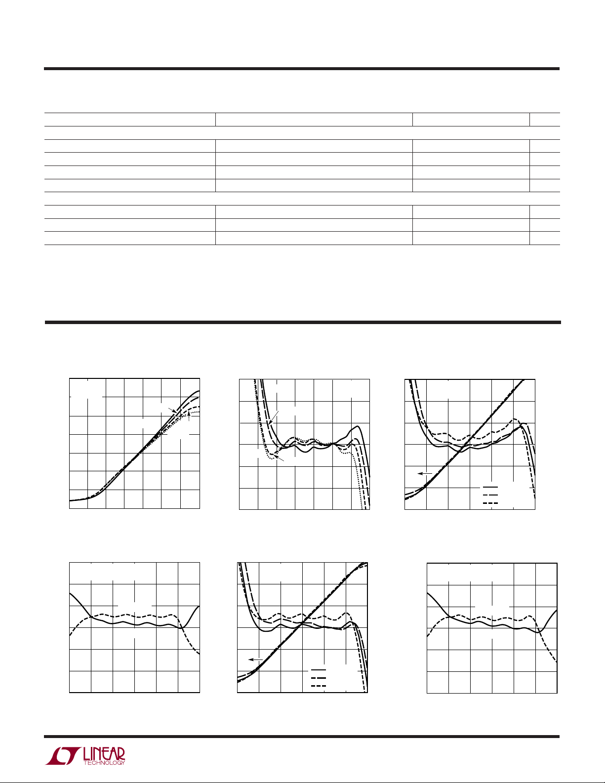
TYPICAL PERFOR A CE CHARACTERISTICS
Output Voltage vs Frequency
2.8
VCC = 3V
= 25°C
T
A
2.4
2.0
1.6
(V)
OUT
V
1.2
0.8
0.4
0
–70
–60 –50
Variation vs RF Input Power
V
OUT
3
VCC = 3V AT 50MHz
NORMALIZED AT 25°C
2
1
0
VARIATION (dB)
–1
OUT
V
–2
–3
–60
–50
RF INPUT POWER (dBm)
RF INPUT POWER (dBm)
–30 –10 0
–40 –20
TA = –40°C
TA = 85°C
–40 –30 –20
900MHz
50MHz
1.9GHz
2.5GHz
5534 G01
–10 0
5534 G04
Linearity Error vs Frequency Output Voltage vs RF Input Power
3
2
1
0
–1
LINEARITY ERROR (dB)
–2
–3
–70
50MHz
900MHz
2.5GHz
–60 –50
RF INPUT POWER (dBm)
1.9GHz
–30 –10 0
–40 –20
Output Voltage vs RF Input Power V
(V)
OUT
V
2.4
2.0
1.6
1.2
0.8
0.4
0
–60
VCC = 3V
AT 900MHz
–40 –30 –20
–50
RF INPUT POWER (dBm)
(Test circuit shown in Figure 1)
VCC = 3V
T
A
TA = 25°C
= 85°C
T
A
A
= –40C
T
–10 0
= 25°C
5534 G02
5534 G05
2.4
2.0
1.6
(V)
1.2
OUT
V
0.8
0.4
0
–60
3
2
LINEARITY ERROR (dB)
1
0
–1
–2
–3
VARIATION (dB)
OUT
V
–1
–2
–3
VCC = 3V
AT 50MHz
TA = 25°C
T
T
–40 –30 –20
–50
RF INPUT POWER (dBm)
Variation vs RF Input Power
OUT
3
VCC = 3V AT 900MHz
NORMALIZED AT 25°C
2
1
0
–60
–50
TA = –40°C
TA = 85°C
–40 –30 –20
RF INPUT POWER (dBm)
= 85°C
A
A
= –40C
–10 0
3
2
1
0
–1
–2
–3
5534 G03
–10 0
5534 G06
5534fa
LINEARITY ERROR (dB)
3

LT5534
UW
TYPICAL PERFOR A CE CHARACTERISTICS
(Test circuit shown in Figure 1)
Output Voltage vs RF Input Power V
2.4
2.0
1.6
(V)
1.2
OUT
V
0.8
0.4
0
–60
–50
Variation vs RF Input Power
OUT
3
VCC = 3V AT 2.5GHz
NORMALIZED AT 25°C
2
1
0
VARIATION (dB)
–1
OUT
V
–2
VCC = 3V
AT 1.9GHz
–40 –30 –20
RF INPUT POWER (dBm)
TA = –40°C
TA = 85°C
TA = 25°C
= 85°C
T
A
A = –40C
T
–10 0
3
2
LINEARITY ERROR (dB)
1
0
–1
–2
–3
5534 G07
Variation vs RF Input Power Output Voltage vs RF Input Power
OUT
3
VCC = 3V AT 1.9GHz
NORMALIZED AT 25°C
2
1
0
VARIATION (dB)
–1
OUT
V
–2
–3
–60
–50
TA = 85°C
TA = –40°C
–40 –30 –20
RF INPUT POWER (dBm)
Output Voltage vs RF Input Power
at V
= 3V and 5V
CC
2.8
TA = 25°C
2.4
V
CC
50MHz
= 3V, 5V
(V)
OUT
V
2.0
1.6
1.2
0.8
0.4
1.9GHz
= 3V, 5V
V
CC
–10 0
5534 G08
(V)
OUT
V
2.4
2.0
1.6
1.2
0.8
0.4
0
–60
VCC = 3V
AT 2.5GHz
–40 –30 –20
–50
RF INPUT POWER (dBm)
Output Voltage Distribution
vs TemperatureV
35
30
25
20
15
10
PERCENTAGE DISTRIBUTION (%)
RF P
IN
= 3V
V
CC
5
= –48dBm AT 1.9GHz
TA = 25°C
= 85°C
T
A
A = –40C
T
–10 0
5534 G09
TA = 25°C
= –40°C
T
A
= 85°C
T
A
3
2
LINEARITY ERROR (dB)
1
0
–1
–2
–3
–3
–60
–40 –30 –20
–50
RF INPUT POWER (dBm)
–10 0
5534 G10
0
–60
–30 –10 0
–40 –20
–50
RF INPUT POWER (dBm)
5534 G11
0
0.54
0.56
0.58
0.6
V
0.62
0.64 0.68
(V)
OUT
0.66
0.7
5534 G12
Output Voltage Distribution
vs Temperature
40
RF PIN = –14dBm AT 1.9GHz
= 3V
V
CC
35
30
25
20
15
10
PERCENTAGE DISTRIBUTION (%)
5
0
1.79
1.81
1.83
1.85
V
OUT
1.87
1.89 1.93
(V)
TA = 25°C
= –40°C
T
A
= 85°C
T
A
1.91
5534 G13
Supply Voltage vs Supply Current
10
9
TA = 85°C
8
TA = 25°C
7
6
SUPPLY CURRENT (mA)
5
4
2.5
3
TA = –40°C
3.5 4 4.5
SUPPLY VOLTAGE (V)
5 5.5
5530 G14
5534fa
4

UW
TYPICAL PERFOR A CE CHARACTERISTICS
RF Input Return Loss vs Frequency Output Transient Response
0
–5
1V/DIV
–10
–15
–20
RETURN LOSS (dB)
–25
–30
0
1 1.5 2
0.5
RF INPUT FREQUENCY (GHz)
2.5 3
5534 G15
(Test circuit shown in Figure 1)
V
OUT
RF
INPUT
50ns/DIV
PULSED RF
0dBm AT 100MHz
5534 G16
LT5534
U
UU
PI FU CTIO S
EN (Pin 1): Enable. When the input voltage is higher than
0.9V, the circuit is completely turned on. When the input
voltage is less than 0.6V, the circuit is turned off.
GND (Pins 2, 5): Ground.
(Pin 3): RF Detector Output.
V
OUT
W
BLOCK DIAGRA
DETDETDET
RF
6
RF LIMITERRF LIMITERRF LIMITER
V
(Pin 4): Power Supply. This pin should be decoupled
CC
using 100pF and 0.1µF capacitors.
RF (Pin 6): RF input. This pin is internally biased to
VCC – 0.18V. A coupling capacitor must be used to connect
to the RF signal source.
4
V
CC
DETDET
RF LIMITER
+
–
V
OUT
3
OFFSET
COMP
GND
2 5 1
BIAS
V
REF
EN
5534 BD
5534fa
5

LT5534
TEST CIRCUIT
C1
1nF
GND
V
6
RF
5
4
CC
R1
47Ω
OPTIONAL
C3
100pF
5534 F01
C2
0.1µF
J1
RF
V
CC
EN
R2
0Ω
V
OUT
OPTIONAL
C5
OPTIONAL
1
EN
LT5534
2
GND
3
V
OUT
REF DES
VALUE
SIZE
C1
1nF
C2
0.1µF
C3
100pF
C5
R1
47Ω
R2
0Ω
PART NUMBER
0402
AVX 04025C102JAT2A
0603
TAIYO YUDEN TMK107BJ104KA
0603
AVX 06035C101KAT2A
0603
OPTIONAL
0402
OPTIONAL
0603
OPTIONAL
Figure 1. Evaluation Circuit Schematic
Figure 2. Component Side Silkscreen of Evaluation Board
WUUU
APPLICATIO S I FOR ATIO
The LT5534 is a logarithmic-based detector, capable of
measuring an RF signal over the frequency range from
50MHz to 3GHz. The 60dB linear dynamic range is achieved
with very stable output over the full temperature range from
–40°C to 85°C. The absolute variation over temperature is
typically within ±1dB over a 47dB dynamic range at 1.9GHz.
RF Input Port
The RF port is internally biased at V
-0.18V. The pin
CC
should be DC blocked when connected to ground or other
6
Figure 3. Component Side Layout of Evaluation Board
matching components. A 47Ω resistor (R1) connected to
ground will provide better than 10dB input return loss up
to 2.5GHz. An additional 2nH inductance in series with R1
will provide improved input matching up to 3GHz. The
impedance vs frequency of the RF input is detailed in
Table 1.
The approximate linear RF input power range of the
LT5534 is from –62dBm to –2dBm with a 50Ω source
impedance. However, this range can be adjusted either
upward or downward to tailor for a particular application
5534fa

WUUU
APPLICATIO S I FOR ATIO
LT5534
Table 1. RF Input Impedance
FREQUENCY INPUT S11
(MHz) IMPEDANCE (Ω) MAG ANGLE (DEG)
50 1429-j429 0.938 –1.1
100 947-j710 0.934 –2.9
200 509-j609 0.922 –5.6
400 250-j440 0.908 –9.9
600 149-j344 0.900 –14.1
800 96.8-j278 0.896 –18.3
1000 67.6-j229 0.893 –22.7
1200 49.7-j193 0.889 –27.3
1400 38.4-j165 0.883 –32.3
1600 30.8-j143 0.879 –37.3
1800 25.4-j125 0.873 –42.6
2000 21.4-j109 0.866 –48.0
2200 18.5-j96.2 0.862 –53.6
2400 16.6-j85.0 0.848 –59.6
2600 15.2-j75.7 0.834 –65.6
2800 13.7-j67.5 0.826 –71.8
3000 12.1-j60.1 0.822 –78.2
need. By simply inserting an attenuator in front of the RF
input, the power range is shifted higher by the amount of
the attenuation. Moreover, due to the high RF input
impedance of the LT5534, the detecting range can be
moved downward for better detection sensitivity by using
a narrow band L-C matching network. By this means, the
sensitivity of the detector can be extended to as low as –
75dBm. By changing the value of resistor R1, the sensitivity of the detector can be fine-tuned within the range
from –75dBm to –62dBm. Though the range is adjustable, the overall linear dynamic range remains the same.
Output Interface
The output interface of the LT5534 is shown in Figure 4. The
output currents from the RF detectors are summed and
converted into an output voltage, V
. The maximum
OUT
charging current available to the output load is about 200µA.
The internal compensation capacitor C
is used to guaran-
C
tee stable operation for a large capacitive output load. The
slew rate is 133V/µs, and the small-signal output bandwidth
is approximately 30MHz when the output is resistively
V
CC
+
–
OUTPUT CURRENTS
FROM RF DETECTORS
Figure 4. Simplified Circuit Schematic
of the Output Interface
+
200µA
C
C
V
OUT
5534 F04
terminated or open. The fastest output transient response
is achieved when a large signal is applied to the RF input
port. See the output transient response plot in the Typical
Performance Characteristics section.
When the output is terminated with a load capacitance
, the slew rate is then limited to 200µA/(CL + 1.5pF). For
C
L
example, the slew rate is reduced to 17.4V/µs when C
=
L
10pF. A capacitive load may result in output voltage
overshoot, which can be minimized with a series compensation resistor R2 as shown in Figure 1. The suggested
resistor values for various capacitive loads are listed in
Table 2.
Table 2. Resistor Value for Capacitive Output
C5 (pF) R2 (kΩ)
1.5 5
54
10 2.5
20 2
The optional RC network at the output (R2 and C5 on the
demo board) can also provide further output filtering, if
needed. The output bandwidth is primarily dictated by the
RC constant of this lowpass filter when its corner frequency is less than 30MHz.
When a large signal (e.g., –2dBm) is present at the RF
input port, the output voltage swing can be as high as 2.4V.
To assure proper operation of the chip, the minimum
resistive load at the output termination should be greater
than 18kΩ.
Information furnished by Linear Technology Corporation is believed to be accurate and reliable.
However, no responsibility is assumed for its use. Linear Technology Corporation makes no representation that the interconnection of its circuits as described herein will not infringe on existing patent rights.
5534fa
7

LT5534
PACKAGE DESCRIPTIO
U
SC6 Package
6-Lead Plastic SC70
(Reference LTC DWG # 05-08-1638)
0.47
MAX
3.26 MAX
2.1 REF
RECOMMENDED SOLDER PAD LAYOUT
PER IPC CALCULATOR
0.10 – 0.40
NOTE:
1. DIMENSIONS ARE IN MILLIMETERS
2. DRAWING NOT TO SCALE
3. DIMENSIONS ARE INCLUSIVE OF PLATING
4. DIMENSIONS ARE EXCLUSIVE OF MOLD FLASH AND METAL BURR
0.65
REF
0.10 – 0.30
1.16 REF
0.96 MIN
1.80 – 2.40
0.10 – 0.18
(NOTE 3)
1.80 – 2.20
(NOTE 4)
INDEX AREA
1.15 – 1.35
(NOTE 4)
PIN 1
0.65 BSC
0.80 – 1.00
1.00 MAX
5. MOLD FLASH SHALL NOT EXCEED 0.254mm
6. DETAILS OF THE PIN 1 INDENTIFIER ARE OPTIONAL,
BUT MUST BE LOCATED WITHIN THE INDEX AREA
7. EIAJ PACKAGE REFERENCE IS EIAJ SC-70
(NOTE 6)
0.15 – 0.30
6 PLCS (NOTE 3)
0.00 – 0.10
REF
SC6 SC70 0802
RELATED PARTS
PART NUMBER DESCRIPTION COMMENTS
LT5504 800MHz to 2.7GHz RF Measuring Receiver 80dB Dynamic Range, Temperature Compensated, 2.7V to 5.25V
Supply
LT5506 500MHz Quadrature IF Demodulator with VGA 1.8V to 5.25V Supply, 40MHz to 500MHz IF, –4dB to 57dB Linear
Power Gain, 8.8MHz Baseband Bandwidth
LT5511 High Linearity Upconverting Mixer RF Output to 3GHz, 17dBm IIP3, Integrated LO Buffer
LT5512 DC-3GHz High Signal Level Downconverting Mixer DC to 3GHz, 21dBm IIP3, Integrated LO Buffer
LT5515 1.5GHz to 2.5GHz Direct Conversion Quadrature Demodulator 20dBm IIP3, Integrated LO Quadrature Generator
LT5516 0.8GHz to 1.5GHz Direct Conversion Quadrature Demodulator 21.5dBm IIP3, Integrated LO Quadrature Generator
LT5517 40MHz to 900MHz Direct Conversion Quadrature Demodulator 21dBm IIP3, Integrated LO Quadrature Generator
LT5519 0.7GHz to 1.4GHz High Linearity Upconverting Mixer 17.1dBm IIP3, 50Ω Single Ended RF and LO Ports
LT5520 1.3GHz to 2.3GHz High Linearity Upconverting Mixer 15.9dBm IIP3, 50Ω Single Ended RF and LO Ports
LT5522 600MHz to 2.7GHz High Linearity Downconverting Mixer 4.5V to 5.25V Supply, 25dBm IIP3 at 900MHz, NF = 12.5dB,
50Ω Single Ended RF and LO Ports
LTC®5532 300MHz to 7GHz Precision RF Power Detector Precision V
LT5546 500MHz Quadrature IF Demodulator with VGA and 17MHz 17MHz Baseband Bandwidth, 40MHz to 500MHz IF, 1.8V to 5.25V
Baseband Bandwidth Supply, –7dB to 56dB Linear Power Gain
Linear Technology Corporation
8
1630 McCarthy Blvd., Milpitas, CA 95035-7417
(408) 432-1900 ● FAX: (408) 434-0507
●
www.linear.com
Offset Control, Adjustable Gain and Offset
OUT
LT/LT 0905 REV A • PRINTED IN THE USA
© LINEAR TECHNOLOGY CORPORATION 2004
5534fa
 Loading...