

FEATURES
■
Wide Input Frequency Range: 0.8GHz to 2.5GHz*
■
Broadband LO and IF Operation
■
High Input IP3: +17.6dBm at 1900MHz
■
Typical Conversion Gain: –1.9dB at 1900MHz
■
High LO-RF and LO-IF Isolation
■
SSB Noise Figure: 15.1dB at 1900MHz
■
Single-Ended 50Ω RF and LO Interface
■
Integrated LO Buffer: –5dBm Drive Level
■
Low Supply Current: 28mA Typ
■
Enable Function
■
Single 5V Supply
■
16-Lead QFN (4mm × 4mm) Package
U
APPLICATIO S
■
Point-to-Point Data Communication Systems
■
Wireless Infrastructure
■
High Performance Radios
■
High Linearity Receiver Applications
LT5525
High Linearity, Low Power
Downconverting Mixer
U
DESCRIPTIO
The LT®5525 is a low power broadband mixer optimized
for high linearity applications such as point-to-point data
transmission, high performance radios and wireless infrastructure systems. The device includes an internally 50Ω
matched high speed LO amplifier driving a double-balanced active mixer core. An integrated RF buffer amplifier
provides excellent LO-RF isolation. The RF input balun and
all associated 50Ω matching components are integrated.
The IF ports can be easily matched across a broad range
of frequencies for use in a wide variety of applications.
The LT5525 offers a high performance alternative to
passive mixers. Unlike passive mixers, which require high
LO drive levels, the LT5525 operates at significantly lower
LO input levels and is much less sensitive to LO power
level variations.
, LTC and LT are registered trademarks of Linear Technology Corporation.
*Operation over a wider frequency range is achievable with reduced performance.
Consult factory for more information.
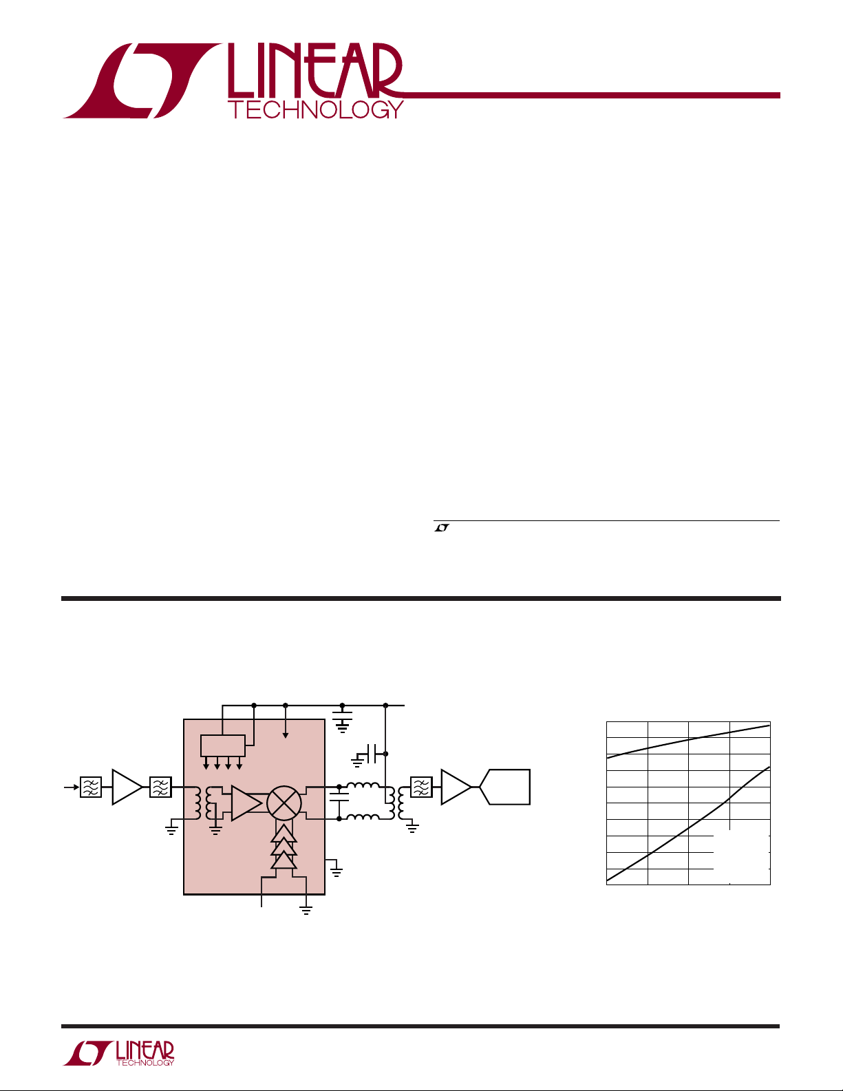
TYPICAL APPLICATIO
High Signal Level Frequency Downconversion
EN
BIAS
1900MHz
LNA VGA ADC
+
RF
–
RF
LT5525
LO INPUT
–5dBm
U
IF Output Power and IM3 vs
V
CC
5V DC
140MHz1900MHz
4:1
+
–
5525 TA01
0.01µF
100pF
150nH
1.2pF
150nH
V
V
CC2
CC1
IF
IF
GND
–
+
LO
LO
RF Input Power (Two Input Tones)
0
–10
–20
P
OUT
–30
–40
–50
–60
–10
TA = 25°C
= 1900MHz
f
RF
= 1760MHz
f
LO
= 140MHz
f
IF
= –5dBm
P
LO
–5
5525 TA02
–70
–80
OUTPUT POWER (dBm/TONE)
IM3
–90
–100
–15
–20
RF INPUT POWER (dBm/TONE)
0
5525f
1
LT5525
WW
W
ABSOLUTE MAXIMUM RATINGS
(Note 1)
Supply Voltage ...................................................... 5.5V
Enable Voltage ............................... –0.3V to V
LO Input Power ............................................... +10dBm
+
to LO– Differential DC Voltage ......................... ±1V
LO
+
LO
and LO– Common Mode DC Voltage... –0.5V to V
RF Input Power ................................................ +10dBm
RF+ to RF– Differential DC Voltage ..................... ±0.13V
+
RF
and RF– Common Mode DC Voltage ... –0.5V to V
IF+ and IF– Common Mode DC Voltage................... 5.5V
Operating Temperature Range ................ – 40°C to 85°C
Storage Temperature Range ................. –65°C to 125°C
Junction Temperature (TJ)................................... 125°C
U
+ 0.3V
CC
U
W
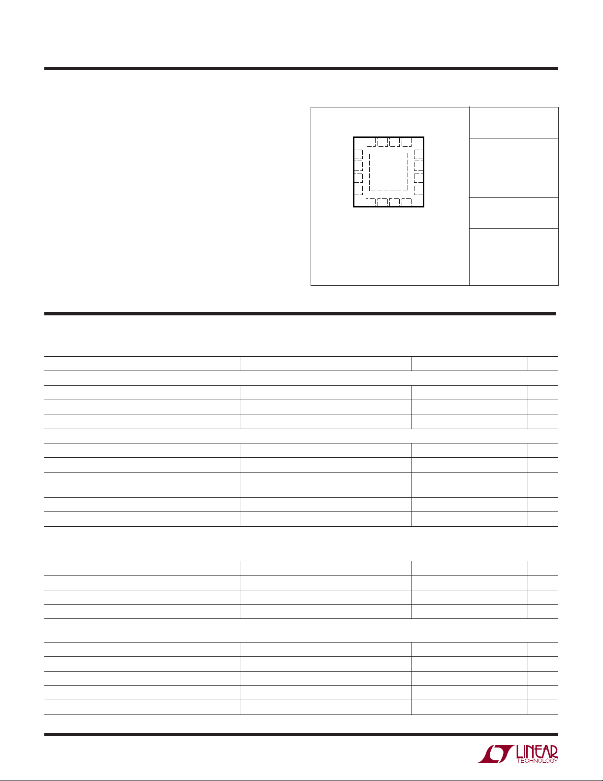
PACKAGE/ORDER INFORMATION
TOP VIEW
NC
LO+LO–NC
16 15 14 13
CC1VCC2
NC
12
GND
+
IF
11
–
IF
10
GND
9
1NC
+
RF
2
CC
CC
Consult LTC Marketing for parts specified with wider operating temperature ranges.
–
RF
NC
16-LEAD (4mm × 4mm) PLASTIC QFN
T
JMAX
EXPOSED PAD (PIN 17) IS GND,
MUST BE SOLDERED TO PCB.
NC PINS SHOULD BE GROUNDED
17
3
4
5 6 7 8
EN
V
UF PACKAGE
= 125°C, θJA = 37°C/W
ORDER PART
NUMBER
LT5525EUF
UF PART
MARKING
5525
U
DC ELECTRICAL CHARACTERISTICS
VCC = 5V, EN = 3V, TA = 25°C (Note 3), unless otherwise noted. Test circuit shown in Figure 1.
PARAMETER CONDITIONS MIN TYP MAX UNITS
Power Supply Requirements (VCC)
Supply Voltage (Note 6) 3.6 5 5.3 V
Supply Current VCC = 5V 28 33 mA
Shutdown Current EN = Low 100 µA
Enable (EN) Low = Off, High = On
EN Input High Voltage (On) 3V
EN Input Low Voltage (Off) 0.3 V
Enable Pin Input Current EN = 5V 55 µA
EN = 0V 0.1 µA
Turn-On Time (Note 5) 3 µs
Turn-Off Time (Note 5) 6 µs
AC ELECTRICAL CHARACTERISTICS
PARAMETER CONDITIONS MIN TYP MAX UNITS
RF Input Frequency Range (Note 4) Requires RF Matching Below 1300MHz 800 to 2500 MHz
LO Input Frequency Range (Note 4) 500 to 3000 MHz
IF Output Frequency Range (Note 4) Requires IF Matching 0.1 to 1000 MHz
VCC = 5V, EN = 3V, TA = 25°C. Test circuit shown in Figure 1. (Notes 2, 3)
PARAMETER CONDITIONS MIN TYP MAX UNITS
RF Input Return Loss ZO = 50Ω 15 dB
LO Input Return Loss ZO = 50Ω, External DC Blocks 15 dB
IF Output Return Loss ZO = 50Ω, External Match 15 dB
LO Input Power –10 to 0 dBm
(Notes 2, 3)
5525f
2

LT5525
AC ELECTRICAL CHARACTERISTICS
IIP3 tests, ∆f = 1MHz), f
= fRF – 140MHz, PLO = –5dBm, IF output measured at 140MHz, unless otherwise noted. Test circuit shown
LO
VCC = 5V, EN = 3V, TA = 25°C, PRF = –15dBm (–15dBm/tone for 2-tone
in Figure 1. (Notes 2, 3)
PARAMETER CONDITIONS MIN TYP MAX UNITS
Conversion Gain fRF = 900MHz –2.6 dB
= 1900MHz –1.9 dB
f
RF
= 2100MHz –2.0 dB
f
RF
f
= 2500MHz –2.0 dB
RF
Conversion Gain vs Temperature TA = –40°C to 85°C –0.020 dB/°C
Input 3rd Order Intercept fRF = 900MHz 21.0 dBm
= 1900MHz 17.6 dBm
f
RF
= 2100MHz 17.6 dBm
f
RF
f
= 2500MHz 12.0 dBm
RF
Single Sideband Noise Figure fRF = 900MHz 14.0 dB
= 1900MHz 15.1 dB
f
RF
= 2100MHz 15.6 dB
f
RF
f
= 2500MHz 15.6 dB
RF
LO to RF Leakage fLO = 500MHz to 1000MHz ≤–50 dBm
f
= 1000MHz to 3000MHz ≤–43 dBm
LO
LO to IF Leakage fLO = 500MHz to 1400MHz ≤–50 dBm
= 1400MHz to 3000MHz ≤–39 dBm
f
LO
RF to LO Isolation fRF = 500MHz to 3000MHz >38 dB
RF to IF Isolation fRF = 900MHz 62 dB
= 1900MHz 42 dB
f
RF
f
= 2100MHz 40 dB
RF
= 2500MHz 33 dB
f
RF
Input 1dB Compression fRF = 900MHz 7.6 dBm
= 1900MHz 4 dBm
f
RF
f
= 2100MHz 4 dBm
RF
= 2500MHz 3 dBm
f
RF
2RF-2LO Output Spurious Product 900MHz: fRF = 830MHz at –15dBm –63 dBc
= fLO + fIF/2) 1900MHz: fRF = 1830MHz at –15dBm –53 dBc
(f
RF
2100MHz: f
2500MHz: f
3RF-3LO Output Spurious Product 900MHz: fRF = 806.67MHz at –15dBm –74 dBc
= fLO + fIF/3) 1900MHz: fRF = 1806.67MHz at –15dBm –59 dBc
(f
RF
2100MHz: f
2500MHz: f
= 2030MHz at –15dBm –45 dBc
RF
= 2430Hz at –15dBm –42 dBc
RF
= 2006.67MHz at –15dBm –59 dBc
RF
= 2406.67Hz at –15dBm –60 dBc
RF
Note 1: Absolute Maximum Ratings are those values beyond which the life
of a device may be impaired.
Note 2: The performance is measured with the test circuit shown in
Figure 1. For 900MHz measurements, C1 = 3.9pF. For all other
measurements, C1 is not used.
Note 3: Specifications over the –40°C to 85°C temperature range are
assured by design, characterization and correlation with statistical process
controls.
Note 4: Operation over a wider frequency range is possible with reduced
performance. Consult the factory for information and assistance.
Note 5: Turn-on and turn-off times correspond to a change in the output
level of 40dB.
Note 6: The part is operable below 3.6V with reduced performance.
5525f
3
LT5525
RF INPUT POWER (dBm/TONE)
–20
–100
OUTPUT POWER (dBm/TONE)
–90
–70
–60
–50
0
–30
P
OUT
IM3
–15
–10
5525 G09
–80
–20
–10
–40
–5
0
25°C
85°C
–40°C
WU
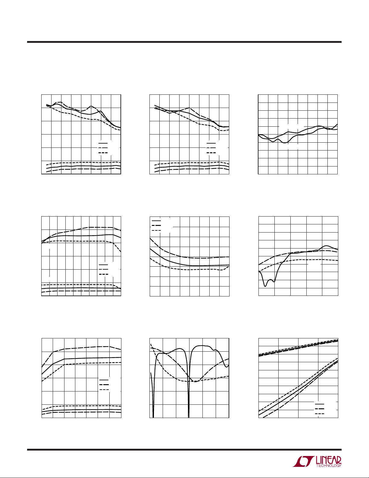
TYPICAL AC PERFOR A CE CHARACTERISTICS
= –15dBm (–15dBm/tone for 2-tone IIP3 tests, ∆f = 1MHz), fLO = fRF – 140MHz, PLO = –5dBm, IF output measured at 140MHz,
P
RF
unless otherwise noted. Test circuit shown in Figure 1.
VCC = 5V, EN = 3V, TA = 25°C, fRF = 1900MHz,
Conversion Gain and IIP3
vs RF Frequency (Low Side LO)
25
20
IIP3
15
10
5
GAIN (dB), IIP3 (dBm)
GAIN
0
–5
900
1300 1700
1100 1500
RF FREQUENCY (MHz)
1900
Conversion Gain and IIP3
vs LO Input Power
25
20
15
IIP3
10
5
GAIN (dB), IIP3 (dBm)
GAIN
0
–5
–12 –8 –4 0
LO INPUT POWER (dBm)
2100
25°C
85°C
–40°C
2300
25°C
85°C
–40°C
5525 G01
5525 G04
2500
4–14–16 –10 –6 –2 2
Conversion Gain and IIP3
vs RF Frequency (High Side LO)
25
20
IIP3
15
10
5
GAIN (dB), IIP3 (dBm)
GAIN
0
–5
900
1300 1700
1100 1500
RF FREQUENCY (MHz)
1900
SSB Noise Figure
vs LO Input Power
20
19
18
17
16
15
NOISE FIGURE (dB)
14
13
12
–14
25°C
85°C
–40°C
–12
–10
–8
LO INPUT POWER (dBm)
–6
–4
2100
–2
25°C
85°C
–40°C
2300
0
5525 G05
5525 G02
2500
2
SSB NF vs RF Frequency
20
19
18
17
16
15
14
NOISE FIGURE (dB)
13
12
11
12
900
HIGH SIDE LO
LOW SIDE LO
1100 1500
1300
RF FREQUENCY (MHz)
1700
1900
LO-IF, LO-RF and RF-LO Leakage
vs Frequency
0
–10
–20
–30
–40
LO-RF
–50
–60
LEAKAGE (dBm)
–70
–80
–90
–100
500
LO-IF
1000
FREQUENCY (MHz)
1500
RF-LO
2000
2100
2500
2300
2500
5525 G03
3000
5525 G06
Conversion Gain and IIP3
vs Supply Voltage
25
20
15
10
IIP3
5
GAIN (dB), IIP3 (dBm)
GAIN
0
–5
2.8
3.2 3.6
4
4 4.8
SUPPLY VOLTAGE (V)
25°C
85°C
–40°C
4.4 5.2 5.6
5525 G07
RF, LO and IF Port Return Loss
vs Frequency
0
–5
–10
–15
–20
RETURN LOSS (dB)
IF
–25
–30
0
RF
LO
1000 1500 2000
500
FREQUENCY (MHz)
IF Output Power and IM3 vs RF
Input Power (Two Input Tones)
2500 3000
5525 G08
5525f

LT5525
WU
TYPICAL AC PERFOR A CE CHARACTERISTICS
= –15dBm (–15dBm/tone for 2-tone IIP3 tests, ∆f = 1MHz), fLO = fRF – 140MHz, PLO = –5dBm, IF output measured at 140MHz,
P
RF
unless otherwise noted. Test circuit shown in Figure 1.
IF
, 2 × 2 and 3 × 3 Spurs
OUT
vs RF Input Power
10
0
–10
–20
–30
–40
–50
–60
–70
OUTPUT POWER (dBm)
–80
–90
–100
–20
IF OUT
= 1900MHz
f
RF
2RF-2LO
= 1830MHz
f
RF
–15 –5–10
RF INPUT POWER (dBm)
3RF-3LO
= 1806.67MHz
f
RF
TA = 25°C
f
f
= 1760MHz
LO
= 140MHz
IF
0
5525 G10
–30
–40
–50
–60
–70
–80
OUTPUT POWER (dBm)
–90
–100
VCC = 5V, EN = 3V, TA = 25°C, fRF = 1900MHz,
2 × 2 and 3 × 3 Spurs
vs LO Input Power
TA = 25°C
= 1760MHz
f
LO
= 140MHz
f
IF
2RF-2LO
= 1830MHz
f
RF
3RF-3LO
= 1806.67MHz
f
RF
–12 –8 –4 4
–16
LO INPUT POWER (dBm)
0
5525 G11
WU
TYPICAL DC PERFOR A CE CHARACTERISTICS
Test circuit shown in Figure 1.
Supply Current vs Supply Voltage Shutdown Current vs Supply Voltage
32
30
28
26
24
22
20
SUPPLY CURRENT (mA)
18
16
14
2.8
3.6
3.2
SUPPLY VOLTAGE (V)
25°C
85°C
–40°C
4 5.6
4.4
4.8 5.2
5525 G12
20
15
10
SHUTDOWN CURRENT (µA)
25°C
85°C
–40°C
5
0
2.8
3.2 3.6 4 4.4
SUPPLY VOLTAGE (V)
4.8 5.2 5.6
5525 G13
5525f
5

LT5525
U
UU
PI FU CTIO S
NC (Pins 1, 4, 8, 13, 16): Not Connected Internally. These
pins should be grounded on the circuit board for improved
LO-to-RF and LO-to-IF isolation.
RF+, RF– (Pins 2, 3): Differential Inputs for the RF Signal.
One RF input pin may be DC connected to a low impedance
ground to realize a 50Ω single-ended input at the other RF
pin. No external matching components are required. A DC
voltage should not be applied across these pins, as they
are internally connected through a transformer winding.
EN (Pin 5): Enable Pin. When the input voltage is higher
than 3V, the mixer circuits supplied through Pins 6, 7, 10
and 11 are enabled. When the input voltage is less than
0.3V, all circuits are disabled. Typical enable pin input
current is 55µA for EN = 5V and 0.1µA when EN = 0V.
V
(Pin 6): Power Supply Pin for the LO Buffer Circuits.
CC1
Typical current consumption is 11mA. This pin should be
externally connected to the other VCC pins and decoupled
with 1µF and 0.01µF capacitors.
V
(Pin 7): Power Supply Pin for the Bias Circuits.
CC2
Typical current consumption is 2.5mA. This pin should be
externally connected to the other VCC pins and decoupled
with 1µF and 0.01µF capacitors.
GND (Pins 9, 12): Ground. These pins are internally
connected to the Exposed Pad for better isolation. They
should be connected to ground on the circuit board,
though they are not intended to replace the primary
grounding through the Exposed Pad of the package.
–
and IF+ (Pins 10, 11): Differential Outputs for the IF
IF
Signal. An impedance transformation may be required to
match the outputs. These pins must be connected to V
CC
through impedance matching inductors, RF chokes or a
transformer center-tap.
–
LO
, LO+ (Pins 14, 15): Differential Inputs for the Local
Oscillator Signal. The LO input is internally matched to
50Ω. The LO can be driven with a single-ended source
through either LO input pin, with the other LO input pin
connected to ground. There is an internal DC resistance
across these pins of approximately 480Ω. Thus, a DC
blocking capacitor should be used if the signal source has
a DC voltage present.
Exposed Pad (Pin 17): Circuit Ground Return for the
Entire IC. This must be soldered to the printed circuit board
ground plane.
BLOCK DIAGRA
W
17
EXPOSED
PAD
LINEAR
+
RF
2
–
RF
3
AMPLIFIER
BIAS
EN
15 14
–
+
LO
LO
HIGH
SPEED
LO BUFFER
GND
12
+
IF
11
–
IF
10
DOUBLE-
BALANCED
MIXER
V
CC2
75
V
CC1
6
GND
9
5525 BD
5525f
6

TEST CIRCUITS
LT5525
LO
IN
1760MHz
16 15 14 13
+
–
LO
LO
GND
+
NC
IF
GND
IF
–
LT5525
V
CC1VCC2
56 78
C2
12
11
10
9
L3
C3
L2
C8
RF
1900MHz
C1
OPTIONAL
IN
900MHz INPUT MATCHING:
C1: 3.9pF
NC NC
17
1
NC
2
+
RF
3
–
RF
4
NC
EN
EN
REF DES VALUE SIZE PART NUMBER
C1 — 0402 Frequency Dependent
C2 0.01µF 0402 AVX 04023C103JAT
C3 1.2pF 0402 AVX 04025A1R2BAT
C4 100pF 0402 AVX 04025A101JAT
C8 1µF 0603 Taiyo Yuden LMK107BJ105MA
L2, L3 150nH 1608 Toko LL1608-FSR15J
T2 4:1 SM-22 M/A-COM ETC4-1-2
0.062"
ER = 4.4
0.018"
0.018"
T2
15
C4
2
3
V
CC
5526 F01
RF
GND
DC
GND
IF
4
OUT
140MHz
Figure 1. Test Schematic
WUUU
APPLICATIO S I FOR ATIO
T
he LT5525 consists of a double-balanced mixer, RF
balun, RF buffer amplifier, high speed limiting LO buffer
and bias/enable circuits. The IC has been optimized for
downconverter applications with RF input signals from
0.8GHz to 2.5GHz and LO signals from 500MHz to 3GHz.
With proper matching, the IF output can be operated at
frequencies from 0.1MHz to 1GHz. Operation over a
wider frequency range is possible, though with reduced
performance.
The RF, LO and IF ports are all differential, though the RF
and LO ports are internally matched to 50Ω for singleended drive. The LT5525 is characterized and production
tested using single-ended RF and LO inputs. Low side or
high side LO injection can be used.
RF Input Port
The mixer’s RF input, shown in Figure 2, consists of an
integrated balun and a high linearity differential amplifier.
The primary terminals of the balun are connected to the
RF+ and RF– pins (Pins 2 and 3, respectively). The secondary side of the balun is internally connected to the amplifier’s
differential inputs.
For single-ended operation, the RF+ pin is grounded and
the RF– pin becomes the RF input. It is also possible to
ground the RF– pin and drive the RF+ pin, if desired. If the
RF source has a DC voltage present, then a coupling
capacitor must be used in series with the RF input pin.
Otherwise, excessive DC current could damage the primary winding of the balun.
5525f
7

LT5525
WUUU
APPLICATIO S I FOR ATIO
+
RF
2
OPTIONAL SERIES
REACTANCE FOR
LOW BAND OR
HIGH BAND
RF
IN
MATCHING
–
RF
3
Figure 2. RF Input Schematic
As shown in Figure 3, the RF input return loss with no
external matching is greater than 12dB from 1.3GHz to
2.3GHz. The RF input match can be shifted down to
800MHz by adding a series 3.9pF capacitor at the RF input.
A series 1.2nH inductor can be added to shift the match up
to 2.5GHz. Measured return losses with these external
components are also shown in Figure 3.
0
–5
–10
–15
–20
RETURN LOSS (dB)
–25
–30
500
1000 1500 2000 2500
NO RF
MATCHING
SERIES 1.2nH
SERIES 3.9pF
RF FREQUENCY (MHz)
Figure 3. RF Input Return Loss Without and
with External Matching Components
Figure 4 illustrates the typical conversion gain, IIP3 and NF
performance of the LT5525 when the RF input match is
shifted lower in frequency using an external series 3.9pF
capacitor on the RF input.
RF input impedance and reflection coefficient (S11) versus frequency are shown in Table 1. The listed data is
referenced to the RF– pin with the RF+ pin grounded (no
external matching). This information can be used to simulate board-level interfacing to an input filter, or to design
a broadband input matching network.
LT5525
5525 F02
3000
5525 F03
25
20
IIP3
15
SSB NF
10
5
GAIN AND NF (dB), IIP3 (dBm)
0
GAIN
–5
800
900 1000
850 950
RF FREQUENCY (MHz)
T
= 25°C
A
= 140MHz
f
IF
LOW SIDE LO
HIGH SIDE LO
1100
1050
1150
1200
5525 F04
Figure 4. Typical Gain, IIP3 and NF with
Series 3.9pF Matching Capacitor
Table 1. RF Port Input Impedance vs Frequency
FREQUENCY INPUT REFLECTION COEFFICIENT
(MHz) IMPEDANCE MAG ANGLE
50 10.4 + j2.63 0.675 174
500 18.1 + j23.7 0.551 124
700 25.8 + j30.7 0.478 106
900 36.5 + j34.5 0.398 90
1100 48.4 + j33.3 0.321 74
1300 59.5 + j25.7 0.244 57
1500 65.9 + j13.1 0.177 33
1700 65.0 – j1.0 0.131 –3
1900 59.0 – j12.2 0.138 –47
2100 50.2 – j19.0 0.187 –79
2300 41.8 – j22.1 0.250 –97
2500 34.9 – j22.7 0.311 –109
2700 29.1 – j21.9 0.369 –118
3000 23.2 – j19.1 0.435 –130
A broadband RF input match can be easily realized by
using both the series capacitor and series inductor as
shown in Figure 5. This network provides good return loss
at both lower and higher frequencies simultaneously,
while maintaining good mid-band return loss. The broadband return loss is plotted in Figure 6. The return loss is
better than 12dB from 700MHz to 2.6GHz using the
element values of Figure 5.
LO Input Port
The LO buffer amplifier consists of high speed limiting
differential amplifiers designed to drive the mixer core for
high linearity. The LO+ and LO– pins are designed for
8
5525f
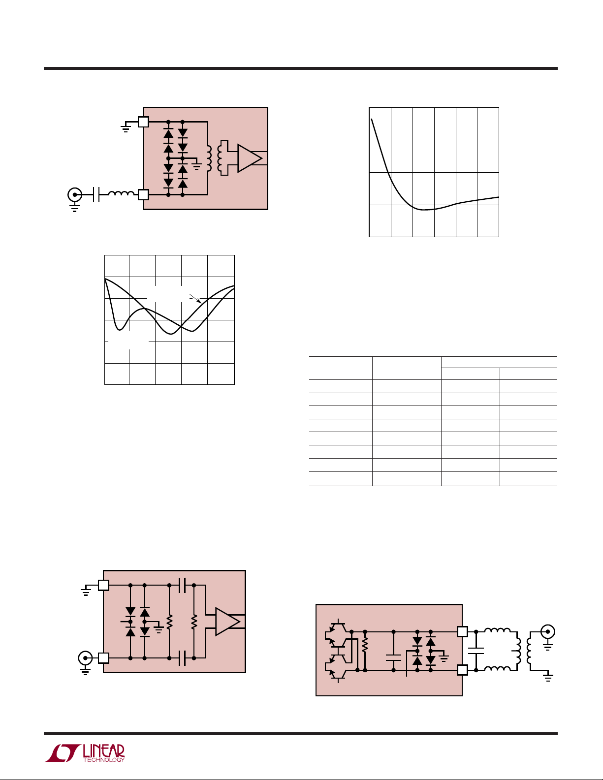
WUUU
FREQUENCY (MHz)
0
–20
RETURN LOSS (dB)
–15
–10
–5
0
500 1000 1500 2000
5525 F08
2500 3000
APPLICATIO S I FOR ATIO
LT5525
single-ended drive, though differential drive can be used if
desired. The LO input is internally matched to 50Ω. A
simplified schematic for the LO input is shown in Figure 7.
Measured return loss is shown in Figure 8.
If the LO source has a DC voltage present, then a coupling
capacitor should be used in series with the LO input pin
due to the internal resistive match.
+
RF
2
C5
4.7pF
L3
1.5nH
–
RF
3
RF
IN
Figure 5. Wideband RF Input Matching
0
–5
NO EXTERNAL
–10
–15
SERIES 1.5nH
–20
AND 4.7pF
RETURN LOSS (dB)
–25
–30
500
RF MATCHING
1000 1500 2000 2500
RF FREQUENCY (MHz)
Figure 6. RF Input Return Loss Using
Wideband Matching Network
–
LO
14
20pF
LO
50Ω
V
CC
IN
+
LO
15
480Ω
20pF
Figure 7. LO Input Schematic
54Ω
3000
5525 F06
LT5525
5525 F07
LT5525
5525 F05
Figure 8. LO Input Return Loss
The LO port input impedance and reflection coefficient
(S11) versus frequency are shown in Table 2. The listed
data is referenced to the LO+ pin with the LO– pin grounded.
Table 2. Single-Ended LO Input Impedance
FREQUENCY INPUT REFLECTION COEFFICIENT
(MHz) IMPEDANCE MAG ANGLE
100 93.1 – j121 0.686 –30
250 55.8 – j54 0.457 –57
500 47.7 – j28 0.276 –79
1000 42.3 – j14 0.171 –110
1500 38.5 – j9.3 0.166 –135
2000 35.8 – j7.8 0.187 –146
2500 34.8 – j7.8 0.281 –148
3000 34.2 – j8.7 0.214 –149
IF Output Port
A simplified schematic of the IF output circuit is shown in
Figure 9. The output pins, IF+ and IF–, are internally connected to the collectors of the mixer switching transistors.
Both pins must be biased at the supply voltage, which can
be applied through the center-tap of a transformer or
LT5525
5525 F09
L3
C3
V
CC
L2
575Ω
0.7pF
+
IF
11
–
IF
10
V
CC
Figure 9. IF Output with External Matching
4:1
IF
OUT
T2
5525f
9

LT5525
WUUU
APPLICATIO S I FOR ATIO
through impedance-matching inductors. Each IF pin draws
about 7.5mA of supply current (15mA total). For optimum
single-ended performance, these differential outputs must
be combined externally through an IF transformer or balun.
An equivalent small-signal model for the output is shown
in Figure 10. The output impedance can be modeled as a
574Ω resistor (RIF) in parallel with a 0.7pF capacitor. For
most applications, the bond-wire inductance (0.7nH per
side) can be ignored.
The external components, C3, L2 and L3 form an impedance transformation network to match the mixer output
impedance to the input impedance of transformer T2. The
values for these components can be estimated using the
equations below, along with the impedance values listed in
Table 3. As an example, at an IF frequency of 140MHz and
RL = 200Ω (using a 4:1 transformer for T2 with an external
50Ω load),
n = RIF/RL = 574/200 = 2.87
Q = √(n – 1) = 1.368
XC = RIF/Q = 420Ω
C = 1/(ω • XC) = 2.71pF
C3 = C – CIF = 2.01pF
XL = RL • Q = 274Ω
L2 = L3 = XL/2ω = 156nH
Table 3. IF Differential Impedance (Parallel Equivalent)
FREQUENCY OUTPUT REFLECTION COEFFICIENT
(MHz) IMPEDANCE MAG ANGLE
70 575|| – j3.39k 0.840 –1.8
140 574|| – j1.67k 0.840 –3.5
240 572|| – j977 0.840 –5.9
450 561|| – j519 0.838 –11.1
750 537|| – j309 0.834 –18.6
860 525|| – j267 0.831 –21.3
1000 509|| – j229 0.829 –24.8
1250 474|| – j181 0.822 –31.3
1500 435|| – j147 0.814 –38.0
LT5525
0.7nH L3
R
IF
574Ω
Figure 10. IF Output Small Signal Model
C
IF
0.7pF
0.7nH
+
IF
11
R
C3
–
IF
10
5525 F10
L
200Ω
L2
element network. This circuit is shown in Figure 11, where
L11, L12, C11 and C12 form a narrowband bridge balun.
These element values are selected to realize a 180° phase
shift at the desired IF frequency, and can be estimated
using the equations below. In this case, the load resistance, RL, is 50Ω.
RR
•
LL
11 12
==
IF L
ω
RR
ω
1
•
IF L
CC
11 12
==
I
nductor L13 or L14 provides a DC path between VCC and
the IF+ pin. Only one of these inductors is required. Low
cost multilayer chip inductors are adequate for L11, L12
and L13. If L14 is used instead of L13, a larger value is
usually required, which may require the use of a wirewound inductor. Capacitor C13 is a DC block which can
also be used to adjust the impedance match. Capacitor
C14 is a bypass capacitor.
C12
L14
OPT
L12
L11
C11
L13
OPT
C13
C14
IF
50Ω
5525 F11
OUT
+
IF
–
IF
V
CC
Low Cost Output Match
For low cost applications in which the required fractional
bandwidth of the IF output is less than 25%, it may be
possible to replace the output transformer with a lumped-
10
Figure 11. Narrowband Bridge IF Balun
Actual component values for IF frequencies of 240MHz,
360MHz and 450MHz are listed in Table 4. Typical IF port
return loss for these examples is shown in Figure 12.
5525f

WUUU
APPLICATIO S I FOR ATIO
LT5525
Conversion gain and IIP3 performance with an RF frequency of 1900MHz are plotted vs IF frequency in Figure
13. These results show that the usable IF bandwidth for the
lumped element balun is greater than 60MHz, assuming
tight tolerance matching components. Contact the factory
for applications assistance with this circuit.
0
–5
–10
–15
RETURN LOSS (dB)
–20
–25
200
300 350 400
250
FREQUENCY (MHz)
Figure 12. Typical IF Return Loss
Performance with 240MHz,
360MHz and 450MHz Lumped
Element Baluns
450 500
5525 F12
20
IIP3
15
10
5
GAIN (dB), IIP3 (dBm)
GAIN
0
–5
200
300 350 400
250
IF FREQUENCY (MHz)
Figure 13. Typical Gain and IIP3 vs
IF Frequency with 240MHz,
360MHz and 450MHz Lumped
Element Baluns
Table 4. Component Values for Lumped Balun
IF FREQ (MHz) L11, L12 (nH) C11, C12 (pF) C13 (pF) L14 (nH)
240 100 3.9 100 560
360 68 2.7 10 270
450 56 2.2 8.2 180
20
19
18
TA = 25°C
= fRF – f
f
LO
fRF = 1900MHz
P
P
= –5dBm
LO
= –15dBm
RF
450 500
IF
5525 F13
17
16
15
IIP3 (dBm)
14
13
TA = 25°C
12
f
PLO = –5dBm
11
P
10
1200
= fRF – f
LO
= –15dBm
RF
1400
IF
2000
1800
1600
RF FREQUENCY (MHz)
2200
240MHz
360MHz
450MHz
2400
5525 F14
Figure 14. Typical IIP3 vs RF
Frequency with Lumped Element
Baluns and IF Frequencies of
240MHz, 360MHz and 450MHz
2600
TYPICAL APPLICATIO S
Top Layer Silkscreen
U
Evaluation Board Layouts
Top Layer Metal
5525f
Information furnished by Linear Technology Corporation is believed to be accurate and reliable.
However, no responsibility is assumed for its use. Linear Technology Corporation makes no representation that the interconnection of its circuits as described herein will not infringe on existing patent rights.
11

LT5525
PACKAGE DESCRIPTIO
4.35 ± 0.05
2.15 ± 0.05
(4 SIDES)
2.90 ± 0.05
RECOMMENDED SOLDER PAD PITCH AND DIMENSIONS
NOTE:
1. DRAWING CONFORMS TO JEDEC PACKAGE OUTLINE MO-220 VARIATION (WGGC)
2. DRAWING NOT TO SCALE
3. ALL DIMENSIONS ARE IN MILLIMETERS
4. DIMENSIONS OF EXPOSED PAD ON BOTTOM OF PACKAGE DO NOT INCLUDE
MOLD FLASH. MOLD FLASH, IF PRESENT, SHALL NOT EXCEED 0.15mm ON ANY SIDE
U
0.30 ±0.05
0.65 BSC
UF Package
16-Lead Plastic QFN (4mm × 4mm)
(Reference LTC DWG # 05-08-1692)
4.00 ± 0.10
(4 SIDES)
0.72 ±0.05
PACKAGE
OUTLINE
PIN 1
TOP MARK
(NOTE 6)
0.75 ± 0.05
2.15 ± 0.10
(4-SIDES)
0.200 REF
0.00 – 0.05
5. EXPOSED PAD SHALL BE SOLDER PLATED
6. SHADED AREA IS ONLY A REFERENCE FOR PIN 1 LOCATION
ON THE TOP AND BOTTOM OF PACKAGE
R = 0.115
TYP
BOTTOM VIEW—EXPOSED PAD
0.55 ± 0.20
1615
1
2
(UF) QFN 1103
0.30 ± 0.05
0.65 BSC
RELATED PARTS
PART NUMBER DESCRIPTION COMMENTS
Infrastructure
LT5512 DC-3GHz High Signal Level Down Converting Mixer 21dBm IIP3, Integrated LO Buffer
LT5514 Ultralow Distortion, IF Amplifier/ADC Driver with Digitally 850MHz Bandwidth, 47dBm OIP3 at 100MHz, 10.5dB to 33dB Gain
Controlled Gain Control Range
LT5519 0.7GHz to 1.4GHz High Linearity Upconverting Mixer 17.1dBm IIP3 at 1GHz, Integrated RF Output Transformer with 50Ω
LT5520 1.3GHz to 2.3GHz High Linearity Upconverting Mixer 15.9dBm IIP3 at 1.9GHz, Integrated RF Output Transformer with 50Ω
LT5521 3.7GHz Very High Linearity Mixer 24.2dBm IIP3 at 1.95GHz, 12.5dB SSBNF, –42dBm LO Leakage,
LT5522 600MHz to 2.7GHz High Signal Level Downconverting Mixer 4.5V to 5.25V Supply, 25dBm IIP3 at 900MHz, NF = 12.5dB,
LT5526 High Linearity, Low Power Downconverting Mixer 16.5dBm IIP3 at 900MHz, NF = 11dB, Supply Current = 28mA, 3.6V
RF Power Detectors
LTC5508 300MHz to 7GHz RF Power Detector 44dB Dynamic Range, Temperature Compensated, SC70 Package
LTC5532 300MHz to 7GHz Precision RF Power Detector Precision V
LT5534 50MHz to 3GHz RF Power Detector with 60dB Dynamic Range ±1dB Output Variation over Temperature, 38ns Response Time
LTC5535 600MHz to 7GHz RF Power Detector 12MHz Baseband BW, Precision Offset with Adjustable Gain and Offset
Wide Bandwidth ADCs
LTC1749 12-Bit, 80Msps ADC 500MHz BW S/H, 71.8dB SNR, 87dB SFDR
LTC1750 14-Bit, 80Msps ADC 500MHz BW S/H, 75.5dB SNR, 90dB SFDR, 2.25V
LTC2222/ 12-Bit, 105Msps/80Msps ADC Low Power 775MHz BW S/H, 61dB SNR, 75dB SFDR ±0.5V or ±1V
LTC2223 Input
LTC2224/ 10-Bit/12-Bit, 135Msps ADC Low Power 775MHz BW S/H, 61dB SNR, 75dB SFDR ±0.5V or ±1V
LTC2234 Input
Linear Technology Corporation
12
1630 McCarthy Blvd., Milpitas, CA 95035-7417
(408) 432-1900 ● FAX: (408) 434-0507
●
www.linear.com
Matching, Single-Ended LO and RF Ports Operation
Matching, Single-Ended LO and RF Ports Operation
Supply Voltage = 3.15V to 5.25V
50Ω Single-Ended RF and LO Ports
to 5.3V Supply
Offset Control, Adjustable Gain and Offset
OUT
P-P
Input Ranges
LT/TP 1004 1K • PRINTED IN THE USA
© LINEAR TECHNOLOGY CORPORATION 2004
or 1.35V
P-P
5525f
 Loading...