

LO INPUT POWER (dBm)
–11
0
G
C
, SSB NF (dB), IIP3 (dBm)
4
8
12
16
–9 –7 –5 –3
5522 TA01
–1 1
20
IIP3
24
22
IF = 140MHz
LOW-SIDE LO
T
A
= 25°C
V
CC
= 5V
2
6
10
14
18
–70
–60
LO-RF LEAKAGE (dBm)
–50
–40
–30
–20
–10
SSB NF
LO-RF
FEATURES
■
Internal On-Chip RF Input Transformer
■
50Ω Single-Ended RF and LO Ports
■
High Input IP3: +25dBm at 900MHz
+21.5dBm at 1900MHz
■
Low Power Consumption: 280mW Typical
■
Integrated LO Buffer: Low LO Drive Level
■
High LO-RF and LO-IF Isolation
■
Wide RF Frequency Range: 0.4GHz to 2.7GHz*
■
Very Few External Components
■
Enable Function
■
4.5V to 5.25V Supply Voltage Range
■
16-Lead (4mm × 4mm) QFN Package
U
APPLICATIO S
■
Cellular, PCS and UMTS Band Infrastructure
■
CATV Downlink Infrastructure
■
2.4GHz ISM
■
High Linearity Downmixer Applications
LT5522
400MHz to 2.7GHz
High Signal Level
Downconverting Mixer
U
DESCRIPTIO
The LT®5522 active downconverting mixer is optimized for
high linearity downconverter applications including cable
and wireless infrastructure. The IC includes a high speed
differential LO buffer amplifier driving a double-balanced
mixer. The LO buffer is internally matched for wideband,
single-ended operation with no external components.
The RF input port incorporates an integrated RF transformer and is internally matched over the 1.2GHz to 2.3GHz
frequency range with no external components. The RF
input match can be shifted down to 400MHz, or up to
2.7GHz, with a single shunt capacitor or inductor, respectively. The high level of integration minimizes the total
solution cost, board space and system-level variation.
The LT5522 delivers high performance and small size
without excessive power consumption.
, LTC and LT are registered trademarks of Linear Technology Corporation.
All other trademarks are the property of their respective owners.
*Operation over a wider frequency range is possible with reduced performance.
Consult factory for information and assistance.
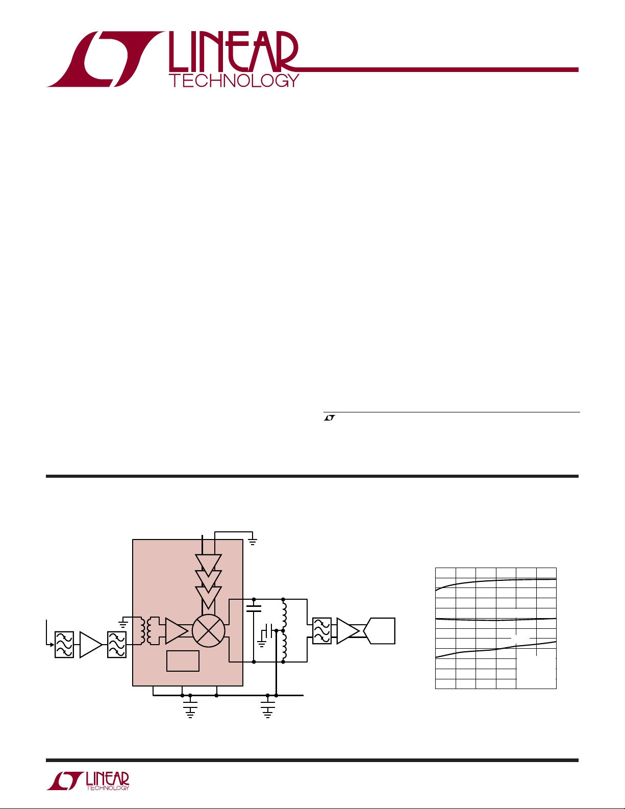
TYPICAL APPLICATIO
1850MHz
TO
1910MHz
U
LO INPUT
–5dBm
–
+
LO
LT5522
+
RF
LNA
Figure 1. High Signal Level Downmixer for Wireless Infrastructure
RF
–
CONTROL
EN V
BIAS/
CC1
LO
+
IF
2.7pF
100pF
–
IF
V
CC2
0.01µF 3.3µF
150nH
150nH
140MHz
5V
(TYP)
VGA
LTC1748
ADC
5522 F01
1.9GHz Conversion Gain, IIP3, SSB
NF and LO-RF Leakage vs LO Power
5522fa
1
LT5522
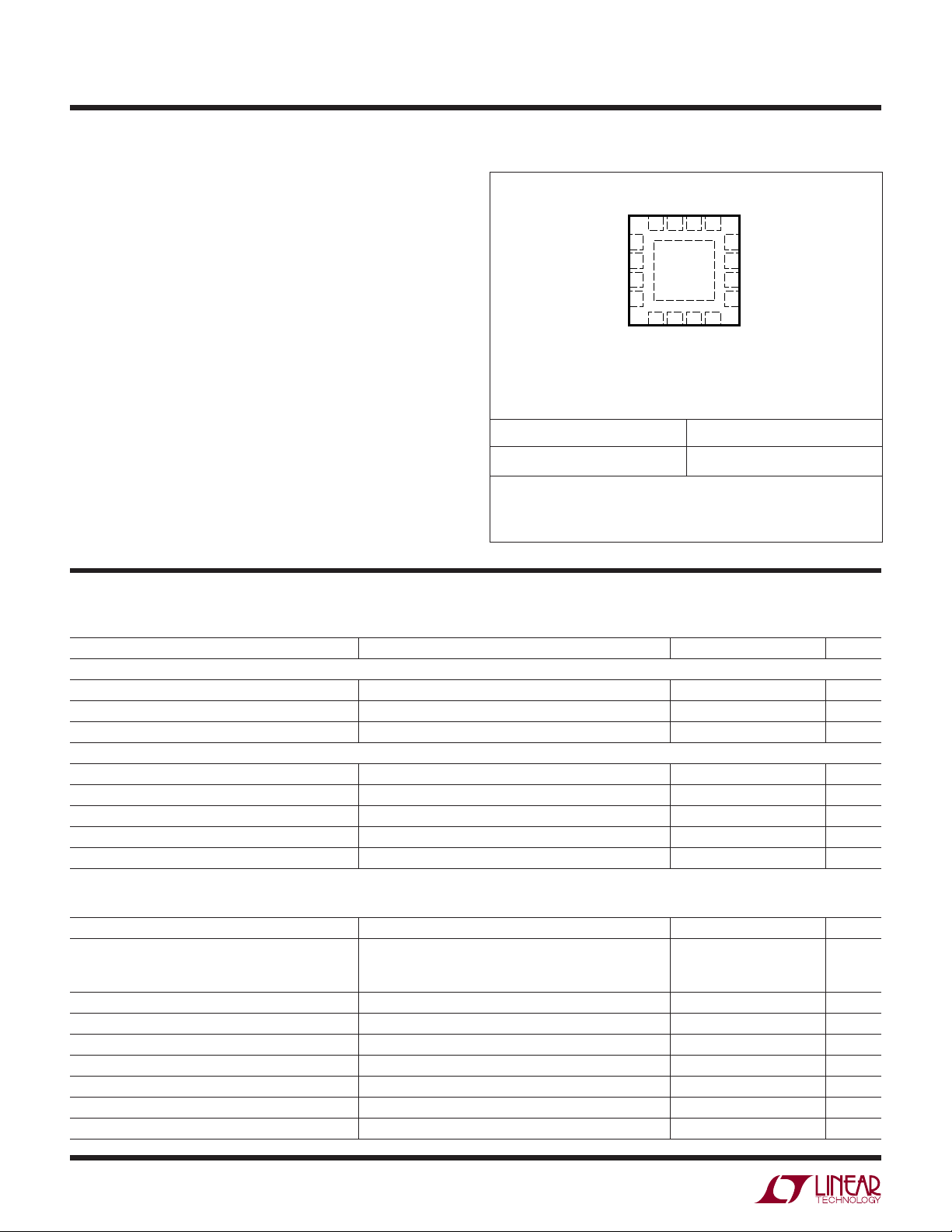
PACKAGE/ORDER I FOR ATIO
UU
W
WWWU
ABSOLUTE AXI U RATI GS
(Note 1)
Supply Voltage ...................................................... 5.5V
Enable Voltage ............................... – 0.3V to V
LO Input Power ............................................... +10dBm
+
LO
to LO– Differential DC Voltage ......................... ±1V
LO Input DC Common Mode Voltage ...................... ±1V
RF Input Power ................................................ +10dBm
RF+ to RF– Differential DC Voltage ........................ ±0.2V
RF Input DC Common Mode Voltage ...................... ±1V
Operating Temperature Range ................ –40°C to 85°C
Storage Temperature Range ................. –65°C to 125°C
Junction Temperature (T
).................................... 125°C
J
+ 0.3V
CC
TOP VIEW
NC
LO+LO–NC
16 15 14 13
GND
1NC
+
RF
2
–
RF
3
NC
4
5 6 7 8
EN
16-LEAD (4mm × 4mm) PLASTIC QFN
EXPOSED PAD (PIN 17) IS GND, MUST BE SOLDERED TO PCB
UF PACKAGE
T
= 125°C, θJA = 37°C/W
JMAX
ORDER PART NUMBER
17
V
12
+
IF
11
–
IF
10
GND
9
NC
CC1
CC2
V
UF PART MARKING
LT5522EUF 5522
Order Options Tape and Reel: Add #TR
Lead Free: Add #PBF Lead Free Tape and Reel: Add #TRPBF
Lead Free Part Marking: http://www.linear.com/leadfree/
Consult LTC Marketing for parts specified with wider operating temperature ranges.
DC ELECTRICAL CHARACTERISTICS
(Test circuit shown in Figure 2) VCC = 5VDC, EN = high, TA = 25°C,
unless otherwise noted. (Note 3)
PARAMETER CONDITIONS MIN TYP MAX UNITS
Power Supply Requirements (VCC)
Supply Voltage 4.5 5 5.25 VDC
Supply Current VCC = 5V 56 68 mA
Shutdown Current EN = Low 100 µA
Enable (EN) Low = Off, High = On
Input High Voltage (On) 3 VDC
Input Low Voltage (Off) 0.3 VDC
Enable Pin Input Current EN = 5VDC 55 75 µA
Turn On Time 3 µs
Turn Off Time 5 µs
AC ELECTRICAL CHARACTERISTICS
PARAMETER CONDITIONS MIN TYP MAX UNITS
RF Input Frequency Range Shunt Capacitor on Pin 3 (Low Band) 400 MHz
No External Matching (Mid Band) 1200 to 2300 MHz
Shunt Inductor on Pin 3 (High Band) 2700 MHz
LO Input Frequency Range No External Matching 400 2700 MHz
IF Output Frequency Range Requires Appropriate IF Matching 0.1 to 1000 MHz
RF Input Return Loss ZO = 50Ω 15 dB
LO Input Return Loss ZO = 50Ω 13 dB
IF Output Return Loss ZO = 50Ω 18 dB
LO Input Power –10 –5 0 dBm
RF to LO Isolation 50MHz to 2700MHz >45 dB
(Notes 2, 3) (Test circuit shown in Figure 2).
5522fa
2
LT5522
AC ELECTRICAL CHARACTERISTICS
= 25°C, PRF = –7dBm (–7dBm/tone for 2-tone IIP3 tests, ∆f = 1MHz), fLO = fRF – 140MHz, PLO = –5dBm, IF output measured at
T
A
Cellular/PCS/UMTS downmixer application: VCC = 5V, EN = high,
140MHz, unless otherwise noted. (Notes 2, 3) (Test circuit shown in Figure 2).
PARAMETER CONDITIONS MIN TYP MAX UNITS
Conversion Gain RF = 450MHz, High Side LO –2.0 dB
RF = 900MHz –0.5 dB
RF = 1800MHz –2 –0.2 dB
RF = 1900MHz –0.1 dB
RF = 2100MHz 0.2 dB
RF = 2450MHz –0.7 dB
Conversion Gain vs Temperature TA = –40° C to 85°C –0.02 dB/°C
Input 3rd Order Intercept RF = 450MHz, High Side LO 22.3 dBm
RF = 900MHz 25.0 dBm
RF = 1800MHz 21.8 dBm
RF = 1900MHz 21.5 dBm
RF = 2100MHz 20.0 dBm
RF = 2450MHz 16.8 dBm
Single Sideband Noise Figure (Note 4) RF = 900MHz 12.5 dB
RF = 1800MHz 13.9 dB
RF = 2100MHz 14.3 dB
RF = 2450MHz 15.6 dB
LO to RF Leakage fLO = 400MHz to 2700MHz ≤–50 dBm
LO to IF Leakage fLO = 400MHz to 2700MHz ≤–49 dBm
2RF-2LO Output Spurious Product (fRF = fLO + fIF/2) 900MHz: fRF = 830MHz at –12dBm –73 dBc
1900MHz: f
3RF-3LO Output Spurious Product (fRF = fLO + fIF/3) 900MHz: fRF = 806.67MHz at –12dBm –72 dBc
1900MHz: fRF = 1806.67MHz at –12dBm –65 dBc
Input 1dB Compression RF = 450MHz, High Side LO 12.0 dBm
RF = 900MHz 10.8 dBm
RF = 1900MHz 8.0 dBm
= 1830MHz at –12dBm –60 dBc
RF
1150MHz CATV infrastructure application: VCC = 5V, EN = high, TA = 25°C, RF input = 1150MHz at –12dBm (–12dBm/tone for 2-tone
IIP3 tests, ∆f = 1MHz), LO input swept from 1200MHz to 2200MHz, P
= –5dBm, IF output measured from 50MHz to 1050MHz unless
LO
otherwise noted. (Note 3) (Test circuit shown in Figure 3).
PARAMETER CONDITIONS MIN TYP MAX UNITS
Conversion Gain fLO = 1650MHz, fIF = 500MHz –0.6 dB
Input 3rd Order Intercept fLO = 1650MHz, fIF = 500MHz 23 dBm
Single Sideband Noise Figure (Note 4) fLO = 1650MHz, fIF = 500MHz 14.3 dB
LO to RF Leakage fLO = 1200MHz to 2200MHz ≤– 51 dBm
LO to IF Leakage fLO = 1200MHz to 2200MHz ≤– 45 dBm
2RF – LO Output Spurious Product PRF = –12dBm (Single Tone), 50MHz ≤ fIF ≤ 900MHz ≤ –63 dBc
2RF1 – LO Output Spurious Product 2 –68 dBc
2RF2 – LO Output Spurious Product –68 dBc
(RF1 + RF2) – LO Output Spurious Product –63 dBc
RF Input Return Loss 950MHz to 1350MHz, ZO = 50Ω >15 dB
LO Input Return Loss 1200MHz to 2200MHz, ZO = 50Ω 13 dB
IF Output Return Loss 50MHz to 1050MHz, ZO = 50Ω 10 dB
Note 1: Absolute Maximum Ratings are those values beyond which the life
of a device may be impaired.
Note 2: 450MHz, 900MHz and 2450MHz performance measured with the
following external RF input matching. 450MHz: C5 = 8.2pF, 5mm away
from Pin 3 on the 50Ω input line. 900MHz: C5 = 2.2pF at Pin 3. 2450MHz:
L3 = 3.9nH at Pin 3. See Figure 2.
2-Tone 2nd Order Spurious Outputs
RF1 = 1147MHz, RF2 = 1153MHz, –15dBm/Tone
LO = 1650MHz, Spurs at 644MHz, 656MHz and 650MHz
Note 3: Specifications over the –40°C to 85°C operating temperature
range are assured by design, characterization and correlation with
statistical process controls.
Note 4: SSB Noise Figure measurements performed with a small-signal noise
source and bandpass filter on RF input, and no other RF signal applied.
5522fa
3
LT5522
WU
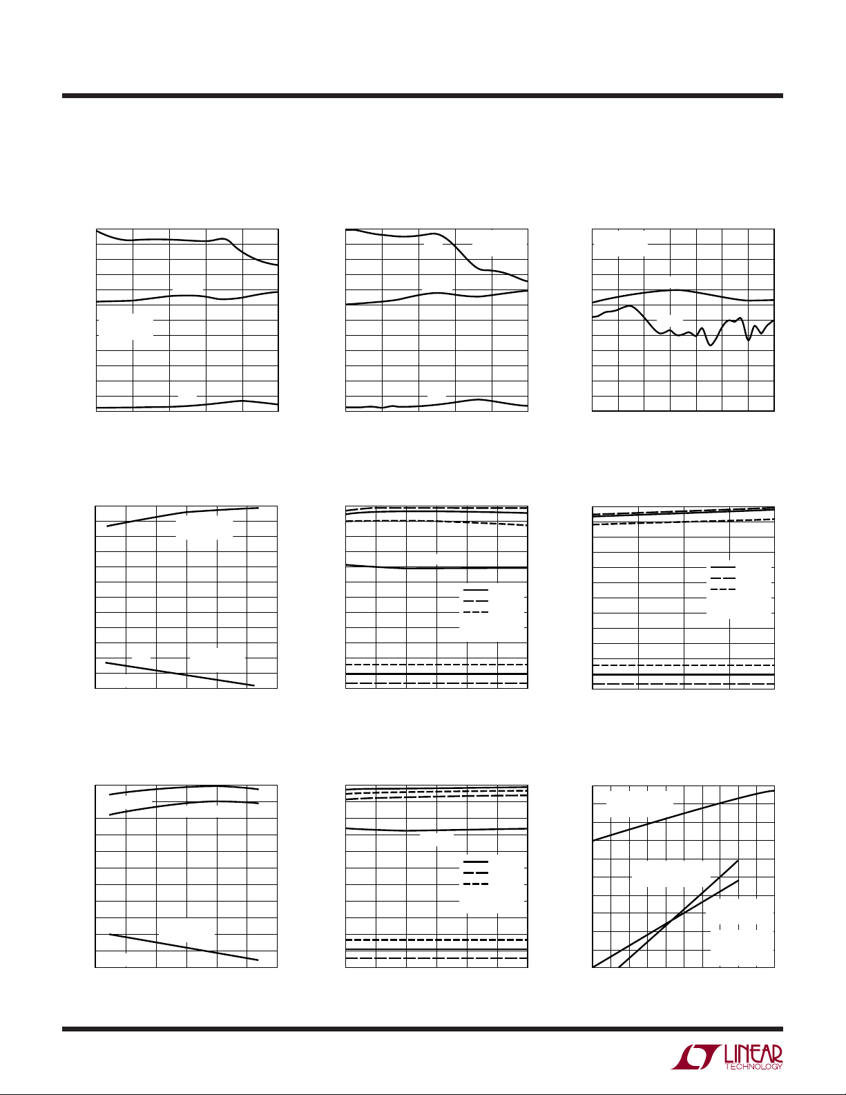
TYPICAL AC PERFOR A CE CHARACTERISTICS
V
= 5V, EN = High, TA = 25°C, PRF = –7dBm (–7dBm/tone for 2-tone IIP3 tests, ∆f = 1MHz), PLO = –5dBm, IF output measured
CC
at 140MHz, unless otherwise noted. (Test circuit shown in Figure 2).
Mid-band RF (no external RF matching)
Conv Gain, IIP3 and SSB NF
vs RF Frequency (Low Side LO)
23
21
19
17
15
13
TA = 25°C
11
= 140MHz
f
IF
9
7
5
AND SSB NF (dB), IIP3 (dBm)
C
G
3
1
–1
1300
1500
IIP3
SSB NF
G
C
1900
1700
RF FREQUENCY (MHz)
Conv Gain and IIP3
vs Temperature (RF = 1800MHz)
22
20
18
16
14
12
10
8
(dB), IIP3 (dBm)
C
6
G
4
2
0
= 140MHz
f
IF
–2
–50
–25
IIP3
G
LOW SIDE LO
HIGH SIDE LO
C
TEMPERATURE (°C)
LOW SIDE LO
HIGH SIDE LO
02550
2100
75 100
5522 G01
5522 G04
2300
Conv Gain, IIP3 and SSB NF
vs RF Frequency (High Side LO) LO Leakage vs LO Frequency
23
21
19
17
15
13
11
9
7
5
AND SSB NF (dB), IIP3 (dBm)
C
G
3
1
–1
1300
1500
IIP3
SSB NF
G
C
1900
1700
RF FREQUENCY (MHz)
Conv Gain, IIP3 and SSB NF
vs LO Power (RF = 1800MHz)
22
20
18
16
14
12
10
8
6
4
AND SSB NF (dB), IIP3 (dBm)
C
G
2
0
–2
–11
IIP3
SSB NF
G
C
–7 –5 –3
–9
LO INPUT POWER (dBm)
TA = 25°C
= 140MHz
f
IF
2100
f
= 1660MHz
LO
= 140MHz
f
IF
2300
5522 G02
25°C
85°C
–40°C
–1 1
5522 G05
–30
TA = 25°C
–35
= 140MHz
f
IF
–40
–45
–50
–55
–60
–65
–70
LO LEAKAGE (dBm)
–75
–80
–85
–90
1100
1300
LO-RF
LO-IF
1900
1700
1500
LO FREQUENCY (MHz)
Conv Gain and IIP3 vs Supply
Voltage (RF = 1800MHz)
22
20
18
16
14
12
10
8
(dB), IIP3 (dBm)
C
6
G
4
G
2
0
–2
4.5
IIP3
C
4.75
SUPPLY VOLTAGE (V)
5 5.25
2100
2300
5522 G03
25°C
85°C
–40°C
fLO = 1660MHz
= 140MHz
f
IF
5522 G06
2500
5.5
Conv Gain and IIP3
vs Temperature (RF = 2100MHz)
20
18
LOW SIDE LO
16
IIP3
14
12
10
8
(dB), IIP3 (dBm)
6
C
G
4
G
C
2
0
= 140MHz
f
IF
–2
–50
–25
HIGH SIDE LO
LOW SIDE LO
HIGH SIDE LO
02550
TEMPERATURE (°C)
4
75 100
5522 G07
Conv Gain, IIP3 and SSB NF
vs LO Power (RF = 2100MHz)
20
18
IIP3
16
14
12
10
8
6
4
AND SSB NF (dB), IIP3 (dBm)
G
C
C
2
G
0
–2
–11
–9
SSB NF
–7 –5 –3
LO INPUT POWER (dBm)
f
= 1960MHz
LO
= 140MHz
f
IF
25°C
85°C
–40°C
–1 1
5522 G08
IF OUT, 2 × 2 and 3 × 3 Spurs
vs RF Input Power (Single Tone)
10
0
–10
–20
–30
–40
–50
–60
OUTPUT POWER (dBm)
–70
–80
–90
–21
IF OUT
(RF = 1900MHz)
(RF = 1806.67MHz)
–15–18
–9–12
RF INPUT POWER (dBm)
3RF-3LO
–3 0 6
–6
2RF-2LO
(RF = 1830MHz)
TA = 25°C
= 1760MHz
f
LO
= 140MHz
f
IF
3
5522 G09
5522fa
9
WU
TYPICAL AC PERFOR A CE CHARACTERISTICS
(L3 = 3.9nH) V
measured at 140MHz, unless otherwise noted. (Test circuit shown in Figure 2).
= 5V, EN = High, TA = 25°C, PRF = –7dBm (–7dBm/tone for 2-tone IIP3 tests, ∆f = 1MHz), PLO = –5dBm, IF output
CC
LT5522
Low-band RF (C5 = 2.2pF) and high-band RF
Low Band Conv Gain, IIP3 and
SSB NF vs RF Frequency
18
16
HIGH SIDE LO
14
12
10
8
(dB)
C
G
6
4
–2
2
0
600
TA = 25°C
= 140MHz
f
IF
HIGH SIDE LO
LOW SIDE LO
G
C
700
RF FREQUENCY (MHz)
800
LOW SIDE LO
900 1000
1100
Low Band Conv Gain, IIP3 and SSB
NF vs LO Power (RF = 900MHz)
17
15
13
11
9
7
(dB)
C
G
5
3
1
–1
–3
–11
SSB NF
G
C
–9
–7
LO INPUT POWER (dBm)
–5 –3
25°C
85°C
–40°C
fLO = 760MHz
= 140MHz
f
IF
–1
IIP3
SSB NF
5522 G10
IIP3
5522 G13
17
26
24
15
13
22
SSB NF (dB), IIP3 (dBm)
20
11
9
18
7
16
(dB)
C
G
5
14
3
12
1
–1
–3
SSB NF (dB), IIP3 (dBm)
LO LEAKAGE (dBm)
1200
1
10
8
6
26
24
22
20
18
16
14
12
10
8
6
Low Band Conv Gain and IIP3
vs Temperature (RF = 900MHz)
LOW SIDE LO
HIGH SIDE LO
G
C
fIF = 140MHz
–25
–50
LOW SIDE LO
HIGH SIDE LO
25 50
0
TEMPERATURE (°C)
75
LO Leakage vs LO Frequency
(Low Band RF Match)
–30
TA = 25°C
–35
= 140MHz
f
IF
= –5dBm
P
–40
LO
–45
–50
–55
–60
–65
–70
–75
–80
–85
–90
400
LO-IF
LO-RF
600
800
LO FREQUENCY (MHz)
1000
5522 G11
1200
IIP3
100
5522 G14
26
24
–10
22
–20
20
–30
IIP3 (dBm)
18
–40
16
–50
14
–60
12
–70
OUTPUT POWER (dBm)
10
–80
8
–90
6
–100
17
15
13
11
9
7
(dB)
C
G
5
3
1
–1
–3
1400
Low Band IF OUT, 2 × 2 and 3 × 3
Spurs vs RF Input Power (Single Tone)
10
0
IF OUT
(RF = 900MHz)
(RF = 806.67MHz)
–9
–15
–12–18
RF INPUT POWER (dBm)
3RF-3LO
–6
2RF-2LO
(RF = 830MHz)
–3
0
TA = 25°C
= 760MHz
f
LO
3
6
9
5522 G12
12
Low Band Conv Gain and IIP3 vs
Supply Voltage (RF = 900MHz)
IIP3
25°C
85°C
–40°C
fLO = 760MHz
= 140MHz
f
IF
G
C
4.5
4.75 5
SUPPLY VOLTAGE (V)
5.25
5.5
5522 G15
26
24
22
20
IIP3 (dBm)
18
16
14
12
10
8
6
High Band Conv Gain, IIP3, SSB NF
and LO Leakage vs RF Frequency
20
IIP3
18
16
14
12
10
8
6
4
AND SSB NF (dB), IIP3 (dBm)
C
2
G
0
–2
2200
SSB NF
LO-IF
G
C
2300
RF FREQUENCY (MHz)
2400
LO-RF
2500
TA = 25°C
= 140MHz
f
IF
LOW SIDE LO
2600
5522 G16
2700
0
–10
–20
–30
–40
–50
–60
–70
–80
–90
–100
–110
High Band Conv Gain and IIP3 vs
Temperature (RF = 2450MHz)
17
15
IIP3
13
LO LEAKAGE (dBm)
11
9
7
5
(dB), IIP3 (dBm)
C
G
3
G
1
–1
–3
–50
C
–25
fLO = 2310MHz
f
25 50
0
TEMPERATURE (°C)
= 140MHz
IF
High Band Conv Gain, IIP3 and SSB
NF vs LO Power (RF = 2450MHz)
18
IIP3
16
14
12
10
8
6
(dB), IIP3 (dBm)
C
G
4
2
G
C
0
100
–2
–11
–9
75
5522 G17
SSB NF
fLO = 2310MHz
= 140MHz
f
IF
–5 –3
–7
LO INPUT POWER (dBm)
25°C
85°C
–40°C
–1
5522 G18
20
19
18
17
16
15
14
13
12
11
10
1
5522fa
SSB NF (dB)
5

LT5522
WU
TYPICAL AC PERFOR A CE CHARACTERISTICS
V
= 5V, EN = High, TA = 25°C, PRF = 1150MHz at –12dBm (–12dBm/tone for 2-tone IIP3 tests, ∆f = 1MHz), LO swept from 1200MHz to
CC
2200MHz, P
= –5dBm, IF output measured from 50MHz to 1050MHz, unless otherwise noted. (Test circuit shown in Figure 3)
LO
CATV infrastructure downmixer
Conv Gain, IIP3 and SSB NF
vs IF Output Frequency LO Leakage vs LO Frequency
26
24
IIP3
22
20
18
16
14
12
10
8
6
4
AND SSB NF (dB), IIP3 (dBm)
G
C
2
G
0
–2
–4
50
SSB NF
C
450 650 1050
250 850
IF OUTPUT FREQUENCY (MHz)
25°C
85°C
–40°C
fRF = 1150MHz
= –5dBm
P
LO
5522 G19
Conv Gain, IIP3 and SSB NF
vs LO Power (IF = 500MHz)
25
23
21
IIP3
19
17
15
13
11
9
7
5
AND SSB NF (dB), IIP3 (dBm)
3
C
G
C
G
1
–1
–3
–9
–11
SSB NF
–7
LO INPUT POWER (dBm)
–5
–3 1
IF Output Power and Spurious Products
vs RF Input Power (Single Tone)
10
0
–10
–20
–30
–40
–50
–60
–70
–80
–90
IF OUTPUT POWER AND SPURIOUS (dBm)
–100
–21
IF OUT
(500MHz)
2RF-2LO
(1000MHz)
2RF-LO
(650MHz)
–13
–17
RF INPUT POWER (dBm)
3RF-2LO
(150MHz)
–5
–9
2RF-LO Spur vs IF Output
Frequency (P
–50
–55
PLO = –8, –5 AND –2dBm
–60
–65
–70
RELATIVE SPUR LEVEL (dBc)
–75
–80
50
250 450 650 850
IF OUTPUT FREQUENCY (MHz)
25°C
85°C
–40°C
fLO = 1650MHz
= 1150MHz
f
RF
–1
5522 G22
TA = 25°C
= 1650MHz
f
LO
= 1150MHz
f
RF
3
7
5522 G24
–1
= –12dBm)
RF
25°C
85°C
–40°C
1050
5522 G20
Conv Gain, IIP3 and SSB NF
vs Temperature (IF = 500MHz)
23
21
19
17
15
13
11
9
7
5
AND SSB NF (dB), IIP3 (dBm)
3
C
G
1
–1
–3
–50
–25
G
C
IF Output Power, IM3 and IM5
vs RF Input Power (Two Input Tones)
10
TA = 25°C
0
= 1650MHz
f
LO
= 1150MHz
f
RF
–10
–20
–30
–40
–50
–60
–70
OUTPUT POWER (dBm/TONE)
–80
–90
–21
–15 –12
–18
RF INPUT POWER (dBm/TONE)
–10
TA = 25°C
= –5dBm
P
LO
–20
–30
–40
–50
LO LEAKAGE (dBm)
–60
–70
1200
1400 1600 1800
IIP3
SSB NF
fLO = 1650MHz
P
f
025
TEMPERATURE (°C)
IF OUT
IM3
IM5
–6
–9
LO-RF
LO FREQUENCY (MHz)
= –5dBm
LO
= 1150MHz
RF
1007550
5522 G23
0
5522 G25
3
–3
LO-IF
2000
2200
5522 G21
5522fa
6

WU
TYPICAL AC PERFOR A CE CHARACTERISTICS
from Pin 3) V
measured at 140MHz, unless otherwise noted. (Test circuit shown in Figure 2)
Conv Gain, IIP3 and SSB NF
vs RF Frequency (High Side LO)
24
22
20
18
16
14
12
10
8
(dB), IIP3 (dBm)
6
C
G
4
2
0
–2
–4
350 510
= 5V, EN = High, TA = 25°C, PRF = –7dBm (–7dBm/tone for 2-tone IIP3 tests, ∆f = 1MHz), PLO = –5dBm, IF output
CC
Single Tone IF Output Power and
Conv Gain vs RF Input Power
(RF = 450MHz)
10
IIP3
SSB NF
HIGH SIDE LO
= 25°C
T
A
= 140MHz
f
G
C
390370 410 450 490 530
430
RF INPUT FREQUENCY (MHz)
IF
470
5522 G26
550
7
(dB)
C
4
1
G
–12 –9
C
–6 –3 0 3 6 9
RF INPUT POWER (dBm)
–2
–5
–8
IF OUTPUT POWER (dBm), G
–11
–14
IF
OUT
HIGH SIDE LO
= 25°C
T
A
= 140MHz
f
IF
5522 G27
LT5522
450MHz Application (C5 = 8.2pF, 5mm away
Conv Gain, IIP3 and SSB NF
vs LO Input Power (RF = 450MHz)
24
22
IIP3
20
18
16
14
12
10
8
6
4
(dB), IIP3 (dBm), SSB NF (dB)
2
C
G
C
G
0
–2
12
–4
–11
–9
SSB NF
–7 –5 –3 –1 1
LO INPUT POWER (dBm)
25°C
85°C
–40°C
HIGH SIDE LO
= 25°C
T
A
= 140MHz
f
IF
5522 G28
WU
TYPICAL DC PERFOR A CE CHARACTERISTICS
Supply Current vs Supply Voltage
57.0
56.5
56.0
55.5
55.0
54.5
SUPPLY CURRENT (mA)
54.0
53.5
53.0
4.5
4.75
SUPPLY VOLTAGE (V)
25°C
85°C
5
5.25
–40°C
5.5
5522 G29
Shutdown Current vs Supply Voltage
100
10
1
SHUTDOWN CURRENT (µA)
0.1
4.5
(Test circuit shown in Figure 2)
85°C
25°C
–40°C
4.75 5
SUPPLY VOLTAGE (V)
5.25
5.5
5522 G30
5522fa
7

LT5522
U
UU
PI FU CTIO S
NC (Pins 1, 4, 8, 13, 16): Not Connected Internally. These
pins should be grounded on the circuit board for improved
LO to RF and LO to IF isolation.
RF+, RF– (Pins 2, 3): Differential Inputs for the RF Signal.
The RF input signal should be applied to the RF
+
3) and the RF
pin (Pin 2) must be connected to ground.
These pins are the primary side of the RF input balun which
has low DC resistance. If the RF source is not DC blocked,
then a series blocking capacitor must be used.
(Pin 5): Enable Pin. When the input enable voltage is
EN
higher than 3V, the mixer circuits supplied through Pins 6,
7, 10 and 11 are enabled. When the input enable voltage is
less than 0.3V, all circuits are disabled. Typical input EN pin
current is 55µA for EN = 5V and 0µA when EN = 0V. The EN
pin should not be left floating. Under no conditions should
the EN pin voltage exceed V
(Pin 6): Power Supply Pin for the LO Buffer Circuits.
V
CC1
+ 0.3V, even at start-up.
CC
Typical current consumption is 22mA. This pin should be
externally connected to the V
pin and decoupled with
CC2
0.01µF and 3.3µF capacitors.
(Pin 7): Power Supply Pin for the Bias Circuits.
V
CC2
Typical current consumption is 4mA. This pin should be
–
pin (Pin
externally connected to the V
pin and decoupled with
CC1
0.01µF and 3.3µF capacitors.
GND (Pins 9, 12): Ground. These pins are internally
connected to the backside ground for improved isolation.
They should be connected to RF ground on the circuit
board, although they are not intended to replace the
primary grounding through the backside contact of the
package.
–
IF
, IF+ (Pins 10, 11): Differential Outputs for the IF
Signal. An impedance transformation may be required to
match the outputs. These pins must be connected to V
CC
through impedance matching inductors, RF chokes or a
transformer center-tap.
–
LO
, LO+ (Pins 14, 15): Differential Inputs for the Local
Oscillator Signal. The LO input can also be driven single
ended by connecting one input to ground. These pins are
internally matched for 50Ω single-ended operation. If the
LO source is not AC-coupled, then a series blocking
capacitor must be used.
Exposed Pad (Pin 17): Circuit Ground Return for the
Entire IC. This must be soldered to the printed circuit board
ground plane.
BLOCK DIAGRA
RF
2
RF
3
LO
15
LO
14
W
+
–
+
–
DOUBLE BALANCED
MIXER
LINEAR
AMPLIFIER
LIMITER
HIGH SPEED
LO BUFFER
EXPOSED
V
CC1
6
PAD
17
BIAS
7
V
GND
IF
GND
CC2
IF
EN
5522 BD
12
+
11
–
10
9
5
5522fa
8

TEST CIRCUITS
LO IN
400MHz TO
2700MHz
LT5522
ε
R
= 4.4
RF
GND
BIAS
GND
0.018
16 15 14 13
1
NC
NC
–
+
LO
NCLO
GND
12
0.062
0.018
2
+
RF
RF IN
400MHz TO
2700MHz
OPTIONAL
SHUNT REACTANCE
USED FOR LOW BAND
OR HIGH BAND RF
MATCH ONLY
REF DES VALUE SIZE PART NUMBER REF DES VALUE SIZE PART NUMBER
C1 0.01µF 0402 Murata GRP155R71C103K L1, L2 82nH 0603 Coilcraft 0603CS-82NX
C2 3.3µF 1206 Taiyo Yuden LMK316BJ475ML T1 4:1 M/A-Com ETC4-1-2 (2-800MHz)
C3 100pF 0402 Murata GRP1555C1H101J C5 2.2pF 0402 Murata GRP1555C1H1R5C (For Low Band Operation Only)
C4 1.5pF 0402 Murata GRP1555C1H1R5C L3 3.9nH 0402 Coilcraft 0402CS-3N9X (For High Band Operation Only)
L3
(HIGH
OR 4
BAND)
C5
(LOW
BAND)
3
RF
NC
LT5522
–
V
EN
5 678
EN
CC1
CC2
C1
NCV
GND
11
+
IF
10
–
IF
9
L1
C4
C3
L2
C2
5522 F02
T1
4
3
••
2
1
5
IF OUT
140MHz
V
CC
GND
Figure 2. Test Schematic for Downmixer Application (140MHz IF) (DC689A)
LO IN
1200MHz TO
2200MHz
RF IN
1150MHz
(TYP)
16 15 14 13
1
NC
NC
2
+
RF
3
–
RF
C5
4
NC
EN
5 678
EN
LO
LT5522
V
CC1
–
+
NCLO
NCV
CC2
C1
GND
GND
12
IF
10
–
IF
9
C3
L2
C2
5522 F03
L1
11
+
T1
3
2
1
V
CC
GND
C6
4
C7
5
IF OUT
50MHz TO
1000MHz
REF DES VALUE SIZE PART NUMBER REF DES VALUE SIZE PART NUMBER
C1 0.01µF 0402 Murata GRP155R71C103K C5 1.5pF Murata GRP1555C1H1R5C
C2 3.3µF 1206 Taiyo Yuden LMK316BJ475ML L1, L2 18nH 0402 Toko LL1005-FH18NJ
C3, C6, C7 330pF 0402 Murata GRP155R71H331K T1 4:1 M/A-Com MABAES0054 (5-1000MHz)
Figure 3. Test Schematic for CATV Infrastructure Downmixer Application (50MHz to 1000MHz IF) (DC651A)
5522fa
9

LT5522
WUUU
APPLICATIO S I FOR ATIO
Introduction
The LT5522 consists of a high linearity double-balanced
mixer, RF buffer amplifier, high speed limiting LO buffer
amplifier and bias/enable circuits. The IC has been optimized for downconverter applications where the RF input
signal is in the 400MHz to 2.7GHz range and the LO signal
is in the 400MHz to 2.7GHz range. Operation over a wider
RF input frequency range is possible with reduced
performance.
The IF output can be matched for IF frequencies as low as
100kHz or as high as 1GHz. The RF, LO and IF ports are all
differential, although the RF and LO ports are internally
matched for single-ended drive as shown in Figure 2. The
LT5522 is characterized and production-tested with singleended RF and LO drive. Low side or high side LO injection
can be used.
Two evaluation boards are available. The standard board
is intended for most applications, including cellular, PCS,
UMTS and 2.4GHz. A schematic is shown in Figure 2 and
the board layout is shown in Figure 18. The 140MHz IF
output frequency on the standard board is easily changed
by modifying the IF matching elements. The second board,
intended for CATV applications, incorporates a wideband
IF output balun. The CATV evaluation schematic is shown
in Figure 3 and the board layout is shown in Figure 19.
RF Input Port
The mixer’s RF input, shown in Figure 4, consists of an
integrated balun and a high linearity differential amplifier.
The primary terminals of the balun are connected to the
RF+ and RF– pins (Pins 2 and 3, respectively). The secondary side of the balun is internally connected to the amplifier’s
+
differential inputs. For single-ended operation, the RF
is grounded and the RF
also possible to ground the RF
–
pin becomes the RF input. It is
–
pin and drive the RF+ pin,
pin
although the LO to RF isolation will degrade slightly.
The RF source must be AC-coupled since one terminal of
the balun’s primary is grounded. If the RF source has DC
voltage present, then a coupling capacitor must be used in
series with the RF input pin.
As shown in Figure 5, the RF input return loss, with no
external matching, is greater than 10dB from 1.2GHz to
2.4GHz. The RF input match can be shifted down in
frequency by adding a shunt capacitor at the RF input. Two
examples are plotted in Figure 5. A 2.2pF capacitor,
located near Pin 3, produces a 900MHz match. An 8.2pF
capacitor, located 5mm away from Pin 3 (on the 50Ω line),
produces a 450MHz match. The RF input match can also
be shifted up in frequency by adding a shunt inductor near
Pin 3. One example is plotted in Figure 5, where a 3.9nH
inductor produces a 2.3GHz to 2.8GHz match.
RF IN
OPTIONAL SHUNT
REACTANCE
FOR LOW BAND
OR HIGH BAND
MATCHING (C5 OR L3)
10
+
RF
2
–
RF
C5
3
Figure 4. RF Input Schematic
LT5522
TO
MIXER
5522 F04
0
–5
–10
–15
–20
PORT RETURN LOSS (dB)
–25
–30
0.2
C5 = 2.2pF
(900MHz)
0.7 1.2
Figure 5. RF Input Return Loss
1.7 2.7
RF FREQUENCY(GHz)
L3 = 3.9nH
(HIGH BAND)
C5 = 8.2pF
L = 5mm
(450MHz)
NO EXTERNAL
MATCH
2.2 3.2 3.7
5522 F05
5522fa

WUUU
APPLICATIO S I FOR ATIO
LT5522
RF input impedance and S11 versus frequency are shown
–
in Table 1. The listed data is referenced to the RF
+
the RF
pin grounded (no external matching). This infor-
pin with
mation can be used to simulate board-level interfacing to
an input filter, or to design a broadband input matching
network.
A broadband RF input match is easily realized using the
shunt inductor/series capacitor network shown in Figure 6. This network provides good return loss at low and
high frequencies simultaneously, with reasonable
midband return loss. As shown in Figure 7, the RF input
return loss is greater than 12dB from 715MHz to 2.3GHz
using the element values shown in Figure 6. The input
match is optimum at 850MHz and 1900MHz, ideal for triband GSM applications.
Table 1. RF Port Input Impedance vs Frequency
FREQUENCY INPUT
(MHZ) IMPEDANCE MAG ANGLE
50 10.4 + j2.6 0.660 173.5
500 19.5 + j20.6 0.507 129.5
700 24.1 + j24.2 0.454 118.7
900 28.6 + j26.1 0.407 111.1
1100 33.7 + j26.2 0.353 104.4
1300 39.5 + j24.3 0.285 98.2
1500 45.6 + j18.9 0.199 92.0
1700 50.2 + j9.7 0.096 83.0
1900 50.5 – j2.2 0.023 –76.0
2100 45.6 – j13.2 0.143 –100.7
2300 38.0 – j19.9 0.259 –108.3
2500 30.4 – j22.8 0.360 –114.8
2700 24.5 – j23.0 0.440 –120.7
3000 18.7 – j20.9 0.525 –129.4
S11
0
–5
–10
–15
PORT RETURN LOSS (dB)
–20
–25
1E8 1E9
RF FREQUENCY (Hz)
5E9
5522 F07
Figure 7. RF Input Return Loss
Using Wideband Matching Network
LO Input Port
The LO buffer amplifier consists of high speed limiting
differential amplifiers, designed to drive the mixer quad for
high linearity. The LO+ and LO– pins are designed for
single-ended drive, although differential drive can be used
if a differential LO source is available. A schematic is
shown in Figure 8. Measured return loss is shown in
Figure 9.
The LO source must be AC-coupled to avoid forward
biasing the ESD diodes. If the LO source has DC voltage
present, then a coupling capacitor must be used in series
with the LO input pin.
LO input impedance and S11 versus frequency are shown
in Table 2. The listed data is referenced to the LO
–
the LO
pin grounded.
+
pin with
LT5522
LT5522
5522 F06
RFIN
10nH
+
RF
2
–
RF
3
C5
L3
3.3pF
Figure 6. Wideband RF Input Matching
LO IN
–
LO
14
480Ω
+
LO
15
15pF
15pF
Figure 8. LO Input Schematic
TO
MIXER
5522 F08
5522fa
11

LT5522
460Ω
0.5pF
LT5522
C4 V
CC
L1
15mA
4:1
15mA
5522 F10
L2
V
CC
IF
–
IF
+
IF OUT
10
11
WUUU
APPLICATIO S I FOR ATIO
0
–5
–10
–15
–20
PORT RETURN LOSS (dB)
–25
–30
1E8
LO FREQUENCY (Hz)
1E9 5E9
5522 F09
Figure 9. LO Input Return Loss
Table 2. LO Port Input Impedance vs Frequency
FREQUENCY INPUT
(MHZ) IMPEDANCE MAG ANGLE
100 200.5 – j181.0 0.763 –14.3
250 55.9 – j61.6 0.505 –54.4
500 44.6 – j27.7 0.286 –84.8
1000 37.9 – j7.8 0.163 –142.1
1500 33.6 – j1.8 0.197 –172.3
2000 31.0 – j0.3 0.234 –178.9
2500 30.6 – j0.4 0.240 –178.4
3000 31.8 – j1.0 0.223 –176.0
S11
IF Output Port
The IF outputs, IF+ and IF–, are internally connected to the
collectors of the mixer switching transistors (see Figure 10). Both pins must be biased at the supply voltage,
which can be applied through the center-tap of a transformer or through matching inductors. Each IF pin draws
15mA of supply current (30mA total). For optimum
single-ended performance, these differential outputs
should be combined externally through an IF transformer. Both evaluation boards include IF transformers
for impedance transformation and differential to singleended transformation.
The IF output impedance can be modeled as 400Ω in
parallel with 1pF. An equivalent small-signal model (including bondwire inductance) is shown in Figure 11. For
most applications, the bondwire inductance can be
ignored.
12
For IF frequencies below 140MHz, an 8:1 transformer
connected across the IF pins will perform impedance
transformation and provide a single-ended 50Ω output.
No other matching is required. Measured performance
using this technique is shown in Figure 12. Output return
loss is shown in Figure 13.
Figure 10. IF Output with External Matching
LT5522
R
S
400Ω
1pF
Figure 11. IF Output Small-Signal Model
8
0
RF = 900MHz
RF = 1800MHz
RF = 1800MHz
RF = 900MHz
40
20
IF FREQUENCY (MHz)
60 140
80
(dB)
C
G
7
6
5
4
3
2
1
0
–1
Figure 12. Typical Conversion Gain and IIP3
Using an 8:1 IF Transformer
+
IF
0.7nH
0.7nH
–
IF
IIP3
LOW SIDE LO
= –5dBm
P
LO
G
C
100 120
5522 F12
11
10
5522 F11
24
22
20
18
16
14
12
10
8
6
IIP3 (dBm)
5522fa

WUUU
APPLICATIO S I FOR ATIO
LT5522
Higher linearity and lower LO-IF leakage can be realized by
using the simple, three element lowpass matching network shown in Figure 10. Matching elements C4, L1 and
L2 form a 400Ω to 200Ω lowpass matching network
which is tuned to the desired IF frequency. The 4:1
transformer then transforms the 200Ω differential output
to 50Ω single-ended. The value of C4 is reduced by 1pF to
account for the equivalent internal capacitance.
For optimum linearity, C4 must be located close to the IF
pins. Excessive trace length or inductance between the IF
pins and C4 will increase the amplitude of the image output
and reduce voltage swing headroom for the desired IF
frequency. High Q wire-wound chip inductors (L1 and L2)
improve the mixer’s conversion gain by a few tenths of a
dB, but have little effect on linearity.
This matching network is most suitable for IF frequencies
of 40MHz or above. Below 40MHz, the value of the series
inductors (L1 and L2) is high, and could cause stability
problems, depending on the inductor value and parasitics.
Therefore, the 8:1 transformer technique is recommended
for low IF frequencies.
Suggested matching network values for several IF frequencies are listed in Table 3. Measured output return
losses for the 140MHz match and the wideband CATV
match are plotted in Figure 13.
Table 3. IF Matching Element Values (See Figure 10)
IF FREQUENCY L1, L2 C4
(MHz) (nH) (pF) IF TRANSFORMER
2-140 Short — TC8-1 (8:1)
70 220 4.7 ETC4-1-2 (4:1)
140 82 1.5
240 56 0.5
380 39 —
50-1000 (CATV) 18 — MABAES0054 (4:1)
For fully differential IF architectures, the IF transformer
can be eliminated. As shown in Figure 14, supply voltage
to the mixer’s IF pins is applied through matching inductors in a bandpass IF matching network. The values of L1,
L2 and C4 are calculated to resonate at the desired IF
frequency with a quality factor that satisfies the required IF
bandwidth. The L and C values are then adjusted to
0
–5
–10
–15
PORT RETURN LOSS (dB)
–20
–25
1E7 1E8
IF FREQUENCY (Hz)
240MHz MATCH
LUMPED ELEMENT
BRIDGE BALUN
LOW FREQ MATCH
(NO IF MATCHING)
8:1 BALUN
Figure 13. Typical IF Output Return Losses
for Various Matching Techniques
+
IF
–
IF
Figure 14. Bandpass IF Matching for Differential IF Architectures
C3
C4
L1
L2
V
CC
140MHz MATCH
(82nH/1.5pF)
4:1 BALUN
50MHz TO 1000MHz
(18nH/0pF)
4:1 CATV BALUN
SAW
FILTER
5522 F14
1E9
5522 F13
IF
AMP
account for the mixer’s internal 1pF capacitance and the
SAW filter’s input capacitance. In this case, the differential
IF output impedance is 400Ω, since the bandpass network
does not transform the impedance.
For low cost applications, it is possible to replace the IF
transformer with a lumped-element network which produces a single-ended 50Ω output. One approach is shown
in Figure 15, where L1, L2, C4 and C6 form a narrowband
bridge balun. The L and C values are calculated to realize
a 180 degree phase shift at the desired IF frequency using
the equations listed below. Inductor L4 is calculated to
cancel the internal 1pF capacitance. L3 also supplies bias
+
voltage to the IF
pin. Low cost multilayer chip inductors
are adequate for L1 and L2. A high Q wire-wound chip
5522fa
13

LT5522
WUUU
APPLICATIO S I FOR ATIO
C4
L1
4.7pF
L2
100nH
100nH
C6
4.7pF
C3
1000pF
C7
1000pF
5522 F15
IF OUT
50Ω
+
IF
L4
390nH
–
IF
V
CC
Figure 15. Narrowband Bridge IF Balun (240MHz Example)
inductor is recommended for L4 to preserve conversion
+
gain and minimize DC voltage drop to the IF
pin. C7 is a
DC blocking capacitor and C3 is a bypass capacitor.
L1,L2 =
OUT
(ZIF = 400)
•
Z
Z
IF
ω
461=
,
CC
ω
••
Z
Z
IF
OUT
The narrowband bridge IF balun delivers good conversion
gain, linearity and noise figure over a limited IF bandwidth.
LO-IF leakage is approximately –32dBm, which is 17dB
worse than that obtained with a transformer. Typical IF
output return loss is plotted in Figure 13 for comparison
with other matching methods. Typical mixer performance
versus RF input frequency for 240MHz IF matching is
shown in Figure 16. Typical performance versus IF output
frequency for the same circuit is shown in Figure 17. The
results in Figure 17 show that the usable IF bandwidth is
approximately ±25MHz, assuming tight tolerance match-
ing components. Contact the factory for application assistance with this circuit.
24
IIP3
20
16
12
8
(dB), IIP3 (dBm), SSB NF (dB)
C
4
G
0
1600
SSB NF
LO-IF
G
C
1800 1900 2000
1700
RF INPUT FREQUENCY (MHz)
LOW SIDE LO
= –5dBm
P
LO
IF = 240MHz
= 5VDC
V
CC
= 25°C
T
A
2100 2200
5522 F16
Figure 16. Typical Performance Using a
Narrowband Bridge Balun (Swept RF)
21
19
17
15
13
11
9
7
5
(dB), IIP3 (dBm), SSB NF (dB)
C
3
G
1
–1
200
IIP3
SSB NF
LO-IF
LOW SIDE LO
= –5dBm
P
LO
RF = 1900MHz
= 5VDC
V
CC
= 25°C
T
A
G
C
230
240
250
260
270
220
210190 280
IF OUTPUT FREQUENCY (MHz)
5522 F17
Figure 17. Typical Performance Using a
Narrowband Bridge Balun (Swept IF)
30
10
LO-IF LEAKAGE (dBm)
–10
–30
–50
–70
–90
10
0
–10
LO-IF LEAKAGE (dBm)
–20
–30
–40
–50
–60
–70
–80
–90
–100
290
14
5522fa

PACKAGE DESCRIPTIO
LT5522
U
UF Package
16-Lead Plastic QFN (4mm × 4mm)
(Reference LTC DWG # 05-08-1692)
0.72 ±0.05
4.35 ± 0.05
2.90 ± 0.05
2.15 ± 0.05
(4 SIDES)
RECOMMENDED SOLDER PAD PITCH AND DIMENSIONS
4.00 ± 0.10
(4 SIDES)
PIN 1
TOP MARK
(NOTE 6)
NOTE:
1. DRAWING CONFORMS TO JEDEC PACKAGE OUTLINE MO-220 VARIATION (WGGC)
2. DRAWING NOT TO SCALE
3. ALL DIMENSIONS ARE IN MILLIMETERS
4. DIMENSIONS OF EXPOSED PAD ON BOTTOM OF PACKAGE DO NOT INCLUDE
MOLD FLASH. MOLD FLASH, IF PRESENT, SHALL NOT EXCEED 0.15mm ON ANY SIDE
5. EXPOSED PAD SHALL BE SOLDER PLATED
6. SHADED AREA IS ONLY A REFERENCE FOR PIN 1 LOCATION
ON THE TOP AND BOTTOM OF PACKAGE
0.30 ±0.05
0.65 BSC
PACKAGE OUTLINE
0.75 ± 0.05
2.15 ± 0.10
(4-SIDES)
0.200 REF
0.00 – 0.05
BOTTOM VIEW—EXPOSED PAD
R = 0.115
TYP
1615
PIN 1 NOTCH R = 0.20 TYP
OR 0.35 × 45° CHAMFER
0.55 ± 0.20
1
2
(UF16) QFN 10-04
0.30 ± 0.05
0.65 BSC
Information furnished by Linear Technology Corporation is believed to be accurate and reliable.
However, no responsibility is assumed for its use. Linear Technology Corporation makes no representation that the interconnection of its circuits as described herein will not infringe on existing patent rights.
5522fa
15

LT5522
WUUU
APPLICATIO S I FOR ATIO
Figure 18. Standard Evaluation Board Layout Figure 19. CATV Evaluation Board Layout
RELATED PARTS
PART NUMBER DESCRIPTION COMMENTS
LTC®1748 14-Bit, 80Msps, Low Noise ADC 76.3dB SNR, 90dB SFDR
LTC2222/LTC2223 12-Bit, 105Msps/80Msps ADC Low Power 775MHz BW S/H, 61dB SNR, 75dB SFDR ±0.5V or ±1V Input
LT5504 800MHz to 2.7GHz RF Measuring Receiver 80dB Dynamic Range, Temperature Compensated, 2.7V to 5.5V Supply
LTC5505 300MHz to 3.5GHz RF Power Detector >40dB Dynamic Range, Temperature Compensated, 2.7V to 6V Supply
LT5506 500MHz Quadrature IF Demodulator with VGA 1.8V to 5.25V Supply, 40MHz to 500MHz IF, –4dB to 57dB Linear Power Gain
LTC5507 100kHz to 1GHz RF Power Detector 48dB Dynamic Range, Temperature Compensated, 2.7V to 6V Supply
LTC5508 300MHz to 7GHz RF Power Detector SC70 Package
LTC5509 300MHz to 3GHz RF Power Detector 36dB Dynamic Range, SC70 Package
LT5511 High Signal Level Up Converting Mixer RF Output to 3GHz, 17dBm IIP3, Integrated LO Buffer
LT5512 High Signal Level Active Mixer 1kHz-3GHz, 20dBm IIP3, Integrated LO Buffer, HF/VHF/UHF Optimized
LT5515 1.5GHz to 2.5GHz Direct Conversion Demodulator 20dBm IIP3, Integrated LO Quadrature Generator
LT5516 0.8GHz to 1.5GHz Direct Conversion Quadrature 21.5dBm IIP3, Integrated LO Quadrature Generator
Demodulator
LT5521 Very High Linearity Up Converting Mixer 3.7GHz Operation, +24.2dBm IIP3, 12.5dB NF, –42dBm LO Leakage,
Supply Voltage = 3.15V to 5V
LT5525 0.8GHz to 2.5GHz Low Power Down Converting On-Chip Transformer for Single-Ended LO and RF Ports, +17.6dBm IIP3,
Mixer Integrated LO Buffer
LT5527 400MHz to 3.7GHz High Signal Level 23.5dBm IIP3 at 1.9GHz, NF = 12.5dB, Single-Ended RF and LO Ports
Downconverting Mixer
LT5528 2GHz High Linearity Direct Quadrature Modulator OIP3 = 21.8dBm, –159dBm/Hz Noise Floor, –66dBc Four Channel ACPR,
50Ω Single-End RF Output
LTC5532 300MHz to 7GHz Precision RF Power Detector Precision V
LTC5534 50MHz to 3GHz Log-Linear RF Power Detector 60dB Dynamic Range, Superb Temperature Stability, Tiny 2mm × 2mm SC70
Package, Low Power Consumption
Linear Technology Corporation
16
1630 McCarthy Blvd., Milpitas, CA 95035-7417
(408) 432-1900 ● FAX: (408) 434-0507
●
www.linear.com
Offset Control, Adjustable Gain and Offset Voltage
OUT
LT 1105 REV A • PRINTED IN USA
© LINEAR TECHNOLOGY CORPORATION 2003
5522fa
 Loading...