

查询LT5520EUF供应商
FEATURES
■
Wide RF Output Frequency Range: 1.3GHz
to 2.3GHz
■
15.9dBm Typical Input IP3 at 1.9GHz
■
On-Chip RF Output Transformer
■
No External LO or RF Matching Required
■
Single-Ended LO and RF Operation
■
Integrated LO Buffer: –5dBm Drive Level
■
Low LO to RF Leakage: – 41dBm Typical
■
Wide IF Frequency Range: DC to 400MHz
■
Enable Function with Low Off-State Leakage Current
■
Single 5V Supply
■
Small 16-Lead QFN Plastic Package
U
APPLICATIO S
■
Wireless Infrastructure
■
Cable Downlink Infrastructure
■
Point-to-Point Data Communications
■
High Linearity Frequency Conversion
LT5520
1.3GHz to 2.3GHz
High Linearity
Upconverting Mixer
U
DESCRIPTIO
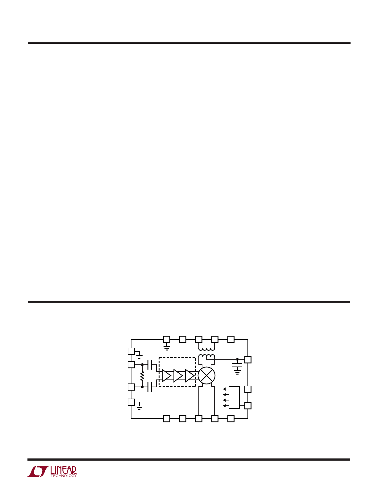
The LT®5520 mixer is designed to meet the high linearity
requirements of wireless and cable infrastructure transmission applications. A high-speed, internally matched,
LO amplifier drives a double-balanced mixer core, allowing the use of a low power, single-ended LO source. An RF
output transformer is integrated, thus eliminating the
need for external matching components at the RF output,
while reducing system cost, component count, board area
and system-level variations. The IF port can be easily
matched to a broad range of frequencies for use in many
different applications.
The LT5520 mixer delivers 15.9dBm typical input 3rd
order intercept point at 1.9GHz with IF input signal levels
of –10dBm. The input 1dB compression point is typically
4dBm. The IC requires only a single 5V supply.
, LTC and LT are registered trademarks of Linear Technology Corporation.
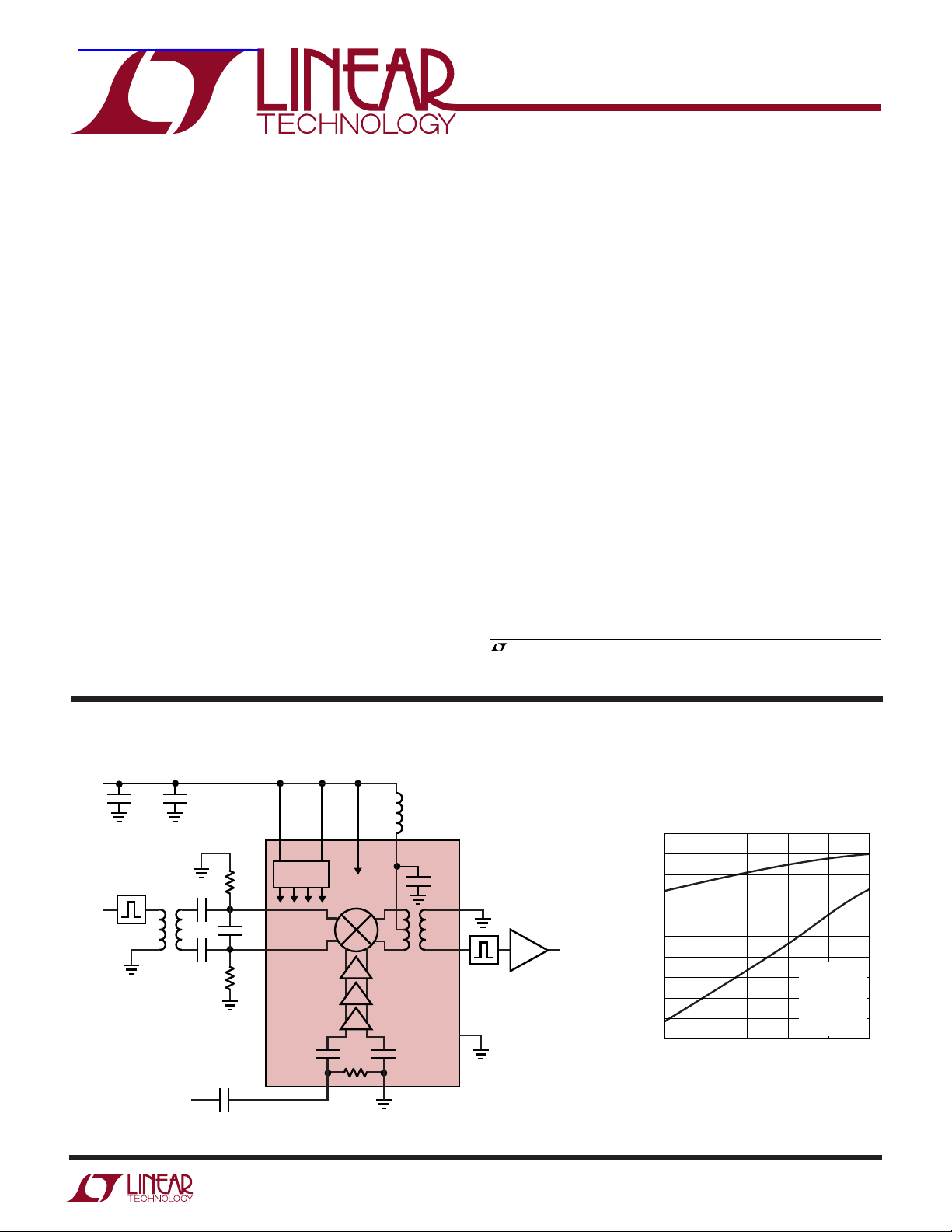
TYPICAL APPLICATIO
5V
DC
1µF 1000pF
EN V
BIAS
+
IF
–
IF
Figure 1. Frequency Conversion in Wireless Infrastructure Transmitter
INPUT
BPF
IF
4:1
LO INPUT
–5dBm
220pF
220pF
100Ω
15pF
100Ω
(OPTIONAL)
U
CC1VCC2VCC3
85Ω
+
LO
RF Output Power and Output IM3 vs
39nH
10pF
+
RF
RF
BPF
PA
OUTPUT
–
RF
GND
5pF5pF
–
LT5520
LO
5520 F01
IF Input Power (Two Input Tones)
10
0
–10
–20
–30
–40
–50
, IM3 (dBm/TONE)
OUT
–60
P
–70
–80
–90
–16
P
OUT
PLO = –5dBm
IM3
–12
–8
IF INPUT POWER (dBm/TONE)
f
f
f
f
T
–4
= 1760MHz
LO
= 140MHz
IF1
= 141MHz
IF2
= 1900MHz
RF
= 25°C
A
0
4
5520 • F01b
5520f
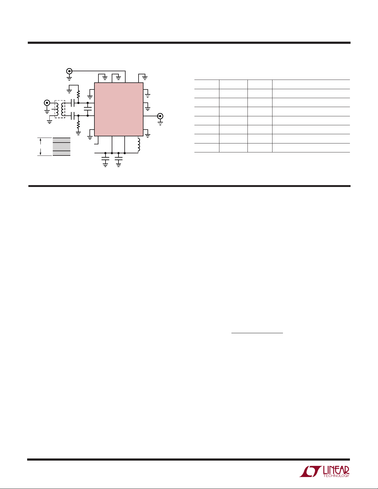
1
LT5520
16 15 14 13
5 6 7 8
TOP VIEW
UF PACKAGE
16-LEAD (4mm × 4mm) PLASTIC QFN
EXPOSED PAD IS GND (PIN 17),
MUST BE SOLDERED TO PCB
9
10
11
12
4
3
2
1
EN
V
CC1VCC2VCC3
GND
IF
+
IF
–
GND
GND
RF
+
RF
–
GND
GND
LO–LO+GND
17
WW
W
ABSOLUTE AXI U RATI GS
U
UUW
PACKAGE/ORDER I FOR ATIO
(Note 1)
Supply Voltage ....................................................... 5.5V
Enable Voltage ............................. –0.3V to (V
+ 0.3V)
CC
LO Input Power (Differential).............................. 10dBm
ORDER PART
NUMBER
LT5520EUF
RF+ to RF– Differential DC Voltage...................... ±0.13V
RF Output DC Common Mode Voltage ......... –1V to V
CC
IF Input Power (Differential) ............................... 10dBm
IF+, IF– DC Currents.............................................. 25mA
LO+ to LO– Differential DC Voltage .......................... ±1V
LO Input DC Common Mode Voltage............ –1V to V
CC
UF PART
MARKING
5520
Operating Temperature Range .................–40°C to 85°C
T
= 125°C, θJA = 37°C/W
Storage Temperature Range ................. –65°C to 125°C
Junction Temperature (TJ)....................................125°C
Consult LTC Marketing for parts specified with wider operating temperature ranges.
JMAX
ELECTRICAL CHARACTERISTICS
PARAMETER CONDITIONS MIN TYP MAX UNITS
IF Input Frequency Range DC to 400 MHz
LO Input Frequency Range 900 to 2700 MHz
RF Output Frequency Range 1300 to 2300 MHz
1900MHz Application: VCC = 5VDC, EN = High, TA = 25°C, IF input = 140MHz at –10dBm, LO input = 1.76GHz at –5dBm, RF output
measured at 1900MHz, unless otherwise noted. Test circuit shown in Figure 2. (Notes 2, 3)
PARAMETER CONDITIONS MIN TYP MAX UNITS
IF Input Return Loss ZO = 50Ω, with External Matching 20 dB
LO Input Return Loss ZO = 50Ω 16 dB
RF Output Return Loss ZO = 50Ω 20 dB
LO Input Power –10 to 0 dBm
Conversion Gain –1 dB
Input 3rd Order Intercept –10dBm/Tone, ∆f = 1MHz 15.9 dBm
Input 2nd Order Intercept –10dBm, Single-Tone 45 dBm
LO to RF Leakage –41 dBm
LO to IF Leakage –35 dBm
Input 1dB Compression 4 dBm
IF Common Mode Voltage Internally Biased 1.77 V
Noise Figure Single Side Band 15 dB
DC ELECTRICAL CHARACTERISTICS
(Test Circuit Shown in Figure 2) VCC = 5VDC, EN = High , TA = 25°C (Note 3), unless otherwise noted.
PARAMETER CONDITIONS MIN TYP MAX UNITS
Enable (EN) Low = Off, High = On
Turn-On Time (Note 4) 2 µs
Turn-Off Time (Note 4) 6 µs
Input Current V
2
DC
ENABLE
= 5V
DC
110 µA
5520f
LT5520
DC ELECTRICAL CHARACTERISTICS
(Test Circuit Shown in Figure 2) VCC = 5VDC, EN = High , TA = 25°C (Note 3), unless otherwise noted.
PARAMETER CONDITIONS MIN TYP MAX UNITS
Enable = High (On) 3V
Enable = Low (Off) 0.5 V
Power Supply Requirements (VCC)
Supply Voltage 4.5 to 5.25 V
Supply Current V
CC
= 5V
DC
60 70 mA
Shutdown Current EN = Low 1 100 µA
DC
DC
DC
Note 1: Absolute Maximum Ratings are those values beyond which the life
of a device may be impaired.
Note 2: External components on the final test circuit are optimized for
operation at f
= 1900MHz, f
RF
= 1.76GHz and f
LO
= 140MHz.
IF
Note 3: Specifications over the –40°C to 85°C temperature range are
assured by design, characterization and correlation with statistical process
controls.
Note 4: Turn-On and Turn-Off times are based on the rise and fall times of
the RF output envelope from full power to –40dBm with an IF input power
of –10dBm.
UW
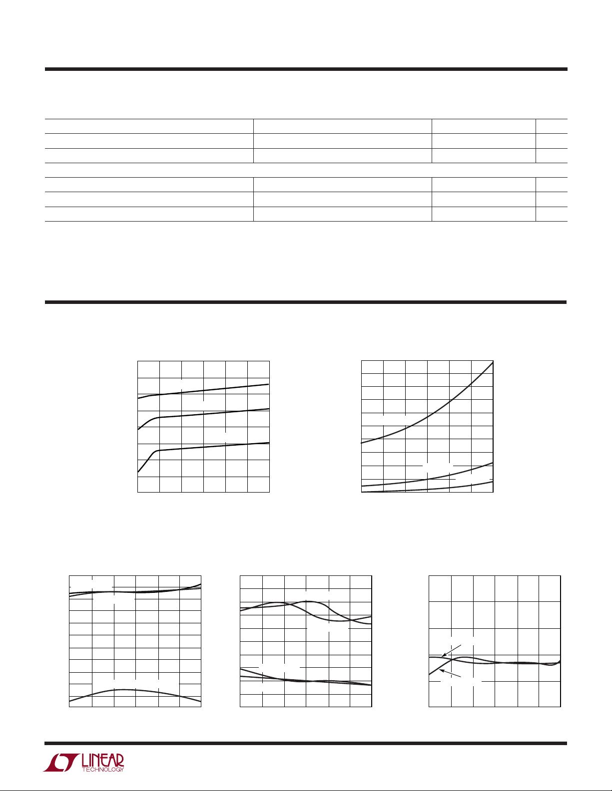
TYPICAL PERFOR A CE CHARACTERISTICS
Supply Current
vs Supply Voltage
66
64
62
60
58
56
SUPPLY CURRENT (mA)
54
52
50
4.0 4.25
TA = 85°C
4.5 5.04.75
SUPPLY VOLTAGE (V)
TA = 25°C
TA = –40°C
5.25
5.5 4.0 4.25 4.5 5.04.75
5520 • GO1
1.0
0.9
0.8
0.7
0.6
0.5
0.4
0.3
SHUTDOWN CURRENT (µA)
0.2
0.1
(Test Circuit Shown in Figure 2)
Shutdown Current
vs Supply Voltage
TA = 85°C
TA = 25°C
TA = –40°C
0
SUPPLY VOLTAGE (V)
5.25
5.5
5520 • GO2
VCC = 5VDC, EN = High, TA = 25°C, IF input = 140MHz at –10dBm, LO input = 1.76GHz at –5dBm, RF output measured at 1900MHz,
unless otherwise noted. For 2-tone inputs: 2nd IF input = 141MHz at –10dBm. (Test Circuit Shown in Figure 2.)
Conversion Gain and SSB Noise
Figure vs RF Output Frequency
18
HIGH SIDE LO
16
14
12
10
8
6
GAIN, NF (dB)
4
2
0
–2
–4
1300 1300
LOW SIDE LO
SSB NF
GAIN
LOW SIDE AND HIGH SIDE LO
1500
RF OUTPUT FREQUENCY (MHz)
1700
1900
23002100
2500
5520 • GO3
IIP3 and IIP2
vs RF Output Frequency
32
30
28
26
24
22
IIP3 (dBm)
20
IIP3
18
16
14
12
LOW SIDE LO
HIGH SIDE LO
1700
1500 2300
RF OUTPUT FREQUENCY (MHz)
LOW SIDE LO
HIGH SIDE LO
2100
1900
IIP2
5520 • GO4
2500
55
50
45
40
35
30
25
20
15
10
5
IIP2 (dBm)
LO-RF Leakage
vs RF Output Frequency
–10
–20
–30
HIGH SIDE LO
–40
LO LEAKAGE (dBm)
–50
LOW SIDE LO
–60
1300 1500 2300
1700
RF OUTPUT FREQUENCY (MHz)
1900
2100
2500
5520 • GO5
5520f
3
LT5520
UW
TYPICAL PERFOR A CE CHARACTERISTICS
VCC = 5VDC, EN = High , TA = 25°C, IF input = 140MHz at –10dBm, LO input = 1.76GHz at –5dBm, RF output measured at 1900MHz,
unless otherwise noted. For 2-tone inputs: 2nd IF Input = 141MHz at –10dBm. (Test Circuit Shown in Figure 2.)
Conversion Gain and SSB Noise
Figure vs LO Input Power
16
14
12
10
GAIN (dB)
–2
–4
8
6
4
2
0
–16
TA = 85°C
TA = 25°C
GAIN
TA = –40°C
TA = 85°C
–12
LO INPUT POWER (dBm)
TA = 25°C
–8
IIP3 and IIP2 vs
LO Input Power
50
45
40
IIP2
35
30
25
IIP3
20
IIP3, IIP2 (dBm)
15
10
5
0
–16
LOW SIDE LO
HIGH SIDE LO
HIGH SIDE LO
LOW SIDE LO
–8
–12
LO INPUT POWER (dBm)
–4
SSB NF
TA = –40°C
5520 • G06
04
5520 • G09
IIP3 and IIP2 vs
LO Input Power
20
18
16
14
NF (dB)
12
10
8
6
4
2
0
40–4
50
TA = 25°C
45
40
35
IIP2
30
25
IIP3
20
IIP3, IIP2 (dBm)
15
10
5
0
–12
–16
TA = 85°C
TA = –40°C
TA = 25°C, TA = –40°C
TA = 85°C
–8
LO INPUT POWER (dBm)
–4
04
5520 • G07
RF Output Power and Output IM3 vs
IF Input Power (Two Input Tones)
10
0
TA = –40°C
–10
–20
P
OUT
–30
–40
–50
, IM3 (dBm/TONE)
P
OUT
–60
–70
–80
–90
TA = –40°C
IM3
–12
–16
IF INPUT POWER (dBm/TONE)
TA = 85°C
–8
TA = 25°C
TA = 85°C
–4
04
5520 • G10
LO-RF Leakage
vs LO Input Power
–10
–20
–30
TA = –40°C
–40
LO LEAKAGE (dBm)
TA = 25°C
–50
–60
–16
–8
–12
LO INPUT POWER (dBm)
–4
RF Output Power and Output IM2 vs
IF Input Power (Two Input Tones)
10
0
–10
–20
–30
–40
, IM2 (dBm/TONE)
–50
OUT
P
–60
–70
–80
TA = –40°C
P
OUT
IM2
TA = 85°C
–12
–16
IF INPUT POWER (dBm/TONE)
TA = 85°C
–8
TA = 25°C
TA = –40°C
–4
TA = 85°C
04
5520 • G08
TA = 25°C
04
5520 • G11
Conversion Gain vs IF Input
Power (One Input Tone)
4
3
2
TA = –40°C
1
0
–1
GAIN (dB)
–2
–3
–4
–5
–6
–16
TA = 25°C
–8
–12
IF INPUT POWER (dBm)
4
TA = 85°C
–4
04
5520 • G12
IF, LO and RF Port Return Loss
vs Frequency
0
–5
–10
–15
RETURN LOSS (dB)
–20
–25
0
LO PORT
IF PORT
500
RF PORT
1000 1500 2000
FREQUENCY (MHz)
2500 3000
5520 • G13
Conversion Gain, IIP3 and IIP2
vs Supply Voltage
8
LOW SIDE LO
7
6
5
4
3
GAIN (dB)
2
1
0
GAIN
–1
–2
4.0 4.25 4.5 5.04.75
HIGH SIDE LO
LOW SIDE LO
LOW SIDE AND HIGH SIDE LO
SUPPLY VOLTAGE (V)
HIGH SIDE LO
5.25
IIP2
IIP3
5520 • G14
50
45
40
35
30
25
20
15
10
5
0
5.5
5520f
IIP3, IIP2 (dBm)
LT5520
U
UU
PI FU CTIO S
GND (Pins 1, 4, 9, 12, 13, 16): Internal Grounds. These
pins are used to improve isolation and are not intended as
DC or RF grounds for the IC. Connect these pins to low
impedance grounds for best performance.
IF+, IF– (Pins 2, 3): Differential IF Signal Inputs. A differential signal must be applied to these pins through DC
blocking capacitors. The pins must be connected to ground
with 100Ω resistors (the grounds must each be capable of
sinking about 18mA). For best LO leakage performance,
these pins should be DC isolated from each other. An
impedance transformation is required to match the IF
input to the desired source impedance (typically 50Ω or
75Ω).
EN (Pin 5): Enable Pin. When the applied voltage is greater
than 3V, the IC is enabled. When the applied voltage is less
than 0.5V, the IC is disabled and the DC current drops to
about 1µA.
V
(Pin 6): Power Supply Pin for the Bias Circuits.
CC1
Typical current consumption is about 2mA. This pin
should be externally connected to VCC and have appropriate RF bypass capacitors.
V
(Pin 7): Power Supply Pin for the LO Buffer Circuits.
CC2
Typical current consumption is about 22mA. This pin
should have appropriate RF bypass capacitors as shown
in Figure 2. The 1000pF capacitor should be located as
close to the pins as possible.
V
(Pin 8): Power Supply Pin for the Internal Mixer.
CC3
Typical current consumption is about 36mA. This pin
should be externally connected to VCC through an inductor. A 39nH inductor is used in Figure 2, though the value
is not critical.
RF–, RF+ (Pins 10, 11): Differential RF Outputs. One pin
may be DC connected to a low impedance ground to realize
a 50Ω single-ended output. No external matching components are required. A DC voltage should not be applied
across these pins, as they are internally connected through
a transformer winding.
LO+, LO– (Pins 14, 15): Differential Local Oscillator Inputs. The LT5520 works well with a single-ended source
driving the LO+ pin and the LO– pin connected to a low
impedance ground. No external matching components are
required. An internal resistor is connected across these
pins; therefore, a DC voltage should not be applied across
the inputs.
GROUND (Pin 17, Exposed Pad): DC and RF ground
return for the entire IC. This must be soldered to the
printed circuit board low impedance ground plane.
BLOCK DIAGRA
W
GND
LO
LO
GND
BACKSIDE
GROUND
17 12 11 10 9
13
5pF
+
14
85Ω
–
15
5pF
16
HIGH SPEED
LO BUFFER
7 1 2 3 4
V
CC2
RF+RF
GND GND
IF
GND
–
8
V
5520 BD
CC3
V
6
CC1
EN
5
5520f
10pF
DOUBLEBALANCED
MIXER
BIAS
+
–
GND
IF
5
LT5520
TEST CIRCUIT
LO
IN
1760MHz
R1
C1
5
C3
4
C2
R2
RF
GND
DC
GND
0.062"
IF
IN
140MHz
0.018"
0.018"
1
2
3
T1
ER = 4.4
16 15 14 13
GND
GND
IF
IF
GND
EN
+
–
LO–LO
LT5520
V
CC1VCC2VCC3
1
2
3
4
EN
V
CC
+
GND
12
GND
11
+
RF
10
–
RF
9
GND
8765
L1
C4C5
5520 TC01
RF
OUT
1900MHz
REF DES VALUE SIZE PART NUMBER
C1, C2 220pF 0402 AVX 04023C221KAT2A
C3 15pF 0402 AVX 04023A150KAT2A
C4 1000pF 0402 AVX 04023A102KAT2A
C5 1µF 0603 Taiyo Yuden LMK107BJ105MA
L1 39nH 0402 Toko LL1005-FH39NJ
R1, R2 100Ω, 0.1% 0603 IRC PFC-W0603R-03-10R1-B
T1 4:1 SM-22 M/A-COM ETC4-1-2
Figure 2. Test Schematic for the LT5520
U
WUU
APPLICATIO S I FOR ATIO
The LT5520 consists of a double-balanced mixer, a highperformance LO buffer, and bias/enable circuits. The RF
and LO ports may be driven differentially; however, they
are intended to be used in single-ended mode by connecting one input of each pair to ground. The IF input ports
must be DC-isolated from the source and driven differentially. The IF input should be impedance-matched for the
desired input frequency. The LO input has an internal
broadband 50Ω match with return loss better than 10dB
at frequencies up to 3000MHz. The RF output band ranges
from 1300MHz to 2300MHz, with an internal RF transformer providing a 50Ω impedance match across the
band. Low side or high side LO injection can be used.
IF Input Port
The IF inputs are connected to the emitters of the doublebalanced mixer transistors, as shown in Figure 3. These
pins are internally biased and an external resistor must be
connected from each IF pin to ground to set the current
through the mixer core. The circuit has been optimized to
work with 100Ω resistors, which will result in approximately 18mA of DC current per side. For best LO leakage
performance, the resistors should be well matched; thus
resistors with 0.1%, tolerance are recommended. If LO
leakage is not a concern, then lesser tolerance resistors
can be used. The symmetry of the layout is also important
for achieving optimum LO isolation.
The capacitors shown in Figure 3, C1 and C2, serve two
purposes. They provide DC isolation between the IF+ and
IF– ports, thus preventing DC interactions that could
cause unpredictable variations in LO leakage. They also
improve the impedance match by canceling excess inductance in the package and transformer. The input capacitor
value required to realize an impedance match at desired
frequency, f, can be estimated as follows:
CC
==
12
2
where; f is in units of Hz, LIN and L
1
2
fL L
π+()( )
IN EXT
EXT
are in H, and C1, C2
are in farad. LIN is the differential input inductance of the
LT5520, and is approximately 1.67nH. L
represents the
EXT
combined inductances of differential external components and transmission lines. For the evaluation board
shown in Figure 10, L
= 4.21nH. Thus, for f = 140MHz,
EXT
the above formula gives C1 = C2 = 220pF.
6
5520f
LT5520
U
WUU
APPLICATIO S I FOR ATIO
100Ω
0.1%
C1
T1
IF
50Ω
IN
4:1
C3
C2
100Ω
0.1%
Figure 3. IF Input with External Matching
Table 1 lists the differential IF input impedance and reflection coefficient for several frequencies. A 4:1 balun can be
used to transform the impedance up to about 50Ω.
Table 1. IF Input Differential Impedance
Frequency Differential Input Differential S11
(MHz) Impedance Mag Angle
10 10.1 + j0.117 0.663 180
44 10.1 + j0.476 0.663 179
70 10.1 + j0.751 0.663 178
140 10.2 + j1.47 0.663 177
170 10.2 + j1.78 0.663 176
240 10.2 + j2.53 0.663 174
360 10.2 + j3.81 0.663 171
500 10.2 + j5.31 0.663 167
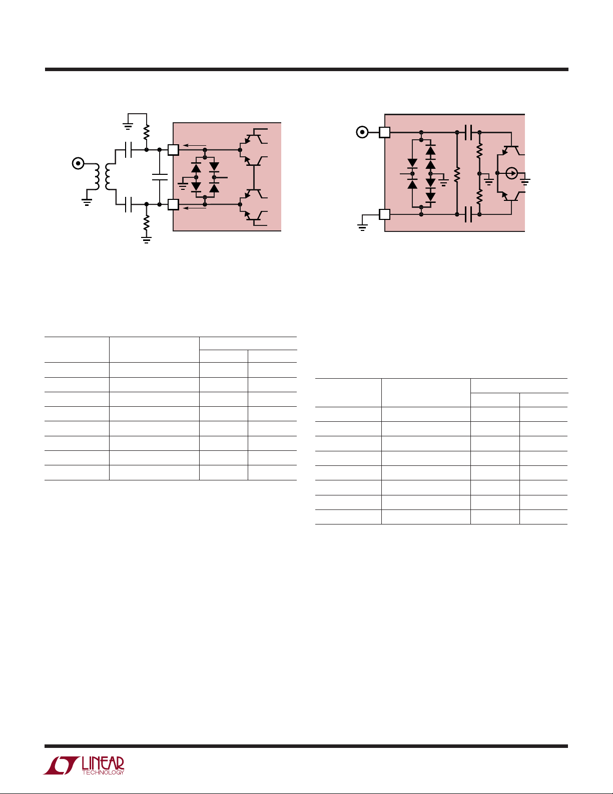
LO Input Port
The simplified circuit for the LO buffer input is shown in
Figure 4. The LO buffer amplifier consists of high-speed
limiting differential amplifiers, optimized to drive the mixer
quad for high linearity. The LO+ and LO– ports can be
driven differentially; however, they are intended to be
driven by a single-ended source. An internal resistor
connected across the LO+ and LO– inputs provides a
broadband 50Ω impedance match. Because of the resistive match, a DC voltage at the LO input is not recommended. If the LO signal source output is not AC coupled,
then a DC blocking capacitor should be used at the LO
input.
2
3
LT5520
18mA
18mA
V
CC
5520 F03
LO
50Ω
+
IN
14
V
15
LO
CC
–
LO
LT5520
5pF
85Ω
5pF
220Ω
220Ω
5520 F04
Figure 4. LO Input Circuit
Though the LO input is internally 50Ω matched, there may
be some cases, particularly at higher frequencies or with
different source impedances, where a further optimized
match is desired. Table 2 includes the single -ended input
impedance and reflection coefficient vs frequency for the
LO input for use in such cases.
Table 2. Single-Ended LO Input Impedance
Frequency Input S11
(MHz) Impedance Mag Angle
1300 62.8 – j9.14 0.139 –30.9
1500 62.2 – j11.4 0.148 –37.1
1700 61.5 – j13.4 0.157 – 42.4
1900 60.0 – j15.2 0.164 – 48.9
2100 58.4 – j16.9 0.172 –54.7
2300 56.5 – j17.9 0.176 –60.4
2500 54.9 – j18.8 0.182 –65.1
2700 53.7 – j18.8 0.182 –68.5
RF Output Port
An internal RF transformer, shown in Figure 5, reduces the
mixer-core impedance to provide an impedance of 50Ω
across the RF+ and RF– pins. The LT5520 is designed and
tested with the outputs configured for single-ended operation, as shown in the Figure 5; however, the outputs can be
used differentially as well. A center-tap in the transformer
provides the DC connection to the mixer core and the
transformer provides DC isolation at the RF output. The
RF+ and RF– pins are connected together through the
secondary windings of the transformer, thus a DC voltage
should not be applied across these pins.
5520f
7

LT5520
U
WUU
APPLICATIO S I FOR ATIO
The impedance data for the RF output, listed in Table 3, can
be used to develop matching networks for different load
impedances.
Table 3. Single-Ended RF Output Impedance
Frequency Input S11
(MHz) Impedance Mag Angle
1300 26.9 + j38.2 0.520 94.7
1500 44.2 + j35.7 0.359 78.4
1700 53.9 + j20.6 0.198 68.0
1900 49.5 + j7.97 0.080 88.9
2100 42.8 + j4.14 0.089 148
2300 38.9 + j5.41 0.139 151
2500 38.7 + j7.78 0.154 140
2700 41.1 – j9.51 0.142 127
+
RF
11
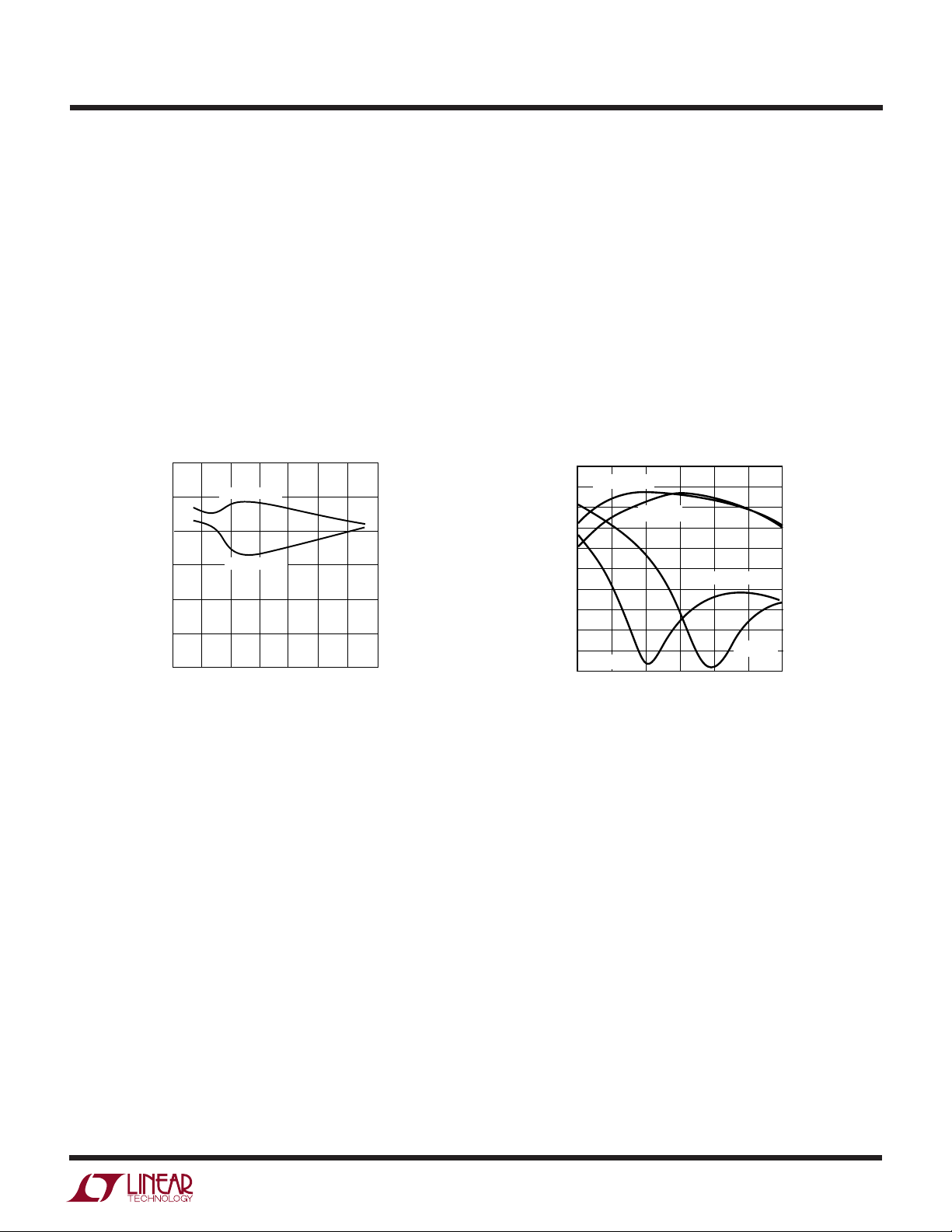
The performance was evaluated with the input tuned for
each of these frequencies and the results are summarized
in Figures 6-8. The same IF input balun transformer was
used for all measurements. In each case, the LO input
frequency was adjusted to maintain an RF output frequency of 1900 MHz.
5
4
IIP3
3
2
1
0
GAIN
GAIN (dB)
–1
–2
–3
–4
–5
0
HIGH SIDE LO
200
100
300
INPUT FREQUENCY (MHz)
LOW SIDE LO
HIGH SIDE LO
LOW SIDE LO
400
500
600
5520 F06
700
20
18
16
14
IIP3 (dBm)
12
10
8
6
4
2
0
V
CC
–
RF
8
V
CC
LT5520
5520 F05
RF
50Ω
OUT
10
Figure 5. RF Output Circuit
Operation at Different Input Frequencies
On the evaluation board shown in Figure 10, the input of
the LT5520 can be easily matched for different frequencies
by changing the input capacitors, C1 and C2. Table 4 lists
some actual values used at selected frequencies.
Table 4. Input Capacitor Values vs Frequency
Frequency Capacitance (C1, C2)
(MHz) (pF)
70 820
140 220
240 68
480 18
650 12
Figure 6. Conversion Gain and IIP3
vs Tuned IF Input Frequency
18
PLO = –5dBm
17
16
NF (dB)
15
14
13
0
HIGH SIDE LO
LOW SIDE LO
200
100
300
INPUT FREQUENCY (MHz)
400
PLO = 0dBm
500
600
700
5520 F07
Figure 7. SSB Noise Figure vs Tuned IF Input Frequency
8
5520f
LT5520
U
WUU
APPLICATIO S I FOR ATIO
Figures 6-8 illustrate the performance versus tuned IF
input frequency with both high side and low side LO
injection. Figure 6 shows the measured conversion gain
and IIP3. The noise figure is plotted in Figure 7 for LO
power levels of –5dBm and 0dBm. At lower input frequencies, the LO power level has little impact on noise figure.
However, for higher frequencies, an increased LO drive
level may be utilized to achieve better noise figure. The
single-tone IIP2 behavior is illustrated in Figure 8.
60
50
40
30
IIP2 (dBm)
20
10
0
0
LOW SIDE LO
HIGH SIDE LO
100 200
300 500
INPUT FREQUENCY (MHz)
400 600 700
5520 F08
Low Frequency Matching of the RF Output Port
Without any external components on the RF output, the
internal transformer of the LT5520 provides a good 50Ω
impedance match for RF frequencies above approximately
1600MHz. At frequencies lower than this, the return loss
drops below 10dB and degrades the conversion gain. The
addition of a single 3.3pF capacitor in series with the RF
output improves the match at lower RF frequencies,
shifting the 10dB return loss point to about 1300MHz, as
demonstrated in Figure 9. This change also results in an
improvement of the conversion gain, as shown in
Figure 9.
OUT
5520 F09
2400
0
–5
–10
–15
–20
–25
RETURN LOSS (dB)
1
0
–1
–2
–3
–4
GAIN (dB)
–5
–6
–7
–8
–9
1200
C
OUT
C
OUT
= 3.3pF
1400
= 3.3pF
NO C
OUT
RETURN LOSS
1800 2000
1600
FREQUENCY (MHz)
GAIN
NO C
2200
Figure 8. IIP2 vs Tuned IF Input Frequency Figure 9. Conversion Gain and Return Loss vs Output Frequency
5520f
9

LT5520
U
WUU
APPLICATIO S I FOR ATIO
(10a) Top Layer Silkscreen (10b) Top Layer Metal
Figure 10. Evaluation Board Layout
10
5520f
PACKAGE DESCRIPTIO
4.35 ± 0.05
2.90 ± 0.05
2.15 ± 0.05
(4 SIDES)
RECOMMENDED SOLDER PAD PITCH AND DIMENSIONS
0.65 BCS
0.72 ±0.05
0.30 ±0.05
U
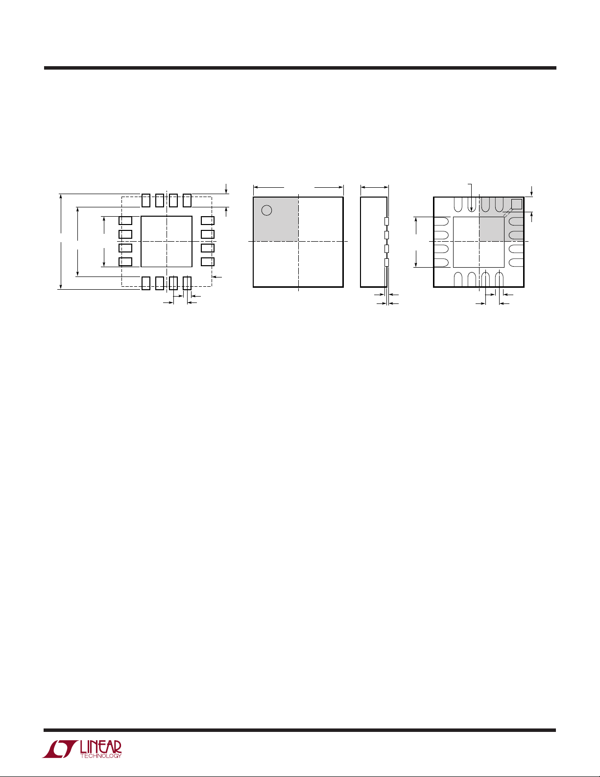
UF Package
16-Lead Plastic QFN (4mm × 4mm)
(Reference LTC DWG # 05-08-1692)
4.00 ± 0.10
(4 SIDES)
PIN 1
TOP MARK
PACKAGE
OUTLINE
NOTE:
1. DRAWING CONFORMS TO JEDEC PACKAGE OUTLINE MO-220 VARIATION (WGGC)
2. ALL DIMENSIONS ARE IN MILLIMETERS
3. DIMENSIONS OF EXPOSED PAD ON BOTTOM OF PACKAGE DO NOT INCLUDE
MOLD FLASH. MOLD FLASH, IF PRESENT, SHALL NOT EXCEED 0.15mm ON ANY SIDE
4. EXPOSED PAD SHALL BE SOLDER PLATED
0.75 ± 0.05
2.15 ± 0.10
(4-SIDES)
0.200 REF
0.00 – 0.05
LT5520
BOTTOM VIEW—EXPOSED PAD
R = 0.115
TYP
1615
0.55 ± 0.20
1
2
(UF) QFN 0802
0.30 ± 0.05
0.65 BSC
Information furnished by Linear Technology Corporation is believed to be accurate and reliable.
However, no responsibility is assumed for its use. Linear Technology Corporation makes no representation that the interconnection of its circuits as described herein will not infringe on existing patent rights.
5520f
11

LT5520
RELATED PARTS
PART NUMBER DESCRIPTION COMMENTS
Infrastructure
LT5511 High Signal Level Upconverting Mixer RF Output to 3GHz, 17dBm IIP3, Integrated LO Buffer
LT5512 DC-3GHz High Signal Level Downconverting Mixer RF Input to 3GHz, 20dBm IIP3, Integrated LO Buffer
LT5515 1.5GHz to 2.5GHz Direct Conversion Quadrature Demodulator 20dBm IIP3,Integrated LO Quadrature Generator
LT5516 0.8GHz to 1.5GHz Direct Conversion Quadrature Demodulator 21.5dBm IIP3,Integrated LO Quadrature Generator
LT5522 600MHz to 2.7GHz High Signal Level Downconverting Mixer 4.5V to 5.25V Supply, 25dBm IIP3 at 900MHz, NF = 12.5dB,
50Ω Single-Ended RF and LO Ports
RF Power Detectors
LT5504 800MHz to 2.7GHz RF Measuring Receiver 80dB Dynamic Range, Temperature Compensated, 2.7V to 6V Supply
LTC5505 RF Power Detectors with >40dB Dynamic Range 300MHz to 3GHz, Temperature Compensated, 2.7V to 5.5V Supply
LTC5507 100kHz to 1000MHz RF Power Detector 300MHz to 3GHz, Temperature Compensated, 2.7V to 5.5V Supply
LTC5508 300MHz to 7GHz RF Power Detector 44dB Dynamic Range, Temperature Compensated, SC70 Package
LTC5509 300MHz to 3GHz RF Power Detector 36dB Dynamic Range, Temperature Compensated, SC70 Package
LTC5532 300MHz to 7GHz Precision RF Power Detector Precision V
RF Receiver Building Blocks
LT5500 1.8GHz to 2.7GHz Receiver Front End 1.8V to 5.25V Supply, Dual-Gain LNA, Mixer LO Buffer
LT5502 400MHz Quadrature IF Demodulator with RSSI 1.8V to 5.25V Supply, 70MHz to 400MHz IF, 84dB Limiting Gain,
90dB RSSI Range
LT5503 1.2GHz to 2.7GHz Direct IQ Modulator and 1.8V to 5.25V Supply, Four-Step RF Power Control,
Upconverting Mixer 120MHz Modulation Bandwidth
LT5506 500MHz Quadrature IF Demodulator with VGA 1.8V to 5.25V Supply, 40MHz to 500MHz IF, –4dB to 57dB
Linear Power Gain, 8.8MHz Baseband Bandwidth
LT5546 500MHz Ouadrature IF Demodulator with 1.8V to 5.25V Supply, 40MHz to 500MHz IF,
VGA and 17MHz Baseband Bandwidth –7dB to 56dB Linear Power Gain
Offset Control, Adjustable Gain and Offset
OUT
12
Linear Technology Corporation
1630 McCarthy Blvd., Milpitas, CA 95035-7417
(408) 432-1900 ● FAX: (408) 434-0507
●
www.linear.com
5520f
LT/TP 1103 1K • PRINTED IN USA
LINEAR TECHNOLOGY CORPORATION 2003
 Loading...