

FEATURES
■
Allows Safe Board Insertion and Removal
from a Live –48V Backplane
■
Circuit Breaker Immunity to Voltage Steps and
Current Spikes
■
Programmable Inrush and
Short-Circuit Current Limits
■
Pin Compatible with LT1640L/LT1640H
■
Operates from –20V to –80V
■
Programmable Overvoltage Protection
■
Programmable Undervoltage Lockout
■
Power Good Control Output
■
Bell-Core Compatible ON/OFF Threshold
U
APPLICATIO S
LT4250L/LT4250H
Negative 48V
Hot Swap Controller
U
DESCRIPTIO
The LT®4250L/LT4250H are 8-pin, negative 48V Hot Swap
controllers that allow a board to be safely inserted and
removed from a live backplane. Inrush current is limited to
a programmable value by controlling the gate voltage of an
external N-channel pass transistor. The pass transistor is
turned off if the input voltage is less than the programmable undervoltage threshold or greater than the overvoltage threshold. A programmable current limit protects
the system against shorts. After a 500µs timeout the
current limit activates the electronic circuit breaker. The
PWRGD (LT4250L) or PWRGD (LT4250H) signal can be
used to directly enable a power module. The LT4250L is
designed for modules with a low enable input and the
LT4250H for modules with a high enable input.
TM
■
Central Office Switching
■
–48V Distributed Power Systems
■
Negative Power Supply Control
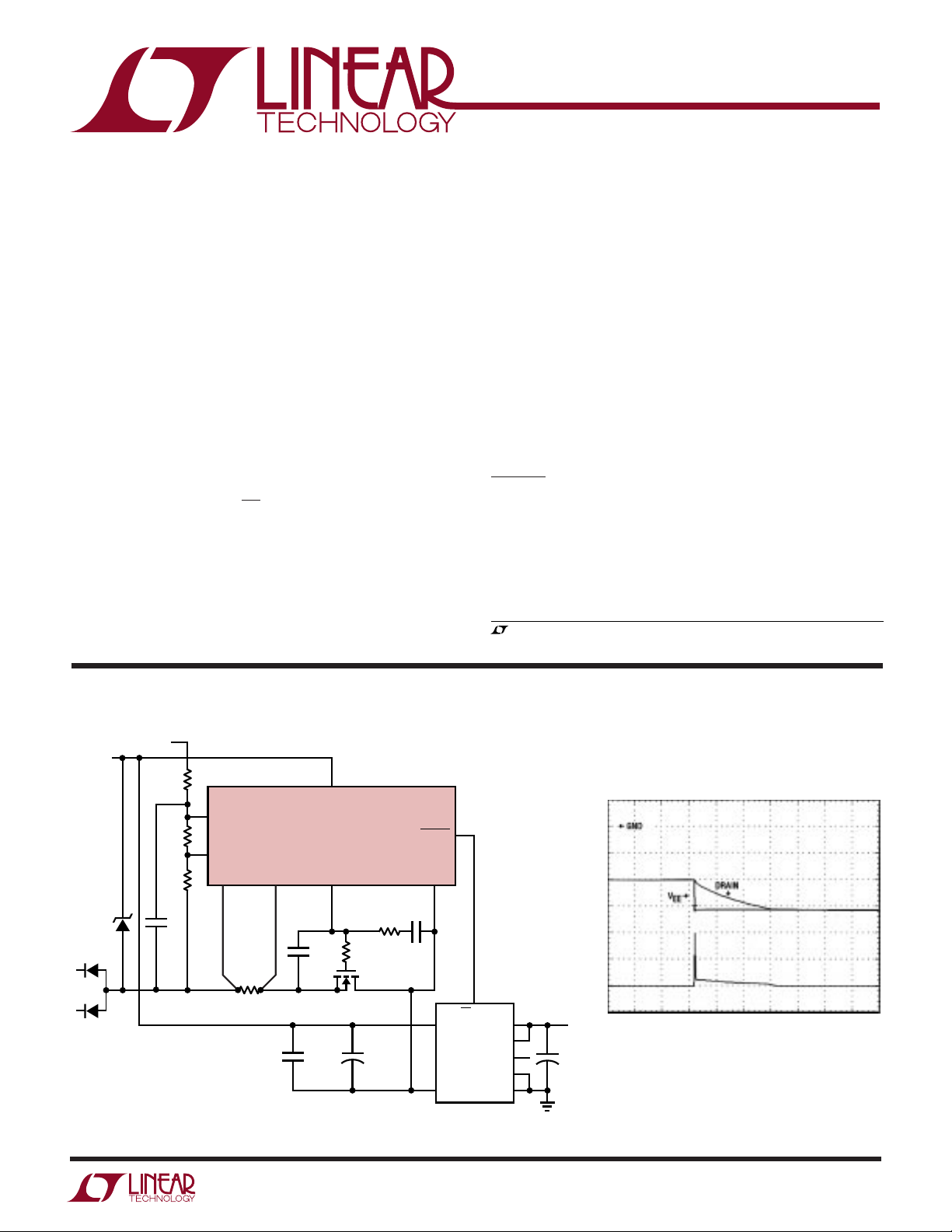
TYPICAL APPLICATIO
–48V RTN
(SHORT PIN)
–48V RTN
UV =
38.5V
UV
RELEASE
AT 43V
OV =
71V
*
–48V
INPUT 1
–48V
INPUT 2
* DIODES INC. SMAT70A
†
THESE COMPONENTS ARE APPLICATION
SPECIFIC AND MUST BE SELECTED BASED
UPON OPERATING CONDITIONS AND DESIRED
PERFORMANCE. SEE APPLICATIONS
INFORMATION.
R4
549k
1%
R5
6.49k
1%
R6
10k
1%
0.1µF
10V
†
3
UV
†
2
OV
†
V
SENSE
EE
4
56
†
R1
0.02Ω
5%
U
8
V
DD
LT4250L
GATE DRAIN
†
R3
1k, 5%
†
R2
C1
10Ω
470nF
5%
25V
Q1
IRF530
C3
0.1µF
100V
C4
+
100µF
100V
C2
15nF
100V
PWRGD
†
1
4
7
+
V
IN
–
V
IN
LUCENT
JW050A1-E
The LT4250L/LT4250H are available in 8-pin PDIP and SO
packages.
, LTC and LT are registered trademarks of Linear Technology Corporation.
Hot Swap is a trademark of Linear Technology Corporation.
Voltage Step On Input Supply
1
VEE AND
DRAIN
20V/DIV
(Q1)
I
D
5A/DIV
2
ON/OFF
V
OUT
SENSE
TRIM
SENSE
V
OUT
9
+
8
+
7
6
–
5
–
5V
C5
+
100µF
16V
4250 TA01
500µs/DIV
4250lhf
1
LT4250L/LT4250H
WW
W
ABSOLUTE MAXIMUM RATINGS
U
(Note 1), All Voltages Referred to V
Supply Voltage (VDD – VEE) .................... –0.3V to 100V
PWRGD, PWRGD Pins ........................... –0.3V to 100V
SENSE, GATE Pins.................................... –0.3V to 20V
UV, OV Pins .............................................. –0.3V to 60V
DRAIN Pin .................................................. –2V to 100V
Maximum Junction Temperature ......................... 125°C
WU
/
PACKAGE
PWRGD
1
OV
2
UV
3
V
4
EE
N8 PACKAGE
8-LEAD PDIP
T
= 125°C, θJA = 120°C/W (N8)
JMAX
T
= 125°C, θJA = 150°C/W (S8)
JMAX
O
RDER I FOR ATIO
TOP VIEW
V
8
DD
DRAIN
7
GATE
6
SENSE
5
S8 PACKAGE
8-LEAD PLASTIC SO
S8 PART MARKING
ORDER PART
NUMBER
LT4250LCN8
LT4250LCS8
LT4250LIN8
LT4250LIS8
4250L
4250LI
EE
Operating Temperature Range
LT4250LC/LT4250HC ............................. 0°C to 70°C
LT4250LI/LT4250HI .......................... – 40°C to 85°C
Storage Temperature Range ................ –65°C to 150°C
Lead Temperature (Soldering, 10 sec)................. 300°C
U
ORDER PART
NUMBER
LT4250HCN8
LT4250HCS8
LT4250HIN8
LT4250HIS8
S8 PART MARKING
4250H
4250HI
PWRGD
OV
UV
V
EE
N8 PACKAGE
8-LEAD PDIP
T
JMAX
T
JMAX
TOP VIEW
1
2
3
4
8-LEAD PLASTIC SO
= 125°C, θJA = 120°C/W (N8)
= 125°C, θJA = 150°C/W (S8)
V
8
DRAIN
7
GATE
6
SENSE
5
S8 PACKAGE
DD
Consult LTC Marketing for parts specified with wider operating temperature ranges.
ELECTRICAL CHARACTERISTICS
The ● denotes the specifications which apply over the full operating
temperature range, otherwise specifications are at TA = 25°C. (Note 2), VDD = 48V, VEE = 0V unless otherwise noted.
SYMBOL PARAMETER CONDITIONS MIN TYP MAX UNITS
DC
V
DD
I
DD
V
UVL
V
CL
I
PU
I
PD
I
SENSE
∆V
V
UVH
V
UVL
V
UVHY
I
INUV
V
OVH
V
OVL
GATE
Supply Voltage Operating Range ● 20 80 V
Supply Current UV = 3V, OV = VEE, SENSE = V
Undervoltage Lockout ● 15.4 V
Current Limit Trip Voltage VCL = (V
GATE Pin Pull-Up Current Gate Drive On, V
GATE Pin Pull-Down Current Gate Drive OFF 24 50 70 mA
SENSE Pin Current V
External Gate Drive (V
UV Pin High Threshold Voltage UV Increasing ● 1.240 1.255 1.270 V
UV Pin Low Threshold Voltage UV Decreasing ● 1.105 1.125 1.145 V
UV Pin Hysteresis 130 mV
UV Pin Input Current VUV = V
OV Pin High Threshold Voltage OV Increasing ● 1.235 1.255 1.275 V
OV Pin Low Threshold Voltage OV Decreasing ● 1.210 1.235 1.255 V
SENSE
GATE
– VEE) ● 40 50 60 mV
SENSE
= V
GATE
= 50mV –20 µA
– VEE), 20V ≤ VDD ≤ 80V ● 10 13.5 18 V
EE
EE
EE
● 1.6 5 mA
● –30 –45 –60 µA
● –0.02 –0.5 µA
2
4250lhf
LT4250L/LT4250H
ELECTRICAL CHARACTERISTICS
The ● denotes the specifications which apply over the full operating
temperature range, otherwise specifications are at TA = 25°C. (Note 2), VDD = 48V, VEE = 0V unless otherwise noted.
SYMBOL PARAMETER CONDITIONS MIN TYP MAX UNITS
V
OVHY
I
INOV
V
DL
V
GH
I
DRAIN
V
OL
I
OH
AC
t
PHLOV
t
PHLUV
t
PLHOV
t
PLHUV
t
PHLSENSE
t
PHLCB
t
PHLDL
t
PHLGH
Note 1: Absolute Maximum Ratings are those values beyond which the life
of a device may be impaired.
OV Pin Hysteresis 20 mV
OV Pin Input Current VOV = V
DRAIN Low Threshold V
GATE High Threshold ∆V
Drain Input Bias Current V
EE
– VEE, DRAIN Decreasing 1.1 1.6 2.3 V
DRAIN
– V
GATE
DRAIN
Decreasing 1.3 V
GATE
= 48V ● 10 80 500 µA
PWRGD Output Low Voltage PWRGD (LT4250L), (V
I
= 1mA ● 0.48 0.8 V
OUT
= 5mA ● 1.2 3.0 V
I
OUT
PWRGD Output Low Voltage PWRGD (LT4250H), V
(PWRGD – DRAIN) I
= 1mA ● 0.75 1.0 V
OUT
Output Leakage PWRGD (LT4250L), V
PWRGD (LT4250H), V
DRAIN
DRAIN
DRAIN
DRAIN
– VEE) < V
= 5V
= 48V, V
= 0V, V
DL
= 80V ● 0.05 10 µA
PWRGD
= 80V ● 0.05 10 µA
PWRGD
● – 0.03 –0.5 µA
OV High to GATE Low Figures 1a, 2 1.7 µs
UV Low to GATE Low Figures 1a, 3 1.5 µs
OV Low to GATE High Figures 1a, 2 5.5 µs
UV High to GATE High Figures 1a, 3 6.5 µs
SENSE High to Gate Low Figures 1a, 4a 1 3 µs
Current Limit to GATE Low Figures 1b, 4b 500 µs
DRAIN Low to PWRGD Low (LT4250L) Figures 1a, 5a 1 µs
DRAIN Low to (PWRGD – DRAIN) High (LT4250H) Figures 1a, 5a 1 µs
GATE High to PWRGD Low (LT4250L) Figures 1a, 5b 1.5 µs
GATE High to (PWRGD – DRAIN) High (LT4250H) Figures 1a, 5b 1.5 µs
Note 2: All currents into device pins are positive; all currents out of device
pins are negative. All voltages are referenced to V
unless otherwise
EE
specified.
UW
TYPICAL PERFOR A CE CHARACTERISTICS
Supply Current vs Supply Voltage
1.8
TA = 25°C
1.7
1.6
1.5
1.4
1.3
SUPPLY CURRENT (mA)
1.2
1.1
0
20 40 80
0
SUPPLY VOLTAGE (V)
60
100
1640 G01
Supply Current vs Temperature
1.6
VDD = 48V
1.5
1.4
1.3
1.2
SUPPLY CURRENT (mA)
1.1
1.0
–50 –25
0255075
TEMPERATURE (°C)
1640 G02
100
Gate Voltage vs Supply Voltage
15
TA = 25°C
14
13
12
11
10
9
GATE VOLTAGE (V)
8
7
6
0
20 60
40
SUPPLY VOLTAGE (V)
100
80
1640 G03
4250lhf
3
LT4250L/LT4250H
TEMPERATURE (°C)
–50
2
OUTPUT IMPEDANCE (kΩ)
3
4
5
6
7
8
–25 2505075
1640 G09
100
V
DRAIN
– VEE > 2.4V
UW
TYPICAL PERFOR A CE CHARACTERISTICS
Gate Voltage vs Temperature
15.0
VDD = 48V
14.5
14.0
13.5
13.0
GATE VOLTAGE (V)
12.5
12.0
–25 0 75
TEMPERATURE (°C)
Gate Pull-Down Current
vs Temperature
55
V
= 2V
GATE
52
49
1640 G04
Current Limit Trip Voltage
vs Temperature
55
54
53
52
51
TRIP VOLTAGE (mV)
50
49
100–50 25 50
48
–50
–25
TEMPERATURE (°C)
50
250
100
75
1640 G05
PWRGD Output Low Voltage
vs Temperature (LT4250L)
0.5
I
= 1mA
OUT
0.4
0.3
Gate Pull-Up Current
vs Temperature
48
V
= 0V
GATE
47
46
45
44
43
42
GATE PULL-UP CURRENT (µA)
41
40
–25 10050250
–50
TEMPERATURE (°C)
PWRGD Output Impedance
vs Temperature (LT4250H)
75
1640 G06
46
43
GATE PULL-DOWN CURRENT (mA)
40
–25 0
–50
25
TEMPERATURE (°C)
50
75
100
1640 G07
0.2
0.1
PWRGD OUTPUT LOW VOLTAGE (V)
0
–25 25050
–50
TEMPERATURE (°C)
75
100
1640 G08
UUU
PIN FUNCTIONS
PWRGD/PWRGD (Pin 1): Power Good Output Pin. This pin
will latch a power good indication when V
of V
and V
EE
connected directly to the enable pin of a power module.
When the DRAIN pin of the LT4250L is above VEE by more
than V
DL
PWRGD pin will be high impedance, allowing the pull-up
is within VGH of ∆V
GATE
or V
is more than VGH from ∆V
GATE
GATE
is within V
DRAIN
. This pin can be
, the
GATE
current of the module’s enable pin to pull the pin high and
turn the module off. When V
V
rises above VGH, the PWRGD pin sinks current to
GATE
VEE, pulling the enable pin low and turning on the module.
drops below V
DRAIN
DL
and
This condition is latched until the GATE pin is turned off via
the UV, OV, UVLO or the electronic circuit breaker.
DL
When the DRAIN pin of the LT4250H is above VEE by more
than VDL or V
is more than VGH from ∆V
GATE
PWRGD pin will sink current to the DRAIN pin which pulls
the module’s enable pin low, forcing it off. When V
drops below VDL and V
rises above VGH, the PWRGD
GATE
sink current is turned off, allowing the module’s pull-up
current to pull the enable pin high and turn on the module.
This condition is latched until the GATE pin is turned off via
the UV, OV, UVLO or the electronic circuit breaker.
GATE
, the
DRAIN
4250lhf
4

UUU
PIN FUNCTIONS
LT4250L/LT4250H
OV (Pin 2): Analog Overvoltage Input. When OV is pulled
above the 1.255V threshold, an overvoltage condition is
detected and the GATE pin will be immediately pulled low.
The GATE pin will remain low until OV drops below the
1.235V threshold.
UV (Pin 3): Analog Undervoltage Input. When UV is
pulled below the 1.125V threshold, an undervoltage
condition is detected and the GATE pin will be immediately pulled low. The GATE pin will remain low until UV
rises above the 1.255 threshold.
The UV pin is also used to reset the electronic circuit
breaker. If the UV pin is cycled low and high following the
trip of the circuit breaker, the circuit breaker is reset and
a normal power-up sequence will occur. The response
time for this pin is 1.5µs. Add an external capacitor to this
pin for additional filtering.
VEE (Pin 4): Negative Supply Voltage Input. Connect to
the lower potential of the power supply.
SENSE (Pin 5): Circuit Breaker Sense Pin. With a sense
resistor placed in the supply path between VEE and
SENSE, the overcurrent condition will pull down the
GATE pin and regulate the voltage across the resistor to
be 50mV. If the overcurrent condition exists for more
than 500µs the electronic circuit breaker will trip and turn
off the external MOSFET.
If the current limit value is set to twice the normal
operating current, only 25mV is dropped across the
sense resistor during normal operation. To disable the
current limit feature, VEE and SENSE can be shorted
together.
GATE (Pin 6): Gate Drive Output for the External
N-Channel MOSFET. The GATE pin will go high when the
following start-up conditions are met: the UV pin is high,
the OV pin is low, (V
is greater than V
UVLOH
– VEE) < 50mV and the VDD pin
SENSE
. The GATE pin is pulled high by a
45µA current source and pulled low with a 50mA current
source. During current limit the GATE pin is pulled low
using a 100mA current source.
DRAIN (Pin 7): Analog Drain Sense Input. Connect this
pin to the drain of the external N-channel MOSFET and the
V– pin of the power module. When the DRAIN pin is
below VDL, the PWRGD/PWRGD pin will latch to indicate
the switch is on.
VDD (Pin 8): Positive Supply Voltage Input. Connect this
pin to the higher potential of the power supply inputs and
the V+ pin of the power module. An undervoltage lockout
circuit disables the chip until the VDD pin is greater than
the 16V V
UVLOH
threshold.
BLOCK DIAGRA
UV
OV
–
+
REF
–
+
W
V
DD
V
GATE
GATE
REF
CC
OUTPUT
DRIVE
+
+
V
DL
–
V
EE
DRAIN
+
–
∆V
–
–
+
GATE
V
4250 BD
GH
PWRGD/PWRGD
4250lhf
UVLO
50mV
–
+
–
+
SENSEV
EE
VCC AND
REFERENCE
GENERATOR
LOGIC
500µs
DELAY
DRIVER
5

LT4250L/LT4250H
2V
1V
4250 F03
t
PHLUV
1.125V
0V
UV
GATE
1V
1.255V
t
PLHUV
PWRGD/PWRGD V
DD
OV
48V
20V
DRAIN
LT4250L/LT4250H
UV GATE
V
EE
SENSE
4250 F01b
V
UV
0.1µF
+
–
+
–
10k
10Ω
10Ω
IRF530
R
5k
+
V
5V
V
OV
V
UV
PWRGD/PWRGD V
OV
LT4250L/LT4250H
UV GATE
V
EE
DRAIN
SENSE
DD
V
DRAIN
V
SENSE
1640 F01a
+
48V
–
Figure 1a. Test Circuit 1
WUW
TIMING DIAGRAMS
OV
GATE
100mV
SENSE
GATE
2V
0V
V
EE
DRAIN
1.255V
t
PHLOV
1V
Figure 2. OV to GATE Timing
60mV
t
PHLSENSE
1V
Figure 4a. SENSE to GATE Timing
1.4V
t
PHLDL
1.235V
Figure 1b. Test Circuit 2
t
PLHOV
1V
4250 F02
Figure 3. UV to GATE Timing
UV
t
PHLCB
GATE
4250 F04a
1V
1V
4250 F04b
Figure 4b. Active Current Limit Timeout
1.4V
∆V
– V
GATE
= 0
t
PHLGH
GATE
GATE
V
EE
PWRGD
DRAIN
PWRGD
V
PWRGD
– V
DRAIN
= 0V
Figure 5a. DRAIN to PWRGD/PWRGD Timing
6
1.4V
t
PHLDL
1V
1V
4250 F05a
V
EE
V
EE
PWRGD
∆V
GATE
PWRGD
V
PWRGD
– V
– V
GATE
DRAIN
1.4V
= 0
GATE
= 0
1V
t
PHLGH
1V
4250 F05b
Figure 5b. GATE to PWRGD/PWRGD Timing
V
EE
4250lhf

LT4250L/LT4250H
U
WUU
APPLICATIONS INFORMATION
Hot Circuit Insertion
When circuit boards are inserted into a live – 48V backplane,
the bypass capacitors at the input of the board’s power
module or switching power supply can draw huge transient currents as they charge up. The transient currents
can cause permanent damage to the board’s components
and cause glitches on the system power supply.
The LT4250 is designed to turn on a board’s supply
voltage in a controlled manner, allowing the board to be
safely inserted or removed from a live backplane. The chip
also provides undervoltage, overvoltage and overcurrent
protection while keeping the power module off until its
input voltage is stable and within tolerance.
Power Supply Ramping
The input to the power module on a board is controlled by
placing an external N-channel pass transistor (Q1) in the
power path (Figure 6a, all waveforms are with respect to
the VEE pin of the LT4250). R1 provides current fault
detection and R2 prevents high frequency oscillations.
Resistors R4, R5 and R6 provide undervoltage and overvoltage sensing. By ramping the gate of Q1 up at a slow
rate, the inrush current charging load capacitors C3 and
C4 can be limited to a safe value when the board makes
connection.
Resistor R3 and capacitor C2 act as a feedback network to
accurately control the inrush current. The C2 capacitor can
be calculated with the following equation:
C2 = (45µA • CL)/I
–48V RTN
(SHORT PIN)
–48V RTN
R4
549k
1%
6.49k
1%
10k
1%
3
R5
2
R6
UV = 38.5V
OV = 71V
*
–48V
* DIODES INC. SMAT70A
INRUSH
C3
8
V
DD
UV
OV
V
EE
4
R1
0.02Ω
5%
LT4250H PWRGD
SENSE
GATE DRAIN
56
C1
470nF
25V
43
21
Q1
IRF530
1k, 5%
R2
10Ω
5%
R3
C2
15nF
100V
0.1µF
100V
C4
+
100µF
100V
1
7
4250 F06a
VICOR
VI-J30-CY
+
V
IN
GATE IN
–
V
IN
+
V
OUT
–
V
OUT
where CL is the total load capacitance = C3 + C4 + module
input capacitance.
Capacitor C1 and resistor R3 prevent Q1 from momentarily turning on when the power pins first make contact.
Without C1 and R3, capacitor C2 would pull the gate of Q1
up to a voltage roughly equal to VEE • C2/C
GS(Q1)
before the
LT4250 could power up and actively pull the gate low. By
placing capacitor C1 in parallel with the gate capacitance
of Q1 and isolating them from C2 using resistor R3 the
problem is solved. The value of C1 is given by:
VV
12=
INMAX TH
C
C1≅ 35 • C2 for V
V
TH
−
CC
•+
()
INMAX
GD
= 72V
where VTH is the MOSFET’s minimum gate threshold and
V
is the maximum operating input voltage.
INMAX
R3 should not exceed a value that produces an
R3 • C2 time-constant of 150µs. A 1k value for R3 will
ensure this for C2 values up to 150nF.
The waveforms are shown in Figure 6b. When the power
pins make contact, they bounce several times. While the
contacts are bouncing, the LT4250 senses an undervoltage
condition and the GATE is immediately pulled low when
the power pins are disconnected.
Once the power pins stop bouncing, the GATE pin starts to
ramp up. When Q1 turns on, the GATE voltage is held
constant by the feedback network of R3 and C2. When the
DRAIN voltage has finished ramping, the GATE pin then
ramps to its final value.
INRUSH
CURRENT
500mA/DIV
5V
GATE –V
+
C5
100µF
16V
10V/DIV
DRAIN
50V/DIV
V
50V/DIV
EE
EE
CONTACT
CONTACT
BOUNCE
BOUNCE
25ms/DIV
MODULE
TURN-ON
MODULE
TURN-ON
4250 F06b
Figure 6a. Inrush Control Circuitry
Figure 6b. Inrush Control Waveforms
4250lhf
7

LT4250L/LT4250H
U
WUU
APPLICATIONS INFORMATION
Current Limit/Electronic Circuit Breaker
The LT4250 features a current limit function that protects
against short circuits or excessive supply currents. If the
current limit is active for more than 500µs the electronic
circuit breaker will trip. By placing a sense resistor
between the VEE and SENSE pin, the current limit will be
activated whenever the voltage across the sense resistor
is greater than 50mV.
Note that the current limit threshold should be set sufficiently high to account for the sum of the load current and
the inrush current. The maximum value of the inrush
current is given by:
I
INRUSH
≤
0840.• –
R
where the 0.8 factor is used as a worst case margin
combined with the minimum trip voltage (40mV).
mV
SENSE
I
LOAD
,
The LT4250 guards against voltage steps on the input
supply. A positive voltage step (increasing in magnitude)
on the input supply causes an inrush current that is
proportional to the voltage slew rate I = CL • ∆V/∆T. If the
inrush exceeds 50mV/R
, the current limit will acti-
SENSE
vate as shown in Figure 8. The GATE pin pulls low, limiting
the current to 50mV/R
. At this level the MOSFET
SENSE
drain will not follow the source as the input voltage rapidly
changes, but instead remains at the voltage stored on the
load capacitance. The load capacitance begins to charge
at a current of 50mV/R
, but not for long. As the load
SENSE
capacitance charges, C2 pushes back on the gate and
limits the MOSFET current in a manner identical to the
initial start-up condition which is less than the short circuit
limiting value of 50mV/R
. Thus the circuit breaker
SENSE
does not trip. To ensure correct operation under input
voltage step conditions, R
must be chosen to pro-
SENSE
vide a current limit value greater than the sum of the load
current and the dynamic current in the load capacitance.
In the case of a short circuit, the current limit circuitry
activates and immediately pulls the GATE low, servos the
SENSE voltage to 50mV, and starts a 500µs timer. The
MOSFET current is limited to 50mV/R
(see Figure 7).
SENSE
If the short circuit persists for more than 500µs, the circuit
breaker trips and pulls the GATE pin low, shutting off the
MOSFET. The circuit breaker is reset by pulling UV low, or
by cycling power to the part. If the short circuit clears
before the 500µs timing interval the current limit will
deactivate and release the GATE.
DRAIN
50V/DIV
GATE
10V/DIV
I
(Q1)
D
5A/DIV
For C2 values less than 10nF a positive voltage step on the
input supply can result in the Q1 turning off momentarily
which can shut down the output. By adding an additional
resistor and diode, Q1 remains on during the voltage step.
This is shown as D1 and R7 in Figure 9. The purpose of D1
is to shunt current around R7 when the power pins first
make contact and allow C1 to hold the GATE low. The value
of R7 should be sized to generate an R7 • C1 time constant
of 33µs.
Under some conditions, a short circuit at the output can
cause the input supply to dip below the UV threshold. The
LT4250 turns off once and then turns on until the electronic circuit breaker is tripped. This can be minimized by
adding a deglitching delay to the UV pin with a capacitor
from UV to VEE. This capacitor forms an RC time constant
with the resistors at UV, allowing the input supply to
recover before the UV pin resets the circuit breaker.
8
1ms/DIV
Figure 7. Short-Circuit Protection Waveforms
4250lhf

LT4250L/LT4250H
V
EE
V
DD
LT4250H
PWRGD
SENSE
C1
150nF
25V
C3
0.1µF
100V
C4
22µF
100V
Q1
IRF530
R2
10Ω
5%
R3
1k
5%
C2
3.3nF
100V
R4
549k
1%
R5
6.49k
1%
R6
10k
1%
R1
0.02Ω
5%
4
3
2
–48V RTN
–48V
OV
UV
56
8
1
GATE DRAIN
4250 F09
+
7
–48V RTN
(SHORT PIN)
*
* DIODES INC. SMAT70A
R7
220Ω
5%
43
21
D1
BAT85
U
WUU
APPLICATIONS INFORMATION
A circuit that automatically resets the circuit breaker after
a current fault is shown in Figure 10. Transistors Q2 and
Q3 along with R7, R8, C4 and D1 form a programmable
one-shot circuit. Before a short occurs, the GATE pin is
pulled high and Q3 is turned on, pulling node 2 to VEE.
Resistor R8 turns off Q2. When a short occurs, the GATE
pin is pulled low and Q3 turns off. Node 2 starts to charge
VEE AND
DRAIN
20V/DIV
(Q1)
I
D
5A/DIV
500µs/DIV
C4 and Q2 turns on, pulling the UV pin low and resetting
the circuit breaker. As soon as C4 is fully charged, R8 turns
off Q2, UV goes high and the GATE starts to ramp up. Q3
turns back on and quickly pulls node 2 back to VEE. Diode
D1 clamps node 3 one diode drop below VEE. The duty
cycle is set to 10% to prevent Q1 from overheating.
Figure 8. Voltage Step on
Input Supply Waveforms
–48V RTN
–48V RTN
Q2
2N2222
*
D1
1N4148
–48V
* DIODES INC. SMAT70A
(SHORT PIN)
549k
R4
R6
549k
1%
1%
R9
10k
1%
16.5k
3
UV
2
OV
R5
1%
1µF
100V
R7
1M
5%
C4
3
ZVN3310
R8
510k
5%
NODE 2
50V/DIV
GATE
2V/DIV
2
Q3
Figure 10. Automatic Restart After Current Fault
Figure 9. Circuit for Input Steps with Small C2 (<10nF)
8
V
DD
C2
15nF
100V
1
C3
+
100µF
100V
7
4250 F10a
V
EE
1s/DIV
4
SENSE
56
R1
0.02Ω
43
5%
21
LT4250L PWRGD
GATE DRAIN
R3
1k, 5%
R2
C1
10Ω
470nF
5%
25V
Q1
IRF530
4250lhf
9

LT4250L/LT4250H
U
WUU
APPLICATIONS INFORMATION
Undervoltage and Overvoltage Detection
The UV (Pin 3) and OV (Pin 2) pins can be used to detect
undervoltage and overvoltage conditions at the power
supply input. The UV and OV pins are internally connected
to analog comparators with 130mV and 20mV of hysteresis respectively. When the UV pin falls below its threshold
or the OV pin rises above its threshold, the GATE pin is
immediately pulled low. The GATE pin will be held low until
UV is high and OV is low.
The undervoltage and overvoltage trip voltages can be
programmed using a three resistor divider as shown in
Figure 11. With R4 = 549k, R5 = 6.49k and R6 = 10K, the
undervoltage threshold is set to 38.5V (with a 43V release
from undervoltage) and the overvoltage threshold is set to
71V. The resistor divider will also gain up the hysteresis
at the UV pin and OV pin to 4.5V and 1.2V at the input
respectively.
PWRGD/PWRGD Output
The PWRGD/PWRGD output can be used to directly enable a power module when the input voltage to the module
is within tolerance. The LT4250L has a PWRGD output for
modules with an active low enable input, and the LT4250H
has a PWRGD output for modules with an active high
enable input.
When the DRAIN voltage of the LT4250H is high with
respect to VEE (Figure 12) or the GATE voltage is low, the
internal transistor Q3 is turned off and I1 and Q2 clamp the
PWRGD pin one SAT drop (≈0.3V) above the DRAIN pin.
Transistor Q2 sinks the module’s pull-up current and the
module turns off.
When the DRAIN voltage drops below VDL and the GATE
voltage is high, Q3 will turn on, shorting the bottom of I
1
to DRAIN and turning Q2 off. The pull-up current in the
module pulls the PWRGD pin high and enables the
module.
When the DRAIN voltage of the LT4250L is high with
respect to VEE or the GATE voltage is low, the internal pulldown transistor Q2 is off and the PWRGD pin is in a high
impedance state (Figure␣ 13). The PWRGD pin will be
pulled high by the module’s internal pull-up current source,
turning the module off. When the DRAIN voltage drops
below VDL and the GATE voltage is high, Q2 will turn on and
the PWRGD pin will pull low, enabling the module.
The PWRGD signal can also be used to turn on an LED or
optoisolator to indicate that the power is good as shown
in Figure 14.
Gate Pin Voltage Regulation
When the supply voltage to the chip is more than 20V, the
GATE pin voltage is regulated at 13.5V above VEE. The gate
voltage will be no greater than 18V for supply voltages up
to 80V.
–48V RTN
4250 F11
VUV = 1.255
VOV = 1.255
–48V RTN
(SHORT PIN)
–48V RTN
R4
R4 + R5+ R6
()
R5 + R6
R4 + R5+ R6
()
R6
–48V
3
R5
2
R6
8
V
DD
UV
LT4250L/LT4250H
OV
V
EE
4
Figure 11. Undervoltage and Overvoltage Sensing
10
–48V RTN
(SHORT PIN)
R4
R5
R6
*
–48V
* DIODES INC. SMAT70A
3
2
V
GATE
C1
DD
I
1
LT4250H
UV
–
+
OV
∆V
GATE
+
GATE
V
GH
–
+
V
DL
+
–
–
V
SENSE
EE
4
56
43
R1
21
Figure 12. Active High Enable Module
ACTIVE HIGH
ENABLE MODULE
+
IN
ON/OFF
–
IN
+
V
OUT
–
V
OUT
4250lhf
8
PWRGD
1
V
+
C3
Q2
Q3
V
EE
R2
Q1
DRAIN
R3
7
C2
V
4250 F12

WUUU
APPLICATIO S I FOR ATIO
LT4250L/LT4250H
–48V RTN
(SHORT PIN)
–48V RTN
LT4250L
R4
3
R5
2
R6
*
–48V
* DIODES INC. SMAT70A
UV
–
+
OV
∆V
GATE
+
GATE
–
V
GH
+
V
DL
+
–
–
V
SENSE
EE
4
R1
21
GATE
56
C1
43
Figure 13. Active Low Enable Module
PACKAGE DESCRIPTIO
ACTIVE LOW
ENABLE MODULE
8
V
DD
PWRGD
1
+
C3
Q2
V
EE
7
DRAIN
R3
C2
R2
Q1
4250 F13
+
V
IN
ON/OFF
–
V
IN
+
V
OUT
–
V
OUT
–48V RTN
(SHORT PIN)
–48V RTN
*
–48V
* DIODES INC. SMAT70A
549k
6.49k
10k
PWRGD
R4
1%
3
UV
R5
2
1%
OV
R6
1%
SENSE
V
EE
4
R1
0.02Ω
5%
21
V
DD
LT4250L PWRGD
GATE DRAIN
Q1
IRF530
R2
10Ω
5%
R3
1k, 5%
C2
15nF
100V
5687
C1
470nF
25V
43
R7
51k
5%
1
MOC207
+
C3
100µF
100V
4250 F14
Figure 14. Using PWRGD to Drive an Optoisolator
U
N8 Package
8-Lead PDIP (Narrow .300 Inch)
(Reference LTC DWG # 05-08-1510)
0.300 – 0.325
(7.620 – 8.255)
0.065
(1.651)
0.009 – 0.015
(0.229 – 0.381)
+0.035
0.325
–0.015
+0.889
8.255
()
–0.381
*THESE DIMENSIONS DO NOT INCLUDE MOLD FLASH OR PROTRUSIONS.
MOLD FLASH OR PROTRUSIONS SHALL NOT EXCEED 0.010 INCH (0.254mm)
TYP
0.045 – 0.065
(1.143 – 1.651)
0.100
(2.54)
BSC
8-Lead Plastic Small Outline (Narrow .150 Inch)
(Reference LTC DWG # 05-08-1610)
0.010 – 0.020
(0.254 – 0.508)
0.008 – 0.010
(0.203 – 0.254)
*
DIMENSION DOES NOT INCLUDE MOLD FLASH. MOLD FLASH
SHALL NOT EXCEED 0.006" (0.152mm) PER SIDE
**
DIMENSION DOES NOT INCLUDE INTERLEAD FLASH. INTERLEAD
FLASH SHALL NOT EXCEED 0.010" (0.254mm) PER SIDE
×
°
45
0.016 – 0.050
(0.406 – 1.270)
0°– 8° TYP
0.053 – 0.069
(1.346 – 1.752)
0.014 – 0.019
(0.355 – 0.483)
TYP
Information furnished by Linear Technology Corporation is believed to be accurate and reliable.
However, no responsibility is assumed for its use. Linear Technology Corporation makes no representation that the interconnection of its circuits as described herein will not infringe on existing patent rights.
(3.302 ± 0.127)
0.018 ± 0.003
(0.457 ± 0.076)
S8 Package
(1.270)
0.130 ± 0.005
0.125
(3.175)
MIN
0.004 – 0.010
(0.101 – 0.254)
0.050
BSC
0.020
(0.508)
MIN
0.255 ± 0.015*
(6.477 ± 0.381)
0.228 – 0.244
(5.791 – 6.197)
0.189 – 0.197*
(4.801 – 5.004)
7
8
1
2
0.400*
(10.160)
MAX
876
1234
5
6
0.150 – 0.157**
(3.810 – 3.988)
3
4
5
N8 1098
SO8 1298
4250lhf
11

LT4250L/LT4250H
TYPICAL APPLICATION
U
Using an EMI Filter Module
Many applications place an EMI filter module in the power
path to prevent switching noise of the module from being
injected back onto the power supply. A typical application
–48V RTN
(SHORT PIN)
–48V RTN
8
V
R4
549k
1%
R5
6.49k
1%
R6
10k
1%
*
–48V
* DIODES INC. SMAT70A
DD
3
UV
LT4250L
2
OV
V
EE
4
R1
0.02Ω
5%
PWRGD
DRAIN
GATE
SENSE
21
1
7
C2
15nF
100V
6
5
43
C1
470nF
25V
Q1
IRF530
R3
1k
5%
R2
10Ω
5%
1N4003
C3
0.1µF
100V
V
V
Figure 15. Typical Application Using a Filter Module
using the Lucent FLTR100V10 filter module is shown in
Figure 15. When using a filter, an optoisolator is required
to prevent common mode transients from destroying the
PWRGD and ON/OFF pins.
R7
51k
5%
LUCENT
C6
0.1µF
100V
1
2
4
JW050A1-E
+
V
IN
ON/OFF
–
V
IN
CASE
V
OUT
SENSE
TRIM
SENSE
V
OUT
3
+
+
–
–
9
8
7
6
5
4250 F15
+
MOC207
+
V
OUT
IN
LUCENT
FLTR100V10
–
V
OUT
IN
CASE
+
C4
0.1µF
100V
–
C5
+
100µF
100V
C7
100µF
16V
5V
RELATED PARTS
PART NUMBER DESCRIPTION COMMENTS
LTC®1421 Dual Hot Swap Controller with Additional –12V Control Operates from 3V to 12V
LTC1422 Hot Swap Controller in SO-8 System Reset Output with Programmable Delay
LT1640AH/LT1640AL –48V Hot Swap Controller in SO-8 LT4250 is a Pin-Compatible Upgrade to LT1640
LT1641-1/LT1641-2 +48V Hot Swap Controller in SO-8 Foldback Current Limit, 9V to 80V, Auto-Retry/Latch-Off
LTC1642 Fault Protected Hot Swap Controller Operates Up to 16.5V, Protected to 33V
LTC1643 PCI Hot Swap Controller 3.3V, 5V, 12V, –12V Supplies for PCI Bus
LTC1645 Dual Hot Swap Controller Operates from 1.2V to 12V, Power Sequencing
LTC1646 Dual CompactPCI Hot Swap Controller 3.3V, 5V Supplies with Precharge and Local PCI Reset Logic
LTC1647 Dual Hot Swap Controller Dual ON Pins for Supplies from 3V to 15V
LTC4211 Hot Swap Controller with Multifunction Current Control 2.5V to 16.5V Supplies, Active Inrush Current Limiting
LTC4251 –48 Hot Swap Controller in SOT-23 Active Current Limiting, Fast Comparator
for Catastrophic Faults
LTC4252 –48 Hot Swap Controller in MSOP Active Current Limiting, Fast Comparator for Catastrophic
Faults, Separate UV/0V Pins, Power-Good Output
4250lhf
LT/TP 0402 2K • PRINTED IN USA
12
Linear Technology Corporation
1630 McCarthy Blvd., Milpitas, CA 95035-7417
(408) 432-1900 ● FAX: (408) 434-0507
●
www.linear-tech.com
LINEAR TECHNOLOGY CORPORATION 2001
 Loading...