

Page 1
FEATURES
■
Hot SwapTM Controller for Positive
and Negative Supplies
■
Supply Tracking Mode
■
±2.7V to ±16.5V Operation
■
Analog Current Limit with Foldback
■
Allows Safe Board Insertion and Removal
from a Live Backplane
■
Open-Collector Power Good Comparators
■
Automatic Retry or Latchoff After a Current Fault
■
Dual Undervoltage Lockout Comparator Inputs
■
Current Fault Indication
U
APPLICATIO S
■
Live Board Insertion
■
RAID Systems
■
–5.2V ECL Supplies
■
Industrial Controls
■
Split Supply Systems
LT4220
Dual Supply
Hot Swap Controller
U
DESCRIPTIO
The LT®4220 16-pin dual voltage Hot Swap controller
allows a board to be safely inserted and removed from a
live backplane. The device operates with any combination
of 2.7V to 16.5V and –2.7V to –16.5V supplies. Using two
external N-channel pass transistors, the board supply
voltages can be ramped up at an adjustable rate. A selectable tracking mode allows dual supply tracking control for
ramping the positive and negative supplies together.
The LT4220 features foldback current limit and latches off
both gates if either supply remains in current limit longer
than an adjustable time period. The IC can be configured
for automatic restart after a delay set by the same timer.
A power good signal indicates when the output voltages
monitored by the two FB comparators are within tolerance,
and the gate drive signals are at their full on voltage.
The LT4220 is available in a 16-lead narrow SSOP
package.
, LTC and LT are registered trademarks of Linear Technology Corporation.
Hot Swap is a trademark of Linear Technology Corporation.
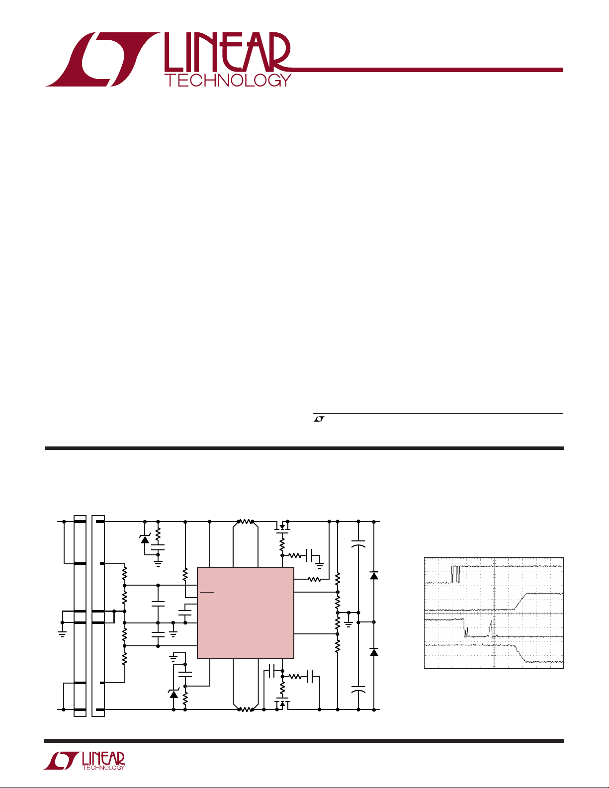
TYPICAL APPLICATIO
±12V 10A Hot Swap Controller
+
12V
V
–12V
V
CC
EE
V
36.5k
4.99k
CONNECTOR 1
CONNECTOR 2
4.99k
36.5k
V
IN
R13
Z1*
R1
R2
R4
R3
–
IN
10Ω
C4
100nF
R15
20k
C7
10nF
10nF
C6
1µF
C8
Z2*
* 1SMA13AT3 TRANSIENT
VOLTAGE SUPPRESSOR
12
11
R14
10Ω
8
9
6
C5
1µF
U
TRACK
+
ON
FAULT
TIMER
GND
–
ON
V
R
S
0.005Ω
716
V
CC
LT4220
EE
SENSEK
12
R
S
0.005Ω
+
SUB85N03-04
R5
10Ω
15 14
+
SENSE
PWRGD
–
SENSE
GATE
34
C3
100nF
–
SUB85N03-04
Q1
GATE
Q2
12V
+
V
OUT
R10
R12
CL1
R9
36.5k
R11
36.5k
CL2
+
–12V
V
OUT
4220 TA01
12V
V
+
IN
12V
+
V
OUT
–12V
–
V
IN
–12V
V
–
OUT
TIME (10ms/DIV)
–
4220f
D1
IN4001
D2
IN4001
+
C1
R6
10nF
1k
+
10
R16, 20k
13
+
FB
4.99k
4.99k
5
–
FB
–
C2
R8
10nF
1k
R7
10Ω
1
Page 2
LT4220
WW
W
U
ABSOLUTE MAXIMUM RATINGS
(Notes 1, 2)
VCC to GND ............................................................. 22V
VEE to GND ........................................................... –22V
TRACK, TIMER .............................. – 0.3V to VCC + 0.3V
ON+, FB+................................. V
ON–, FB–.................................. V
GATE+................................................ –0.3V to VCC + 8V
GATE–..............................–16.5V with VEE = –22V to 0V
SENSE+............................................. –0.3V to VCC + 5V
SENSE–, SENSEK ....................... VEE – 0.3V to V
PWRGD, FAULT ................................. –0.3V to VCC + 5V
Operating Temperature Range
LT4220C...........................................0°C ≤ TA ≤ 70°C
LT4220I ....................................... –40°C ≤ TA ≤ 85°C
Storage Temperature Range ................. –65°C to 150°C
Lead Temperature (Soldering, 10 sec).................. 300°C
– 0.3V to VCC + 0.3V
EE
– 0.3V to V
EE
CC
EE
+ 0.3V
+ 3V
U
W
U
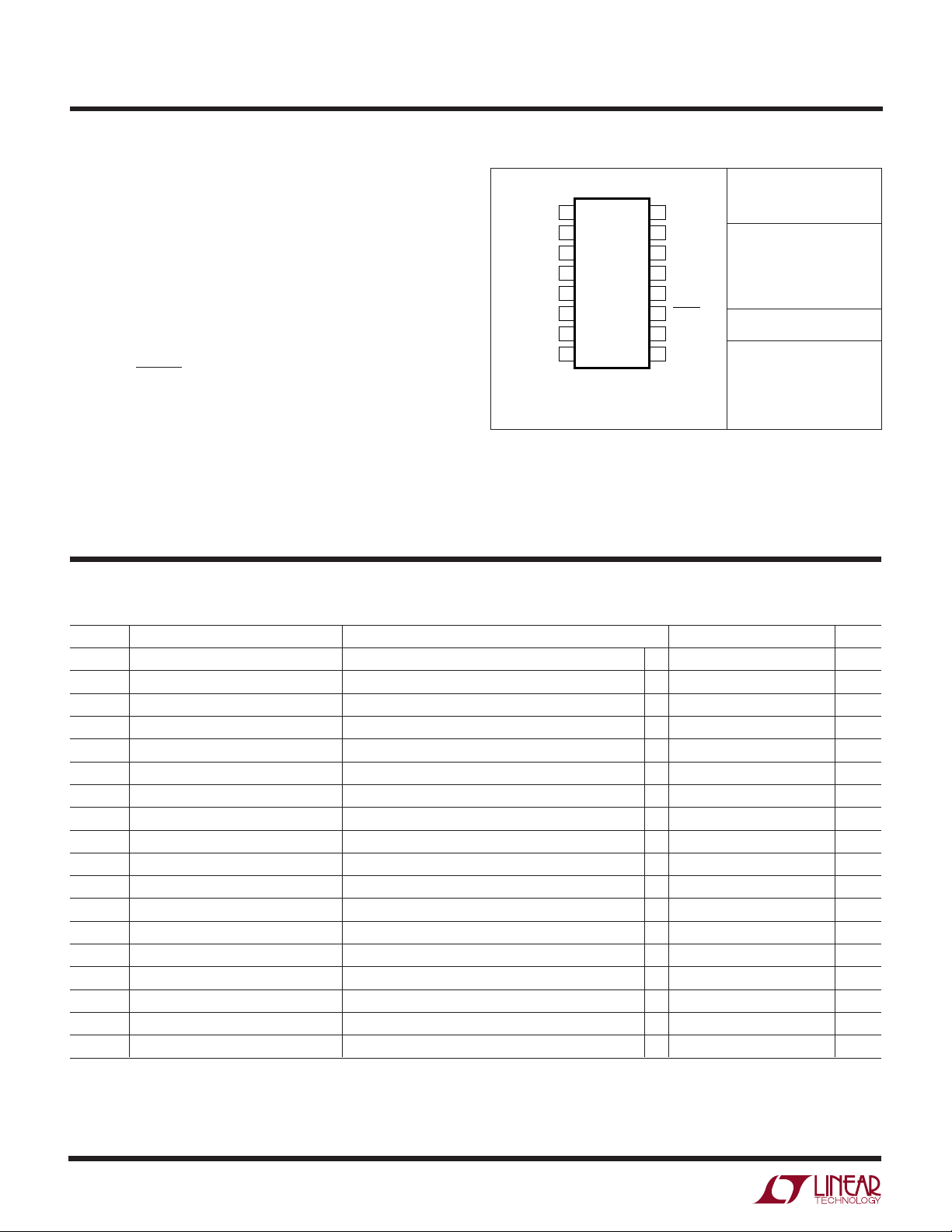
PACKAGE/ORDER INFORMATION
TOP VIEW
1
V
EE
SENSEK
SENSE
Consult LTC Marketing for parts specified with wider operating temperature ranges.
2
–
3
–
4
GATE
–
5
FB
–
6
ON
7
TRACK
8
TIMER
16-LEAD PLASTIC SSOP
T
= 125°C, θJA = 130°C/W
JMAX
GN PACKAGE
16
15
14
13
12
11
10
9
V
CC
SENSE
GATE
+
FB
+
ON
FAULT
PWRGD
GND
+
+
ORDER PART
NUMBER
LT4220CGN
LT4220IGN
GN PART MARKING
4220
4220I
DC ELECTRICAL CHARACTERISTICS
The ● denotes the specifications which apply over the full operating
temperature range, otherwise specifications are at TA = 25°C. VCC = 5V, VEE = –5V, unless otherwise noted.
SYMBOL PARAMETER CONDITIONS MIN TYP MAX UNITS
V
CC
I
CC
V
EE
I
EE
V
PLKO
V
MLKO
V
ON+H
V
ON+HYS
∆V
ON+H
∆V
ON–H
V
ON–HYS
V
ON–H
+
I
ON
–
I
ON
V
FB+H
V
FB+HYS
V
FB–H
V
FB–HYS
VCC Operating Range ● 2.7 16.5 V
VCC Supply Current ● 2.7 4 mA
VEE Operating Range ● –2.7 –16.5 V
VEE Supply Current –1.6 –2.4 mA
VCC Undervoltage Lockout ● 2.35 2.45 2.55 V
VEE Undervoltage Lockout ● –2.4 –2.45 –2.5 V
ON+ ON Threshold ON+ Rising ● 1.22 1.24 1.26 V
ON+ Hysteresis ● 25 50 70 mV
ON+ ON Threshold Line Regulation V
ON– ON Threshold Line Regulation V
ON– Hysteresis ● 25 50 70 mV
ON– ON Voltage Threshold ON– Falling ● –1.22 –1.24 –1.26 V
ON+ Input Current V
ON– Input Current V
FB+ PWRGD Voltage Threshold FB+ Rising ● 1.22 1.24 1.26 V
FB+ Hysteresis Gate = 5V ● 25 50 70 mV
FB– PWRGD Voltage Threshold FB– Falling ● –1.22 –1.24 –1.26 V
FB– Hysteresis Gate = 3V ● 25 50 70 mV
= 2.7V, V
CC
= 2.7V, V
CC
+
= 2V ● 0.01 ±1 µA
ON
–
= GND ● 0.01 ±1 µA
ON
= –2.7V to VCC = 16.5V, VEE = –16.5V ● 0.02 0.15 mV/V
EE
= –2.7V to VCC = 16.5V, VEE = –16.5V ● 0.05 1 mV/V
EE
2
4220f
Page 3
LT4220
DC ELECTRICAL CHARACTERISTICS
The ● denotes the specifications which apply over the full operating
temperature range, otherwise specifications are at TA = 25°C. VCC = 5V, VEE = –5V, unless otherwise noted.
SYMBOL PARAMETER CONDITIONS MIN TYP MAX UNITS
+
I
INFB
I
INFB
∆V
∆
VFB–H
V
SENSE
V
SENSE
I
GATEUP
I
GATEUP
I
GATEDN
I
GATEDN
∆V
∆V
V
TIMERH
V
TIMERL
I
TIMERUP
I
TIMERDN
I
TIMER(R)
V
OL
I
OH
V
FOL
I
FPH
V
TRKTHR
I
TRK
V
TRKFB
V
TRKFB
FB+ Input Current FB+ = 3V ● 0.09 ±1 µA
–
FB– Input Current FB– = –3V ● 0.08 ±1 µA
FB+ PWRGD Threshold Line Regulation V
FB+H
FB– PWRGD Threshold Line Regulation V
+
SENSE+ Trip Voltage (VCC – V
–
SENSE– Trip Voltage (V
+
GATE+ Pull-Up Current Charge Pump On, V
–
GATE– Pull-Up Current V
+
GATE+ Pull-Down Current Any Fault Condition, V
–
GATE– Pull-Down Current Any Fault Condition, V
+
External N-Channel GATE+ Drive V
GATE
–
External N-Channel GATE– Drive V
GATE
SENSEK
+
)V
SENSE
– V
SENSE
= 2.7V, V
CC
= 2.7V, V
CC
+
= 0V, GATE+ – 0.5V ● 61522 mV
FB
+
V
= 1V, GATE+ – 0.5V 36 48 60 mV
FB
–
–
)V
= 0V, GATE– – 0.5V ● –10 –15 –22 mV
FB
–
= –1V, GATE– – 0.5V –43 –52 –61 mV
V
FB
– = –3V ● –6 –10 –14 µA
GATE
+
– VCC, VCC = 2.7V, VEE = –2.7V ● 3.5 4 6 V
GATE
= 5V to 16.5V, VEE = –5V to –16.5V 5 6.5 8 V
V
CC
–
– VEE, VCC = 2.7V, VEE = –2.7V ● 3.5 5.2 6 V
GATE
= 5V to 16.5V, VEE = –5V to –16.5V 7.5 8.5 9 V
V
CC
= –2.7V to VCC = 16.5V, VEE = –16.5V ● 0.015 0.15 mV/V
EE
= –2.7V to VCC = 16.5V, VEE = –16.5V ● 0.05 0.5 mV/V
EE
+
= 7V ● –9 –13 –17 µA
GATE
+
= 1V ● 20 40 60 mA
GATE
–
= VEE + 4V ● 30 70 130 mA
GATE
TIMER High Threshold, Sets FAULT ● 1.22 1.24 1.26 V
TIMER Low Threshold, Allows Restart ● 0.4 0.5 0.6 V
TIMER Pull-Up Current TIMER = 0V ● –40 –65 –85 µA
TIMER Pull-Down Current TIMER = 1V ● 2 3.3 4.5 µA
TIMER Current Ratio I
TIMERDN/ITIMERUP
57 %
PWRGD Output Low Voltage IO = 2mA ● 0.3 V
= 5mA 0.5 V
I
O
PWRGD Leakage Current V
= 16.5V ● 0.1 2 µA
PWRGD
FAULT Output Low Voltage IO = 2mA ● 0.3 V
= 5mA 0.5 V
I
O
FAULT Leakage Current V
= 16.5V ● 0.06 2 µA
FAULT
TRACK Input Threshold ● 0.3 0.8 1.1 V
TRACK Input Current TRACK = 16.5V ● 0.05 2 µA
+
TRACK Mode FB+ Threshold I
–
TRACK Mode FB– Threshold I
+
= 0µA, TRACK = V
GATE
–
= 0µA, TRACK = V
GATE
(Note 3) ● 40 70 mV
CC
(Note 3) ● 40 80 mV
CC
4220f
3
Page 4
LT4220
AC ELECTRICAL CHARACTERISTICS
The ● denotes the specifications which apply over the full operating
temperature range, otherwise specifications are at TA = 25°C. VCC = 5V, VEE = –5V, unless otherwise noted.
SYMBOL PARAMETER CONDITIONS MIN TYP MAX UNITS
+
t
PHLON
t
PLHON
t
PHLFB
t
PLHFB
t
PHLON
t
PLHON
t
PHLFB
t
PLHFB
t
SENSE
t
SENSE
Note 1: Absolute Maximum Ratings are those values beyond which the life
of a device may be impaired.
Note 2: All currents into device pins are positive; all currents out of device
ON+ Low to GATE+ Low 5k Pull-Up to GATE+, 1nF Load Capacitor ● 0.6 0.8 1.2 µs
+
ON+ High to GATE+ High 5k Pull-Up to GATE+, 1nF Load Capacitor ● 0.6 1.5 3 µs
+
FB+ Low to PWRGD Low 5k Pull-Up to PWRGD ● 0.5 0.8 1.2 µs
+
FB+ High to PWRGD High 5k Pull-Up to PWRGD ● 0.6 1.25 3 µs
–
ON– Low to GATE– Low 5k Pull-Up to GATE–, 1nF Load Capacitor ● 0.6 1 1.5 µs
–
ON– High to GATE– High 5k Pull-Up to GATE–, 1nF Load Capacitor ● 1 2.1 3.5 µs
–
FB– Low to PWRGD Low 5k Pull-Up to PWRGD ● 0.6 1 1.5 µs
–
FB– High to PWRGD High 5k Pull-Up to PWRGD ● 0.8 1.25 2 µs
+
SENSE+ to GATE+ Low 1nF On GATE+, 100mV Step, 5k Pull-Up ● 146 µs
–
SENSE– to GATE– Low 1nF On GATE–, 100mV Step, 5k Pull-Up ● 146 µs
pins are negative. All voltages referenced to ground (GND) unless
specified.
+
Note 3: The absolute voltage difference between FB
force either the GATE
+
or GATE– current to 0µA.
and FB– required to
UW
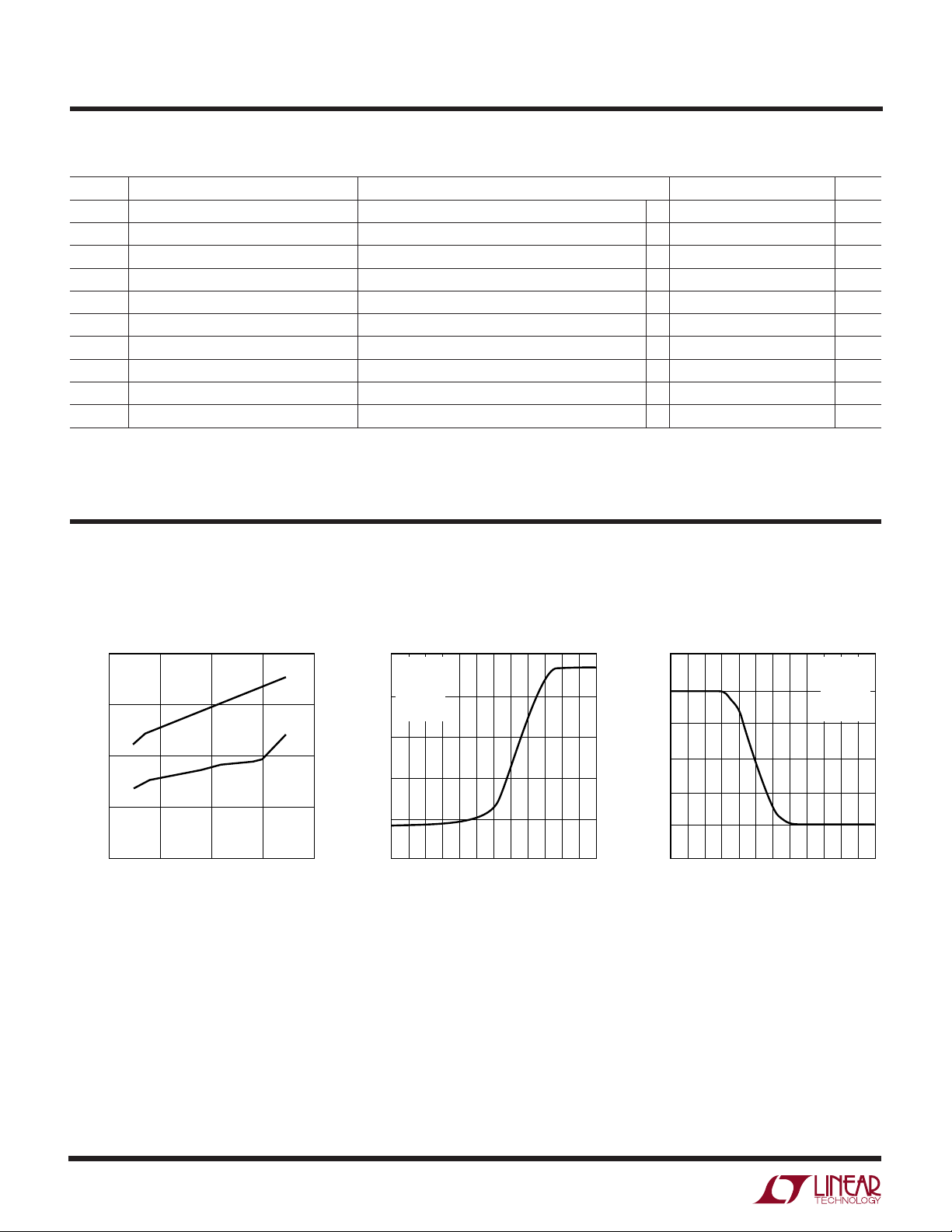
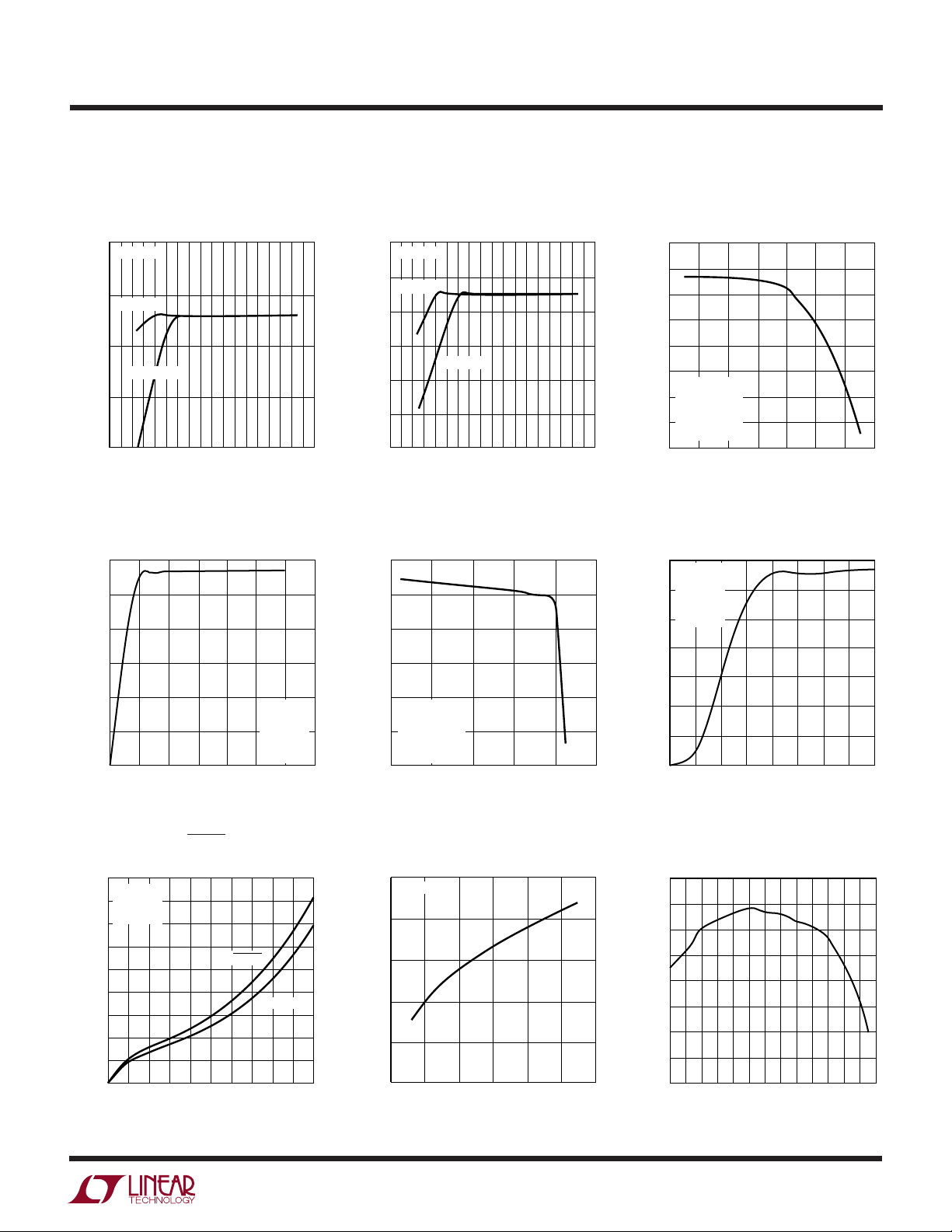
TYPICAL PERFOR A CE CHARACTERISTICS
Supply Current vs Supply Voltage
4
TA = 25°C
I
CC
3
2
I
EE
SUPPLY CURRENT (mA)
1
0
0
5
10
SUPPLY VOLTAGE (V)
Positive Circuit Breaker Sense
Voltage vs FB+ Voltage
50
VCC = 5V
= –5V
V
EE
+
= 2V
ON
40
–
= –2V
ON
= 25°C
T
A
30
VOLTAGE (mV)
+
20
-SENSE
CC
V
10
0
15
20
4220 G01
–1.5
–0.5 0 0.5
–1.0
FB+ VOLTAGE (V)
1.0 1.5 –1.5
4220 G02
Negative Circuit Breaker Sense
Voltage vs FB– Voltage
60
50
40
VOLTAGE (mV)
–
30
20
SENSEK-SENSE
10
0
–0.5 0 0.5 1.0 1.5
–1.0
–
VOLTAGE (V)
FB
VCC = 5V
= –5V
V
EE
+
= 2V
ON
–
= –2V
ON
= 25°C
T
A
4220 G03
4
4220f
Page 5
UW
TYPICAL PERFOR A CE CHARACTERISTICS
GATE+ Drive vs V
8
TA = 25°C
) (V)
7
CC
VEE = –5V
– V
+
GATE
6
DRIVE (V
+
GATE
VEE = –2.7V
5
4
CC
3069121518
VCC (V)
4220 G04
GATE– Drive vs V
10
TA = 25°C
9
VCC = 5V
) (V)
EE
8
– V
–
GATE
7
6
DRIVE (V
–
GATE
5
4
EE
VCC = 2.7V
3069121518
VEE (V)
4220 G05
GATE+ Pull-Up Current vs
GATE+ Voltage
16
14
12
10
8
6
PULL-UP CURRENT (µA)
VCC = 5V
+
GATE
= –5V
V
4
EE
+
= V
V
2
0
0
SENSE
V
SENSE
TA = 25°C
CC
–
= V
EE
24
1357
GATE+ VOLTAGE (V
LT4220
6
+
– VCC) (V)
GATE
4220 G06
GATE+ Pull-Down Current vs
GATE+ Voltage
60
50
40
30
20
PULL-DOWN CURRENT (mA)
+
10
GATE
0
0
48
2 6 10 14
GATE
+
VOLTAGE (V)
PWRGD and FAULT VOL vs
Sink Current
900
VCC = 5V
800
= –5V
V
EE
= 25°C
T
A
700
600
500
(mV)
OL
400
V
300
200
100
0
02
4
SINK CURRENT (mA)
VCC = 5V
= –5V
V
EE
+
ON
= 0V
+
= 2V
FB
= 25°C
T
A
12
4220 G07
FAULT
PWRGD
6810
4220 G10
GATE– Pull-Up Current vs
GATE– Voltage
12
10
8
6
4
PULL-UP CURRENT (µA)
–
VCC = 5V
= –5V
V
EE
SENSE
SENSE– = V
TA = 25°C
0
GATE
+
= V
CC
EE
48
2106
–
VOLTAGE (V
GATE
2
0
TIMER Pull-Up Current vs V
75
TA = 25°C
70
65
60
55
TIMER PULL-UP CURRENT (µA)
50
3069121518
VCC (V)
GATE
–
– VEE) (V)
CC
4220 G08
4220 G11
GATE– Pull-Down Current vs
GATE– Voltage
70
VCC = 5V
= –5V
V
EE
–
60
= 0V
ON
–
= –2V
FB
50
T
= 25°C
A
40
30
20
PULL-DOWN CURRENT (mA)
–
10
GATE
0
0
1
GATE
3658
24
–
VOLTAGE (V
ON+, ON– and FB+, FB
Hysteresis vs Temperature
45.0
44.5
44.0
43.5
43.0
42.5
42.0
HYSTERESIS VOLTAGE (mV)
41.5
41.0
–40
–20 0
20 60
TEMPERATURE (°C)
–
– VEE) (V)
GATE
–
40 80
7
4220 G09
4220 G12
4220f
5
Page 6

LT4220
UW
TYPICAL PERFOR A CE CHARACTERISTICS
FB+ and ON+ Threshold Voltage vs
Temperature
1.241
1.240
1.239
1.238
1.237
THRESHOLD VOLTAGE (V)
1.236
1.235
–40
–20 0
TEMPERATURE (°C)
40 80
20 60
4220 G13
FB– and ON– Threshold Voltage vs
Temperature
–1.241
–1.240
–1.239
–1.238
–1.237
THRESHOLD VOLTAGE (V)
–1.236
–1.235
–40 20 60
–20 0
TEMPERATURE (°C)
GATE+, GATE– Pull-Up Current vs
Temperature
15
+
GATE
14
13
40 80
4220 G14
TIMER Pull-Up Current vs
Temperature
70
69
68
67
66
TIMER PULL-UP CURRENT (µA)
65
64
–40 20 60
–20 0
TEMPERATURE (°C)
40 80
4220 G15
12
PULL-UP CURRENT (µA)
–
, GATE
+
11
GATE
10
–40 20 60
–20 0
TEMPERATURE (°C)
–
GATE
40 80
4220 G16
6
4220f
Page 7

LT4220
U
UU
PI FU CTIO S
VEE (Pin 1): Negative Supply. The negative supply input
ranges from –2.7V to –16.5V for normal operation. IEE is
typically –1.6mA. An internal undervoltage lockout circuit
disables the device for inputs greater than –2.45V. A 10Ω,
1µF RC bypass network from V
transients from the device.
SENSEK (Pin 2): Negative Supply Current Limit Kelvin
Sense Pin. Connect to V
IN
SENSE– (Pin 3): Negative Supply Current Limit Sense Pin.
A sense resistor is placed in the supply path between
SENSEK and SENSE–. The current limit circuit will regulate
the voltage across the sense resistor to
–50mV (SENSEK – SENSE–) when the FB– voltage is less
than –0.7V. If V
–
goes above –0.7V, the voltage across
FB
the sense resistor decreases linearly and stops at –15mV
when V
–
is 0V. If current limit is not used, connect to
FB
SENSEK.
GATE– (Pin 4): Gate Drive for the External Negative Supply
N-Channel FET. An internal 10µA current source drives the
pin. An external capacitor connected from the GATE– pin
to V
– will control the rising slope of the V
OUT
The voltage is clamped to 9V above VEE.
When the current limit is reached, the GATE– pin voltage
will be adjusted to maintain a constant voltage across the
–
R
resistor while the timer capacitor starts to charge. If
S
the TIMER pin voltage exceeds 1.24V, the fault latch will be
set and both GATE– and GATE+ pins will be pulled low.
The GATE– pin is pulled to VEE whenever the ON+ pin is
below 1.24V, the ON– pin is above –1.24V, or either supply
is in the undervoltage lockout voltage range, or the fault
latch is set by the TIMER pin rising above 1.24V.
FB– (Pin 5): Negative Power Good Comparator Input. This
pin monitors the negative output voltage (V
external resistive divider. When the voltage on FB– is
below –1.24V and the initial GATE– drive voltage has
reached a maximum (indicated by setting the internal
GATE– good latch) and the FB+ release conditions are met,
the PWRGD pin is released. PWRGD is pulled low when the
FB– pin is above –1.185V. Note the PWRGD pin is wireORed with the FB+ pin conditions.
–.
– to the V
IN
pin decouples
EE
– signal.
OUT
–) with an
OUT
FB– also controls the negative supply current limit sense
amplifier input offset to provide foldback current limit. The
FB– pin linearly reduces the negative supply sense amplifier offset from –52mV to –15mV for FB– in the range
–0.75V < FB– < 0V. To disable VEE PWRGD and foldback
current limit, the FB– pin should be set to a voltage in the
range: –1.3V > FB– > VEE + 0.5V but should never be more
negative then –5.8V for normal operation.
ON– (Pin 6): The Negative Supply Good Comparator Input.
This pin monitors the negative input voltage (VEE) with an
external resistive divider for undervoltage lockout. When
the voltage at the ON– pin is below the V
high-to-low
ON–H
threshold (–1.24V), the negative supply is considered
good. If the ON– pin rises above –1.185V, both GATE– and
GATE+ are pulled low. If ON– is not used, the ON– pin
should be set to –1.3V > ON– > VEE + 0.5V.
TRACK (Pin 7): Supply Tracking Mode Control. If the TRACK
pin is pulled high, the internal supply tracking circuit will
be enabled during start-up. The TRACK circuit monitors
the FB+ and the FB– pins to keep their magnitude within a
small voltage range by controlling the GATE+ and GATE
–
charge currents. The tracking is disabled when either FB
comparator indicates the output is good. Tracking is reenabled if ON+ is pulled below 1.185V, ON– is pulled above
–1.185V or either supply is below the internal undervoltage
lockout. Typically, the TRACK pin is tied to GND or to VCC.
If left floating, tracking is enabled.
TIMER (Pin 8): Fault Time Out Control. An external timing
capacitor at this pin programs the maximum time the part
is allowed to remain in current limit before issuing a fault
and turning off the external FETs. Additionally, for
autorestart, this pin controls the time before an autorestart
is initiated.
When the part goes into current limit, a 65µA pull-up
current source starts to charge the timing capacitor. When
the voltage reaches V
TIMERH
(1.24V), the internal fault
latch is set, FAULT pulls low and both GATE pins are pulled
low; the pull-up current will be turned off and the capacitor
is discharged by a 3.3µA pull-down current. When the
TIMER pin falls below 0.5V, the part is allowed to restart
if the ON+ pin is pulsed below 1.185V, thereby resetting
internal fault latch—typically done by connecting the
4220f
7
Page 8

LT4220
U
UU
PI FU CTIO S
FAULT pin to the ON+ pin, otherwise the part remains
latched off.
To disable the timeout circuit breaker, connect the TIMER
pin to GND.
GND (Pin 9): Supply Ground Pin.
PWRGD (Pin 10): Open-Collector Output to GND. PWRGD
goes to high impedance after the initial GATE– and final
GATE+ pins have reached their maximum voltage and after
the FB+ pin goes above 1.24V low-to-high threshold and
after the FB– pin falls below –1.24V high-to-low threshold.
An external pull-up resistor can pull the pin to a voltage
higher or lower than VCC. If not used, PWRGD can be left
floating or tied to GND.
FAULT (Pin 11): Open-Collector Output to GND. The
FAULT pin is pulled low whenever the TIMER pin rises
above V
TIMERH
internal fault latch. It goes to high impedance whenever the
internal fault latch is reset. The fault latch is reset with
either internal undervoltage lockout conditions, or by the
ON comparators if the TIMER pin is also below 0.5V. If not
used, the FAULT pin can be left floating or tied to GND.
ON+ (Pin 12): Positive Supply Good Comparator Input. It
monitors the positive input voltage (VCC) with an external
resistive divider for undervoltage lockout. When the voltage on ON+ is above the V
(1.24V) the positive supply is considered good. If ON
drops below 1.185V, both GATE– and GATE+ are pulled
low.
If ON+ is pulled low after a current limit fault and when the
TIMER pin is below 0.5V, the fault latch is reset allowing
the part to turn back on. Typically the FAULT pin is tied
back to the ON+ pin for autorestart. If not used, the ON+ pin
should be set to a voltage in the range of 1.3V < ON+ < V
+ 0.3V. The ON+ pin requires a bypass capacitor connected
to ground.
FB+ (Pin 13): Positive Power Good Comparator Input. This
pin monitors the positive output voltage (V
external resistor divider. When the voltage on FB+ is above
the V
FB+H
drive voltage has reached a maximum, the PWRGD is
(1.24V) threshold, thereby setting the
high-to-low threshold
ON+H
+) with an
OUT
low-to-high threshold (1.24V) and the GATE
+
CC
+
released. PWRGD is pulled low when the FB+ pin is below
1.185V. The PWRGD pin is wire-ORed with the FB– pin
conditions.
FB+ also controls the positive current limit sense amplifier
input offset to provide foldback current limit. The FB+ pin
linearly reduces the positive sense amplifier offset from
48mV to 15mV for FB+ in the range 0.85V > FB+ > 0V. If
PWRGD and foldback current limit are not used, the FB
+
pin should be set to a voltage in the range of 1.3V < FB+ <
VCC + 0.3V.
GATE+ (Pin 14): High Side Gate Drive for the External
Positive Supply N-Channel FET. An internal charge pump
guarantees at least 3.5V above VCC, for supply voltages at
±2.7V increasing to a minimum of 5V above VCC for supply
voltages greater than ±5V. A 10µA pull-up current source
drives the pin. An external capacitor connected from the
GATE+ pin to GND will control the rising slope of the GATE
+
signal. The voltage is clamped to 7V above VCC.
When the current limit is reached, the GATE+ pin voltage
will be adjusted to maintain a constant voltage across the
+
R
resistor while the timer capacitor starts to charge. If
S
the TIMER pin voltage exceeds 1.24V, the GATE+ pin will
be pulled low.
The GATE+ pin is pulled to GND whenever the ON+ pin is
below 1.24V, the ON– pin is above –1.24V, either supply is
in the undervoltage lockout voltage range, or the TIMER
pin rises above 1.24V.
SENSE+ (Pin 15): Positive Supply Current Limit Sense Pin.
A sense resistor must be placed in the supply path between V
and SENSE+. The current limit circuit will
CC
regulate the voltage across the sense resistor to 50mV
(V
– SENSE+) when the FB+ voltage is greater than
CC
0.85V. If V
+
goes below 0.85V, the voltage across the
FB
sense resistor decreases linearly and stops at 15mV when
+
V
is 0V.
FB
VCC (Pin 16): Positive Supply. The positive supply input
ranges from 2.7V to 16.5V for normal operation. ICC is
typically 2.7mA. An internal undervoltage lockout circuit
disables the chip for inputs less than 2.45V. Place a 0.1µF
bypass capacitor next to the VCC pin.
8
4220f
Page 9

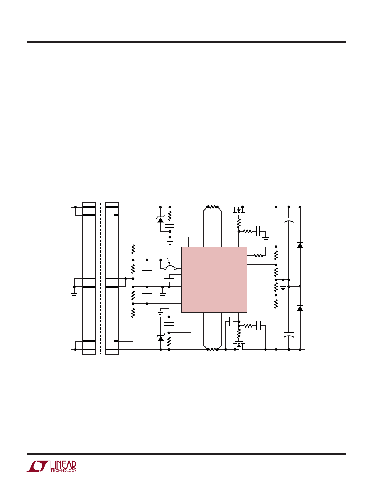
BLOCK DIAGRA
1.24V
W
+
–
+
TIMER AND LOGIC
S
Q
R
R
Q
FAULT
LATCH
FAULT
CURRENT LIMIT
FROM SENSE AMPS
I
LIM
FAULT
11
LT4220
V
CC
60µA
TIMER
8
3µA
ON
12
ON
6
FB
13
FB
5
TRACK
7
0.5V
1.24V
+
+
–
–
+
–1.24V
1.24V
+
–
+
–
P GATE
GOOD
–
+
–1.24V
–
–
ON
PUMP
V
V
CC
EE
UVLO
AND
GOOD
GATE ON
10µA
+
V
CC
–
+
FB
+
–
53mV
+
GATE
14
+
SENSE
15
+
TRACK
–
EN
V
CC
ON
10µA
–
GATE
+
4
SRQ
Q
GATE GOOD
LATCHES
10
PWRGD
–
N GATE
GOOD
SRQ
Q
SRQ
Q
TRACK OFF
LATCH
TOFF
4220 BD
SUBSTRATE
+
52mV
WEAK DIODES
V
1
EE
–
GND
9 16
V
2
3
CC
SENSEK
SENSE
V
CC
–
4220f
9
Page 10
LT4220
WUW
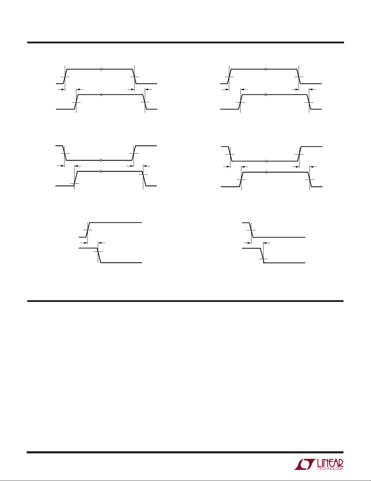
TI I G DIAGRA S
ON
GATE
ON
GATE
V
+
0V
+
0V
1V 1V
+
t
PLHON
0.5V
10V
100mV
t
4220 F01
PHLON
+
FB
PWRGD
+
0V
0V
1V 1V
+
t
PLHFB
2.5V
Figure 1. ON+-to-GATE+ Timing Figure 2. FB+-to-PWRGD Timing
0V
–
–
EE
–1V
t
PLHON
VEE + 1.2V
–1V
–
VEE + 3.5V
t
PHLON
4220 F03
–
FB
PWRGD
0V
–
0V
–1V
t
2.5V
PLHFB
–
Figure 3. ON–-to-GATE– Timing Figure 4. FB–-to-PWRGD Timing
VCC – SENSE
GATE
100mV
+
0V
+
50mV
t
SENSE
10V
VEE – SENSE
+
0V
4220 F05
GATE
0V
–
–
–50mV
t
–2V
SENSE
100mV
+
t
PHLFB
2.5V
4220 F02
–1V
–
t
PHLFB
2.5V
4220 F04
4220 F06
–100mV
V
EE
–
Figure 5. SENSE+-to-GATE+ Timing
WUUU
APPLICATIO S I FOR ATIO
Hot Circuit Insertion
When circuit boards are inserted into a live backplane, the
circuit board bypass capacitors can draw large peak
currents from the backplane power bus as they charge up.
The LT4220 is designed to turn on a board’s ±V dual
supplies in a controlled manner, allowing the circuit board
to be safely inserted or removed from a live backplane. The
part provides supply tracking as well as undervoltage and
overcurrent protection. Power good and fault output signals indicate, respectively, if both power output voltages
are ready or if an overcurrent time-out fault has occurred.
Figure 6. SENSE–-to-GATE– Timing
The dual power supply on the circuit board is controlled
with two external N-channel pass transistors Q1 and Q2 in
the ±V dual power supply path. The sense resistors R
and R
C2 control the V
– provide current detection while capacitor C1 and
S
OUT
+ and V
– slew rate. Optionally, the
OUT
+
S
TRACK pin can be tied to VCC enabling the dual output
voltages to ramp up together by tracking the voltages at
the FB+ and FB– pins. Resistors R6 and R8 provide current
control loop compensation while R5 and R7 prevent high
frequency oscillations in Q1 and Q2. C3 and R8 on Q2
prevent fast dV/dt transients from turning Q2 on during
4220f
10
Page 11
WUUU
APPLICATIO S I FOR ATIO
LT4220
live insertion. Resistive dividers R1, R2 and R3, R4 provide undervoltage sensing. Resistor dividers R9, R10 and
R11, R12 provide a power good signal and control output
voltage tracking when TRACK is enabled.
Internal Supply Diodes
The LT4220 contains two internal diodes which clamp V
EE
and VCC with respect to GND in the event either supply pin
is floating. VEE is clamped one diode above GND and V
CC
is clamped one diode below GND. The current through
these diodes are designed to handle 10mA internal device
current and should not be used for high load current
conditions.
BACKPLANE
CONNECTOR
V
CC
ESD
CONTROL
V
EE
GND MUST CONNECT FIRST
STAGGERED
PCB EDGE
CONNECTOR
GND
+
V
IN
R13
1µF
10Ω
C4
100nF
12
11
C5
1µF
R14
10Ω
8
9
6
C6
Z1*
R1
R2
R4
R3
–
V
IN
*TRANSIENT VOLTAGE SUPPRESSOR
C7
C8
CONNECT FOR
AUTO RESTART
Z2*
TRACK
FAULT
TIMER
GND
ON
Initial Power-Up Sequence
After the power pins first make contact, transistors Q1 and
Q2 remain off. If the voltage at the ON+ and ON– pins
exceed the turn-on threshold voltage, the internal voltage
on the VCC and VEE power pins exceed the undervoltage
lockout threshold, and the timer pin voltage is less than
1.24V, the gate drive to transistors Q1 and Q2 will be
turned on. The voltage on the GATE+ and GATE– pins will
be regulated to control the inrush current if the voltage
across R
+
S
or R
–
exceeds the sense amplifier current
S
limit threshold. If supply tracking is enabled, each gate will
also be regulated to keep the magnitudes at the FB+ and
FB– pins within 50mV of each other.
+
R
ON
7
16 15 14
V
CC
+
–
V
EE
SENSEK
S
LT4220
R
S
SENSE
SENSE
–
R5
10Ω
+
PWRGD
–
C3
100nF
Q1
GATE
GATE
Q2
FB
FB
4321
R7
10Ω
+
V
OUT
C1
R6
10nF
1k
+
10
R16, 20k
13
+
R10
R12
5
–
C2
10nF
R11
–
R8
1k
+
CL1
D1
IN4001
R9
D2
IN4001
+
CL2
V
–
OUT
4220 F07
Figure 7. Hot Swap Controller on Daughter Board with Tracking Disabled
4220f
11
Page 12
LT4220
WUUU
APPLICATIO S I FOR ATIO
Whenever the output voltages reach their final value as
sensed by R9, R10 and R11, R12 and both gate signals are
fully on, the PWRGD pin will go high impedance.
A typical timing sequence is shown in Figure 8 with
tracking enabled. The sequence is as follows:
1) The power pins make contact and the undervoltage
lockout thresholds are exceeded.
2) The ON comparator thresholds are exceeded and the
GATE pins start ramping up. V
+ follows GATE+ by
OUT
the N-channel FET threshold voltage.
3) GATE+ is limited by the tracking circuit because V
lags behind V
+. When V
OUT
– starts ramping, GATE
OUT
OUT
–
–
holds at approximately the threshold voltage of the
N-channel FET due to C2 slew rate control.
4) When the magnitude of V
GATE+ resumes ramping. The slowest V
the faster V
slew rate.
OUT
– catches up with V
OUT
will limit
OUT
OUT
+,
5) GATE+ internal gate good signal threshold is reached.
6) GATE– internal gate good signal threshold is reached,
enabling the FB output comparators. If both FB com-
12 3 4 5 6
V
GATE
CC
V
EE
+
ON
–
ON
+
+UVLO
–UVLO
parators indicate the output is good, the PWRGD pin
output goes high impedance and is pulled up by an
external pullup resistor.
Power Supply Ramping
For large capacitive loads, the inrush current will be limited
by the V
OUT
+ and V
– slew rate or by the fold-back
OUT
current limit. For a desired inrush current that is less than
the fold-back current limit, the feedback networks R6, C1
and R8, C2 can be used to control the V
slew rate. For
OUT
the desired inrush current and typical gate pull-up current,
the feedback network capacitors C1 and C2 can be calculated as:
C1 = (10µA • CL1)/I
C2 = (10µA • CL2)/I
+ and (1)
INRUSH
– (2)
INRUSH
where CL1 and CL2 are the positive and negative output
load capacitance. If the supply-tracking mode is enabled
(TRACK = High), during startup, the output with the
slowest slew rate will also limit the slew rate of the
opposite output (Note: Supply-tracking is also controlled
by the resistive dividers on the FB pins. See Supply
Tracking). Additionally, C1 and C2 should be greater than
5nF to prevent large overshoot in the output voltage for
transient loads with small capacitive loads.
Capacitor C3 and resistor R8 prevent Q2 from momentarily turning on when the power pins first make contact.
Without C3, capacitor C2 and C
would hold the gate
GD(Q2)
of Q2 near ground before the LT4220 could power up and
pull the gate low. The minimum required value of C3 can
be calculated by:
12
V
+
OUT
–
GATE
V
–
OUT
PWRGD
Figure 8. Typical Timing Sequence
4220 F08
VV
−
EE TH
C
3212
=
V
TH
CC
()•.
()
GD Q
2
+
(3)
where VTH is the MOSFET’s minimum gate threshold and
V
is the maximum negative supply input voltage. If
EEMAX
C2 is not used, the minimum value for C3 should be 10nF
to ensure stability. C2 and C3 must be the same type to
ensure tracking over temperature.
4220f
Page 13

WUUU
APPLICATIO S I FOR ATIO
LT4220
Current Limit/Electronic Circuit Breaker
The LT4220 features foldback current limit with an electronic circuit breaker that protects against short-circuits
or excessive supply currents. The current limit is set by
placing sense resistors between VCC (Pin 16) and SENSE
+
(Pin 15) and between SENSEK (Pin 2) and SENSE– (Pin 3).
An adjustable timer will trip an electronic circuit breaker if
the part remains in current limit for too long.
To prevent excessive power dissipation in the pass transistors and to prevent voltage spikes on the input supply
during overcurrent conditions at the output, the current
folds back as a function of the output voltage, which is
sensed at the feedback pins FB+ and FB– . When the voltage
at the FB+ (or FB–) pin is 0V, the sense amplifier offset is
15mV (–15mV), and limits the current to I
+
R
(–15mV/R
S
–
). As the output voltage increases, the
S
LIMIT
= 15mV/
sense amplifier offset increases until the FB+ (or FB–)
voltage reaches 0.85V (–0.75V), At which point the current limit reaches a maximum of I
(–52mV/R
–
).
S
LIMIT
= 48mV/R
+
S
Timer Function and Autorestart
The TIMER pin (Pin 8) provides a method for setting the
maximum time the LT4220 is allowed to operate in current
limit. When the current limit circuitry is not active, the
TIMER pin is pulled to GND by a 3.3µA current sink.
Whenever the current limit circuit becomes active, by
either a positive or negative sense amplifier operating in
current limit, a 65µA pull-up current source is connected
to the TIMER pin and the voltage rises with a slope equal
to dV/dt = 65µA/C
. The desired current limit time (t)
TIMER
can be set with a capacitor value of:
C
= t • 65µA/1.24V (4)
TIMER
If the current limit circuit turns off, the TIMER pin will be
discharged to GND at a rate of:
dV/dt = 3.3µA/C
TIMER
(5)
Whenever the TIMER pin ramps up and reaches the 1.24V
threshold, the internal fault latch is set and the FAULT pin
(Pin 11) is pulled low. GATE+ is pulled down to ground,
GATE– is pulled down to VEE, and the TIMER pin starts
ramping back to GND by the 3.3µA current sink. After the
fault latch is set, the LT4220 can be restarted by pulling the
ON+ pin low after the TIMER pin falls below 0.5V. The
LT4220 can also be restarted by cycling either supply
beyond its UVLO. Otherwise the part remains latched off.
For autorestart, the FAULT pin can be tied to the ON+ pin.
The autorestart will occur after the TIMER pin falls below
0.5V.
Undervoltage Detection
The ON+ and ON– pins can be used to detect an undervoltage
condition at the power supply inputs. The ON+ and ON
–
pins are connected to analog comparators with 50mV of
hysteresis. If the ON+ pin falls below its threshold voltage
or the ON– pin rises above its threshold voltage, the GATE
pins are pulled low and held low until the ON+ and ON– pins
exceed their turn-on thresholds (1.24V and –1.24V). External capacitance at the ON pins may be required to filter
supply ringing from crossing the ON comparator threshold.
Additionally there is an internal undervoltage lockout on
both supplies of approximately VCC < 2.45V and VEE >
–2.45V. If either supply is in UVLO, both GATE pins will be
pulled low and all internal latches will be reset.
ON– Protection
If the ON– pin is driven directly and not connected to the
negative supply through a resistor divider, a 10k resistor
must be connected between the driver and the ON– pin.
Power Good Detection
The LT4220 includes two comparators for monitoring the
output voltages. The FB+ and the FB– pins are compared
against 1.24V and –1.24V internal references respectively.
The comparators exhibit 50mV of hysteresis. The comparator outputs are wire-ORed to the open collector PWRGD
pin that is enabled once both GATE+ and GATE– pins have
reached their maximum gate drive voltage as indicated by
the internal gate good latches. The PWRGD pin goes high
impedance when both FB+ and FB– inputs exceed V
and V
thresholds, GATE+ is fully on and Gate– initially
FB–H
FB+H
has been fully on.
4220f
13
Page 14

LT4220
WUUU
APPLICATIO S I FOR ATIO
Supply Tracking
If the TRACK pin (Pin 7) is high the supply power-up
tracking mode is enabled. This feature forces both supplies to reach their final value at the same time, during
power-up and for faults that drive the output supplies to
zero. During this mode the GATE pins are controlled to
keep the differential magnitude of the FB pins to within
50mV. The FB pins are scaled versions of the output
voltages. Therefore, control of the FB pins, via the GATE
pins, will control the output voltages at the same scale.
|∆V
FB(TRK)
| = |V
FB
+
–
– V
| (6)
FB
Supply tracking will continue until: either FB pin reaches
the associated PWRGD threshold. If any fault condition
occurs that turns the GATE pins off, supply tracking will be
reenabled. The GATE off conditions include: (1) either ON
pin detects undervoltage, (2) internal undervoltage lockout, (3) the fault latch is set by a current limit time-out.
VEE Bypassing
The VEE supply pin should be filtered with an RC network
to reduce high dV/dt slew rates from disturbing internal
circuits. Typical RC bypassing sufficient to prevent circuit
misbehavior is R14 = 10Ω and C5 = 1µF. The GATE–,
SENSEK and SENSE– pins have been designed such that
they can be pulled below or above VEE for short periods of
time while the VEE pin is reaching its steady state voltage.
If desired, a higher R14 • C5 time constant may be used to
prevent short circuit transients from tripping the V
EE
undervoltage lockout circuit at –2.45V. R14 should be
sufficient to decouple C5 from causing transients on V
IN–
during live insertion.
Under the condition of a short circuit on V
inductance and resistance in the V
– path will cause VIN–
IN
–, parasitic
OUT
to collapse toward 0V causing the VEE pin voltage to also
discharge toward 0V before the external FET can be turned
off (typically 7µs to 10µs). To prevent a UVLO condition
from occurring, the R14 • C5 time constant should be
sufficient to hold the VEE pin voltage out of the VEE UVLO
voltage range. If the VEE pin reaches its UVLO voltage,
GATE+ will also be pulled low. For the case where C3 is
large, causing an even slower N-channel FET turnoff,
higher RC bypassing may be necessary to prevent tripping
the VEE UVLO.
ON+, ON– Bypass Capacitors
Bypass capacitors are required from ON+ to ground and
ON– to ground. A typical time constant is:
TC (ON+) = (R1||R2)C7 = 44µs
TC (ON–) = (R3||R4)C8 = 44µs
Supply Ringing
Normal circuit design practice calls for capacitive bypassing of the input supply to active devices. The opposite is
true for Hot Swap circuits that are connected into a
backplane, where capacitive loading would cause transients during an abrupt connection to the backplane. With
little or no capacitive decoupling on the powered side of
the N-channel FETs, connection transients or load transients will typically cause ringing on the supply leads due
to parasitic inductance. It is recommended to use a
snubber circuit comprising of a series 10Ω and 0.1µF
capacitor to dampen transient ringing. The supply
decoupling circuit on the VEE pin also provides a snubber
for V
–.
IN
Additionally, if the supply voltage overshoot can exceed
the ±22V maximum rating on the part, a transient voltage
suppressor is recommended. Voltage transients can occur during load short-circuit conditions, where parasitic
inductance in the supply leads can build up energy before
the external N-channel FET can be turned off. This is
especially true for the negative side FET where a large C3
value slows the turn off of the N-channel FET. Subsequent
overshoot when the FET is finally turned off can be as
much as 2× the supply voltage even with the snubber
circuit. Additional protection using a transient suppressor
may be needed to prevent exceeding the maximum supply
voltage rating.
Supply Reversal Protection
A variety of conditions on V
supply reversal. To protect devices connected to V
and V
– protection diodes should be used. 1N4001
OUT
OUT
+ and V
– may result in
OUT
OUT
+
diodes can be used for most aplications. Connection of
these diodes (D1, D2) are shown in the front page Typical
Application.
4220f
14
Page 15

PACKAGE DESCRIPTIO
LT4220
U
GN Package
16-Lead Plastic SSOP (Narrow .150 Inch)
(Reference LTC DWG # 05-08-1641)
.045 ±.005
.254 MIN
RECOMMENDED SOLDER PAD LAYOUT
.007 – .0098
(0.178 – 0.249)
.016 – .050
NOTE:
1. CONTROLLING DIMENSION: INCHES
2. DIMENSIONS ARE IN
3. DRAWING NOT TO SCALE
*DIMENSION DOES NOT INCLUDE MOLD FLASH. MOLD FLASH
SHALL NOT EXCEED 0.006" (0.152mm) PER SIDE
**DIMENSION DOES NOT INCLUDE INTERLEAD FLASH. INTERLEAD
FLASH SHALL NOT EXCEED 0.010" (0.254mm) PER SIDE
(0.406 – 1.270)
INCHES
(MILLIMETERS)
.150 – .165
.0250 TYP.0165 ±.0015
.015
(0.38 ± 0.10)
0° – 8° TYP
± .004
× 45°
.229 – .244
(5.817 – 6.198)
.053 – .068
(1.351 – 1.727)
.008 – .012
(0.203 – 0.305)
16
15
12
.189 – .196*
(4.801 – 4.978)
12 11 10
14
13
5
4
3
678
.0250
(0.635)
BSC
.009
(0.229)
9
(0.102 – 0.249)
REF
.150 – .157**
(3.810 – 3.988)
.004 – .0098
GN16 (SSOP) 0502
Information furnished by Linear Technology Corporation is believed to be accurate and reliable.
However, no responsibility is assumed for its use. Linear Technology Corporation makes no representation that the interconnection of its circuits as described herein will not infringe on existing patent rights.
4220f
15
Page 16

LT4220
TYPICAL APPLICATIO
U
GND
STAGGERED
PCB EDGE
CONNECTOR
RPG
5.1k
CL1
ESD
CONTROL
CL2
+
+
4220 F09
V
V
OUT+
OUT
–
R9
R10
R12
R11
BACKPLANE
CONNECTOR
+
R
V
SENSEK
R14
10Ω
CC
S
SENSE
LT4220
SENSE
–
R
S
V
CC
CONNECT FOR
R1
AUTO RESTART
C7
C8
R2
C6
1µF
R4
R3
C5
1µF
V
EE
Z1*
R13
10Ω
C4
100nF
716 15 14
TRACK
12
+
ON
11
FAULT
8
TIMER
9
GND
6
–
ON
V
EE
Z2*
Q1
SUB85N03-04
R5
R6
10Ω
1k
+
+
GATE
PWRGD
+
FB
–
FB
–
–
GATE
4321
C3
R7
100nF
10Ω
Q2
SUB85N03-04
POWER GOOD
C1
10nF
10
13
5
C2
R8
10nF
1k
GND MUST CONNECT FIRST
*TRANSIENT VOLTAGE SUPPRESSOR
Figure 9. Hot Swap Controller on Mainboard with Tracking
RELATED PARTS
PART NUMBER DESCRIPTION COMMENTS
LTC®1421 Dual Hot Swap Controller Two Circuit Breakers for Supplies from 3V to 12V and Supports –12V
LTC1422 Single Hot Swap Controller in SO-8 Operates from 3V to 12V
LTC1645 Dual Hot Swap Controller Operates from 1.2V to 12V, Allows Supply Sequencing
LTC1647 Dual Hot Swap Controller Operates from 2.7V to 16.5V, Separate ON Pins
LTC4211 Single Hot Swap Controller with Multifunction 2.5V to 16.5V, Active Inrush Limiting, Fast Comparator
Current Control
LTC4230 Triple Hot Swap Controller with Multifunction 1.7V to 16.5V, Active Inrush Limiting, Fast Comparator
Current Control
16
Linear Technology Corporation
1630 McCarthy Blvd., Milpitas, CA 95035-7417
(408) 432-1900 ● FAX: (408) 434-0507 ● www.linear.com
4220f
LT/TP 0403 2K • PRINTED IN USA
LINEAR TECHNOLOGY CORP ORATION 2003
 Loading...