

A Positive-to-Negative Voltage Converter Can Be Used for
Stable Outputs Even with a Widely Varying Input – Design Note 433
Victor Khasiev
+
V
An obvious application o f a positive-to-negative conver ter
is generating a negative voltage output from a positive
input. However, a not-so-obvious use is to produce a s table
output voltage in an application that has a widely varying input. For example, a converter in a battery-powered
device, which has an inherently variable input voltage, can
produce a stable output voltage even if input voltage falls
below the absolute value of t he output voltage. However, an
obvious drawback is reverse polarity, which can be easily
o v e r c o m e i n t h i s a p p l i c a t i o n . T h e s u p p l i e d c i r c u i t r y c a n u s e
the negative output as the system ground and the negative
battery terminal as the “positive” voltage source.
This topology is particularly useful when the input varies
above or below the output. In such cases, a traditional
step-down regulator would not be able to regulate once
the battery voltage drops below the output, thus shortening the useful battery run time. Buck-boost solutions
and other topologies such as a SEPIC solve this problem,
but they tend to be more complicated and expensive. The
positive-to-negative converter topology presented here
combines the simplicity of a step-down converter and
the regulation range of a buck-boost topology.
A new generation of Linear Technology high voltage syn-
®
chronous step-down converters, such as the LT
3845,
make it possible to implement positive-to-negative
conversions for a variety of applications.
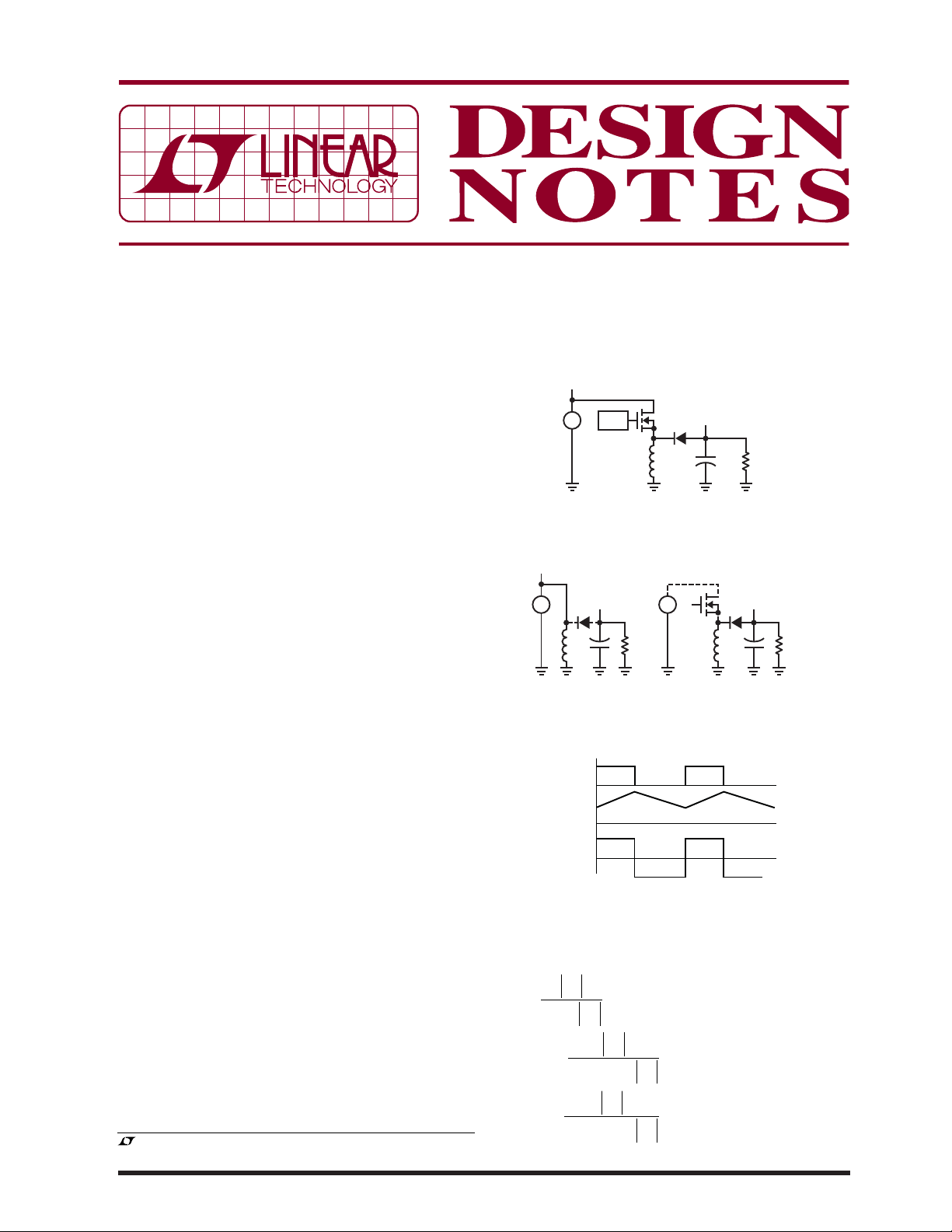
Basic Operation
Figure 1 shows a simplifi ed block diagram of a positive -tonegative converter. Figure 2 shows an equivalent circuit,
which helps in understanding the basic operation of the
circuit in Figure 1. When transistor Q is on (Figure 2a),
diode D is reverse biased and the current in inductor L
increases. When Q is off (Figure 2b), inductor L changes
polarity, diode D becomes forward biased, and current
fl ows from inductor L to the load and capacitor C. The
voltage across c apacitor C and the load is negative, rel ative
to system ground. Figure 3 shows a timing diagram.
, LTC and LT are registered trademarks of Linear Technology Corporation.
All other trademarks are the property of their respective owners.
The duty cycle range can be found from following
expression:
D
D
D
IN
–
+
V1
PWM
–
V
D
O
+
CR
LOAD
DN433 F01
Q
L
Figure 1. Simplifed Block Diagram of
Positive-to-Negative Converter
+
V
IN
–
+
–
(2a) Transistor Q is On (2b) Transistor Q is Off
V
O
V1
D
+
C
L
+
+
V1
–
R
LOAD
+
–
V
O
Q
D
C
L
R
LOAD
+
DN433 F02
Figure 2. Equivalent Circuits Show the Operation
of the Positive-to-Negative Converter
Q GATE
I
L
V
L
ON ONOFF
V
IN
V
OUT
OFF
DN433 F03
Figure 3. Converter Timing Diagram
V
O
=
VV
+
IN O
V
MAX
MIN
=
=
V
O
VV
IN MIN O
IN MAX
+
()
V
O
++ V
()
O
01/08/433
Component Stress in a Positive-to-Negative
Topology
V
is the maximum voltage across transistor Q and
MAX
diode D (Figure 2), where:
V
The max imum current, I
MAX
= V
IN(MAX)
+ |VO|
MAX
, through transistor Q, inductor L and diode D can be derived based on the following
equations, assuming continuous conduction mode:
I
I
L
O
== =+
1–
D
MAX
VtD
,
dI
••
IN MIN MAX
()
L
,
II
MAX L
II
d
2
where t is a switching period.
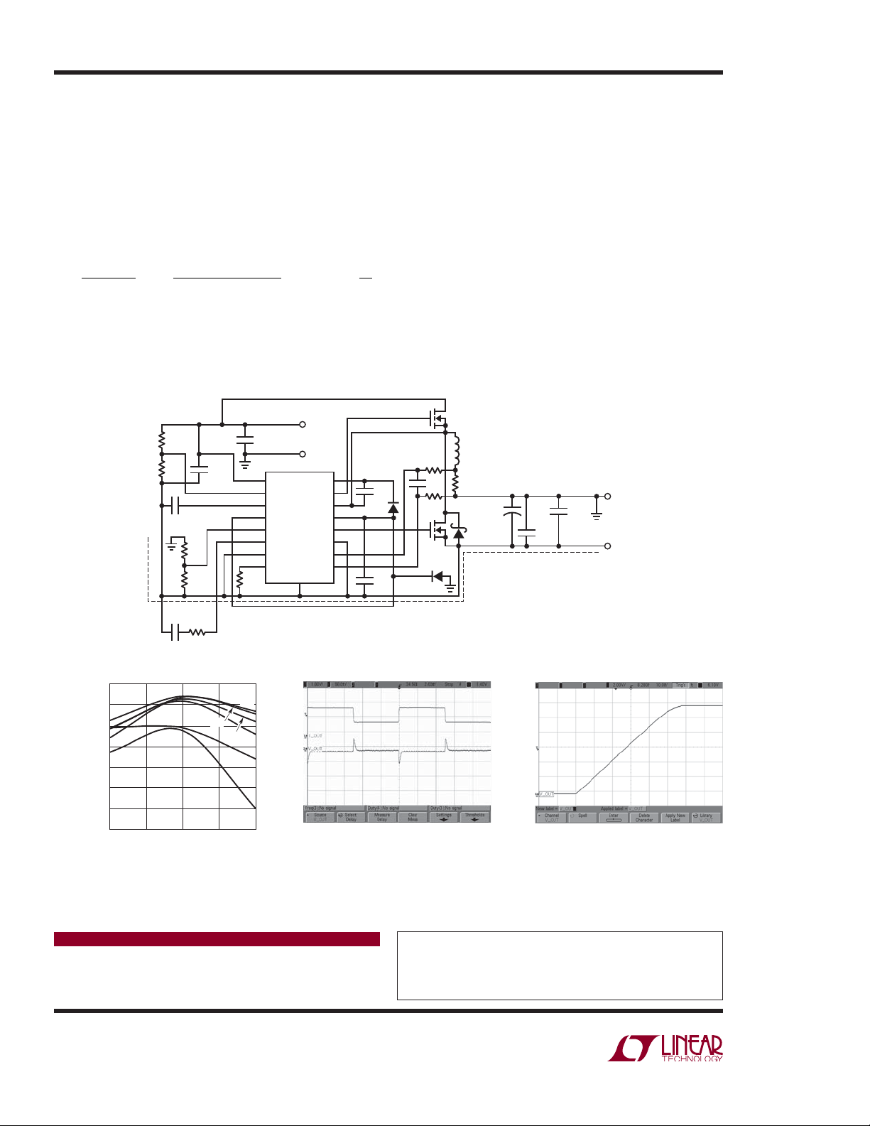
Circuit Description
Figure 4 shows a 9V to 15V input to –12V at 3A output
converter. The high voltage LT3845 is used for several
V
IN
R1
249k
R2
51.1k
C1
0.1μF
R3
143k
R4
16.2k
–12V (IC GND)
C4
2.2μF
61.9k
9V TO 15V
C
IN1
22μF
25V
C5
0.47μF
R5
R6
49.9k
1
2
3
4
5
6
7
8
V
IN
SHDN
SS
BURST
FB
V
C
SYNC
f
SET
LT3845
SGND
V
GND
17
IN
BOOST
PGND
16
C3
15
TG
SW
V
CC
BG
+
I
S
–
I
S
0.1μF
14
D2
BAS521
13
12
11
10
9
C2
1μF
reasons, including the ability of its SW pin to withstand
65V, its integrated high side driver and differential current sense. The LT3845 can also provide synchronous
rectifi cation, which allows the use of effi cient MOSFETs
over less effi cient switching diodes.
The entire conver ter power path contains t he LT3 845 high
voltage PWM controller, MOSFETs Q1 and Q2, inductor
L1, diode D1 and output fi lter capacitors C
OUT1–COUT3
Diode D2 is a bootstrap diode and diode D3 provides bias
voltage for internal MOSFET drivers.
Conclusion
Very often electrical engineers have to design a negative
voltage source supplied from a positive voltage rail. The
positive-to -negative converter discus sed in the article can
be a good alternative to a fl yback or a SEPIC approach.
Q1
PH3075L
L1
13μH
R8
PB2020.153
10Ω
C6
R
S1
OPT
R7
10Ω
PH1875L
D3 BAS521
–12V (IC GND)
Q2
6mΩ
C
OUT1
16ME470WF
D1
B160
DN433 F04
+
C
10μF
25V
OUT3
C
10μF
25V
OUT2
GND
V
–12V
3A
OUT
.
Figure 4. Conversion of 9V-15V into –12V at 3A Based on the LT3845 High Voltage PWM Controller
91.5
15V
14V
13V
12V
10V9V
2.5
DN433 F05
91.0
90.5
90.0
89.5
EFFICIENCY (%)
89.0
88.5
88.0
1.0
1.5 2.0 3.0
LOAD CURRENT (A)
Figure 5. Effi ciency for the Figure 4
Circuit with Varying Input Voltage to
a Fixed –12V Output
Data Sheet Download
www.linear.com
Linear Technology Corporation
1630 McCarthy Blvd., Milpitas, CA 95035-7417
(408) 432-1900
●
FAX: (408) 434-0507 ● www.linear.com
Figure 6. Transient Response to
an Output Load Step of 1A to 2A
call (408) 432-1900, Ext. 3161
Figure 7. Start-Up Waveform
for the Circuit in Figure 4 with
VIN = 14V, V
= –12V, I
OUT
For applications help,
dn433f LT/TP 0108 387K • PRINTED IN THE USA
© LINEAR TECHNOLOGY CORPORATION 2008
OUT
= 2A
 Loading...