

LT3825
Isolated No-Opto
Synchronous Flyback Controller
FEATURES
■
Senses Output Voltage Directly from Primary Side
Winding—No Optoisolator Required
■
Synchronous Driver for High Efficiency
■
Input Voltage Limited Only by External
Power Components
■
Accurate Output Regulation Without User Trims
■
Switching Frequency from 50kHz to 250kHz
■
Synchronizable
■
Load Compensation
■
Programmable Undervoltage Lockout
■
Available in a Thermally Enhanced 16-Lead
TSSOP Package
U
APPLICATIO S
■
Isolated Medium Power (10W to 60W) Supplies
■
Isolated Telecom, Medical Converters
■
Instrumentation Power Supplies
■
Isolated Power over Ethernet Supplies
with Wide Input Supply Range
U
DESCRIPTIO
The LT®3825 is an isolated switching regulator controller
designed for medium power flyback topologies. A typical
application is 10W to 60W with input voltage limited only
by external power path components. A third transformer
winding provides output voltage feedback.
The LT3825 is a current mode controller that regulates
output voltage based on sensing secondary voltage via a
transformer winding during flyback. This allows for tight
output regulation without the use of an optoisolator,
improving dynamic response and reliability. Synchronous
rectification increases converter efficiency and improves
output cross regulation in multiple output converters.
The LT3825 operates in forced continuous conduction
mode which improves cross regulation in multiple winding
applications. Switching frequency is user programmable
and can be externally synchronized. The part also has load
compensation, undervoltage lockout and soft-start circuity.
, LTC and LT are registered trademarks of Linear Technology Corporation.
All other trademarks are the property of their respective owners.
Protected by U.S. Patents, including 6948466, 5841643.
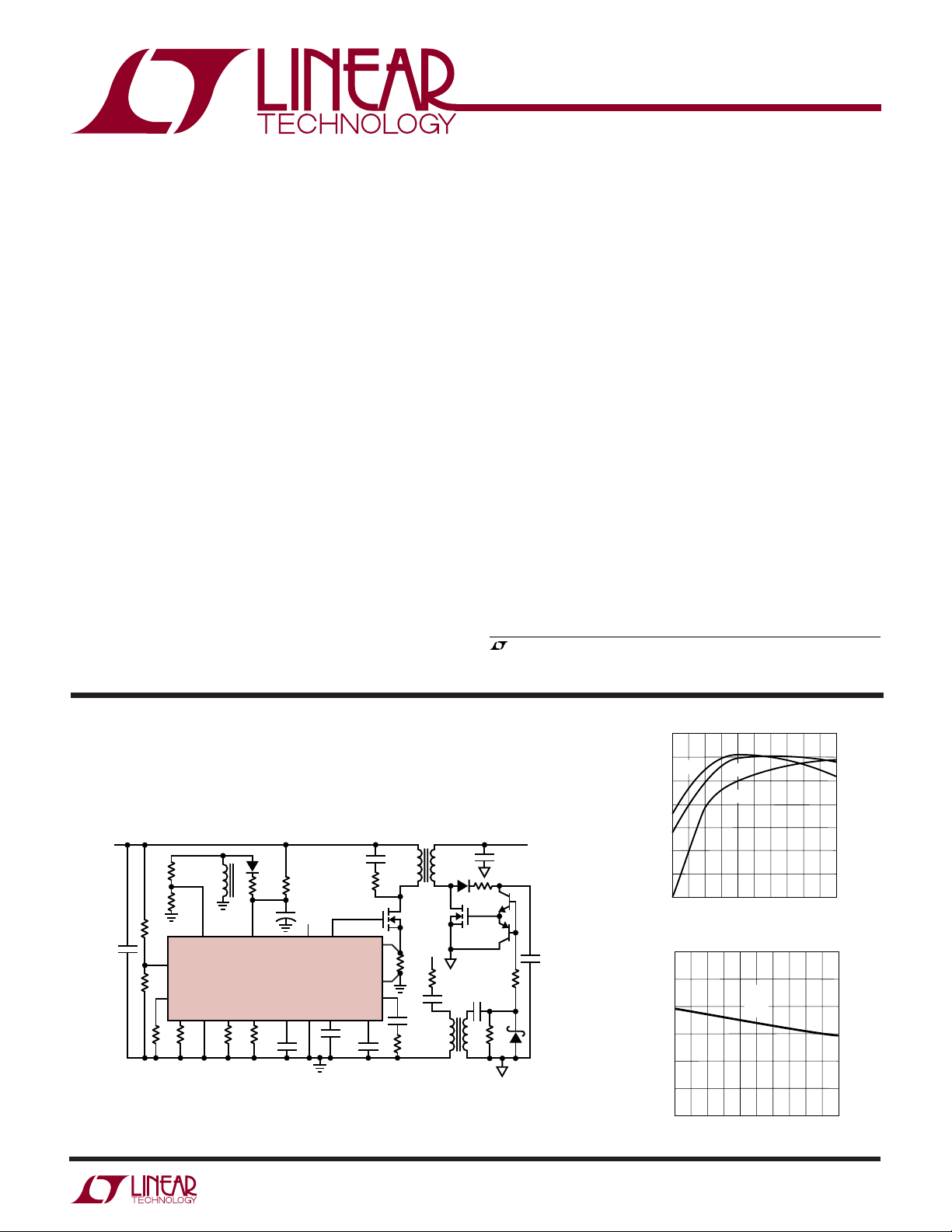
TYPICAL APPLICATIO
48V to 3.3V at 12A Isolated Supply
+
V
IN
36V TO 72V
28.7k
T1
20Ω
•
2.2µF
402k
15k
3.01k
UVLO
PGDLY
tONSYNC
100k12k
FB
R
CMP
47µF
V
CC
LT3825
ENDLY OSC
2.1k 150k
47pF
+
47k
SGSGPG
GND SFST
U
0.22µF
0.1µF
SENSE
SENSE
C
CMP
92
Efficiency
90
36V
IN
48V
88
86
+
V
OUT
3.3V
•
100pF
20Ω
+
–
V
C
0.02Ω
100k
10nF
T1
•
SG
330Ω
0.1µF
•
470µF
12A
×4
47Ω
×2
1µF
15Ω
2.2nF
•
10k
3825 TA01a
84
EFFICIENCY (%)
82
80
78
2
3
3.43
3.38
3.33
3.28
OUTPUT (V)
3.23
3.18
3.13
2
3
IN
72V
IN
5
6
4
LOAD CURRENT (A)
Regulation
5
6
4
LOAD CURRENT (A)
810
7
36V
IN
48V
IN
72V
IN
7
810
12
9
11
3825 TA01b
12
9
11
3825 TA01c
3825f
1
LT3825
WWWU
ABSOLUTE AXI U RATI GS
(Note 1)
VCC to GND
Low Impedance Source ........................ –0.3V to 18V
Current Fed
(VCC has Internal 19.5V Clamp) .......... 30mA into V
UVLO, SYNC Pin Voltage .......................... – 0.3V to V
SENSE–, SENSE+ Pin Voltage ................... – 0.5V, +0.5V
FB Pin Current ...................................................... ±2mA
V
Pin Current ..................................................... ±1mA
C
Operating Junction Temperature Range
(Notes 2, 3) .......................................... – 40°C to 125°C
Storage Temperature Range ................ –65°C to 150°C
Lead Temperature (Soldering, 10 sec).................. 300°C
CC
CC
UU
W
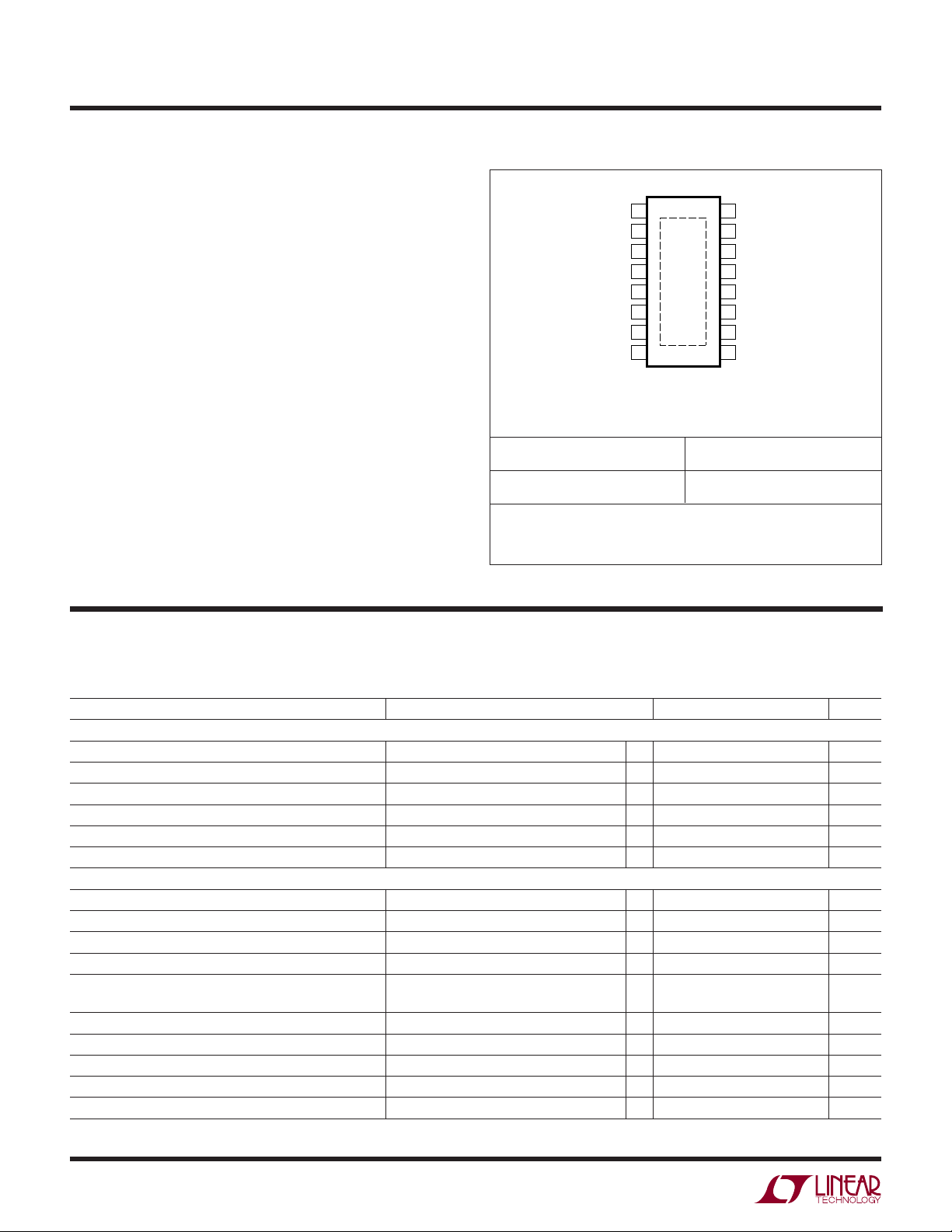
PACKAGE/ORDER I FOR ATIO
TOP VIEW
1
SG
2
V
CC
3
t
ON
4
ENDLY
SYNC
SFST
OSC
FB
16-LEAD PLASTIC TSSOP
T
= 125°C, θJA = 40°C/ W, θJC = 10°C/ W
JMAX
EXPOSED PAD (PIN 17) IS GND,MUST BE SOLDERED TO PCB
5
6
7
8
FE PACKAGE
17
ORDER PART NUMBER FE PART MARKING
LT3825EFE
Order Options Tape and Reel: Add #TR
Lead Free: Add #PBF Lead Free Tape and Reel: Add #TRPBF
Lead Free Part Marking: http://www.linear.com/leadfree/
Consult LTC Marketing for parts specified with wider operating temperature ranges.
PG
16
PGDLY
15
R
14
C
13
SENSE
12
SENSE
11
UVLO
10
V
9
CMP
CMP
+
–
C
3825EFE
ELECTRICAL CHARACTERISTICS
The ● denotes specifications which apply over the full operating temperature range, otherwise specifications are TA = 25°C.
= 14V; PG, SG Open; VC = 1.5V, V
V
CC
PARAMETER CONDITIONS MIN TYP MAX UNITS
Power Supply
VCC Turn-On Voltage
VCC Turn-Off Voltage
VCC Hysteresis V
VCC Shunt Clamp V
VCC Supply Current (Note 5) (ICC)V
VCC Start-Up Current VCC = 10V
Feedback Amplifier
Feedback Regulation Voltage (VFB)
Feedback Pin Input Bias Current R
Feedback Amplifier Transconductance ∆IC = ±10µA
Feedback Amplifier Source or Sink Current
Feedback Amplifier Clamp Voltage VFB = 0.9V 2.56 V
Reference Voltage Line Regulation 12V ≤ VCC ≤ 18V
Feedback Amplifier Voltage Gain VC = 1.2V to 1.7V 1400 V/V
Soft-Start Charging Current V
Soft-Start Discharge Current V
Control Pin Threshold (VC) Duty Cycle = Min 1.0 V
SENSE
–
= 0V; R
= 1k, R
CMP
CC(ON)
UVLO
= Open
C
Open 200 nA
CMP
= 1.4V 0.84 V
V
FB
= 0V 16 20 25 µA
SFST
= 1.5V, V
SFST
tON
– V
= 0V, I
= 90k, R
CC(OFF)
= 15mA
VCC
= 0V 0.8 1.3 mA
UVLO
PGDLY
= 27.4k, R
= 90k, unless otherwise specified.
ENDLY
●
14.0 15.3 16.0 V
●
●
●
●
●
●
●
●
●
8 9.7 11 V
4.0 5.6 6.5 V
19.5 20.5 V
4 6.4 10 mA
180 400 µA
1.220 1.237 1.251 V
700 1000 1400 µmho
25 55 90 µA
0.005 0.02 %/V
2
3825f
LT3825
ELECTRICAL CHARACTERISTICS
The ● denotes specifications which apply over the full operating temperature range, otherwise specifications are TA = 25°C.
= 14V; PG, SG Open; VC = 1.5V, V
V
CC
PARAMETER CONDITIONS MIN TYP MAX UNITS
Gate Outputs
PG, SG Output High Level
PG, SG Output Low Level
PG, SG Output Shutdown Strength V
PG Rise Time CPG = 1nF 11 ns
SG Rise Time CSG = 1nF 15 ns
PG, SG Fall Time CPG, CSG = 1nF 10 ns
Current Amplifier
Switch Current Limit at Maximum V
∆V
/∆V
SENSE
C
Sense Voltage Overcurrent Fault Voltage V
Timing
Switching Frequency (f
)C
OSC
Oscillator Capacitor Value (C
Minimum Switch On Time (t
Flyback Enable Delay Time (tED) 265 ns
PG Turn-On Delay Time (t
PGDLY
Maximum Switch Duty Cycle
SYNC Pin Threshold
SYNC Pin Input Resistance 40 kΩ
Load Compensation
Load Comp to V
Offset Voltage V
SENSE
Feedback Pin Load Compensation Current V
UVLO Function
UVLO Pin Threshold (V
UVLO
UVLO Pin Bias Current V
Note 1: Absolute Maximum ratings are those values beyond which the life
of a device may be impaired.
Note 2: This IC includes overtemperature protection that is intended to
protect the device during momentary overload conditions. Junction
temperature will exceed 125°C when overtemperature protection is active.
Continuous operation above the specified maximum operating junction
temperature may impair device reliability.
Note 3: The LT3825E is guaranteed to meet performance specifications
from 0°C to 125°C. Specifications over the –40°C to 125°C operating
temperature range are assured by design, characterization and correlation
with statistical process controls.
C
) (Note 6) 33 200 pF
OSC
) 200 ns
ON(MIN)
) 200 ns
)
SENSE
–
= 0V; R
CMP
V
= 1k, R
UVLO
SENSE
= 90k, R
tON
PGDLY
= 0V; IPG, ISG = 20mA
+
= 27.4k, R
= 90k, unless otherwise specified.
ENDLY
●
6.6 7.4 8.0 V
●
●
●
88 98 110 mV
0.01 0.05 V
1.4 1.8 V
0.07 V/V
+
, V
SENSE
OSC
RCMP
SENSE
UVLO
V
UVLO
= 100pF
< 1V
SFST
with V
+
= 20mV, VFB = 1.230V 20 µA
+
= 0V 1 mV
SENSE
= 1.2V –0.25 0 ±0.25 µA
= 1.3V –4.50 –3.4 –2.50 µA
Note 4: T
dissipation P
is calculated from the ambient temperature TA and power
J
according to the following formula:
D
= TA + (PD • 40°C/W)
T
J
●
●
84 100 110 kHz
●
85 88 %
●
●
1.215 1.240 1.265 V
206 230 mV
1.53 2.1 V
Note 5: Supply current does not include gate charge current to the
MOSFETs. See Applications Information.
Note 6: Component value range guaranteed by design.
3825f
3
LT3825
TEMPERATURE (°C)
–50
8
9
25 75
3825 G03
7
6
–25 0
50 100 125
5
4
3
10
I
VCC
(mA)
DYNAMIC CURRENT CPG = 1nF,
C
SG
= 1nF, f
OSC
= 100kHz
STATIC PART CURRENT
VCC = 14V
TEMPERATURE (°C)
–50
90
f
OSC
(kHz)
92
96
98
100
110
104
0
50
75
3825 G06
94
106
108
102
–25
25
100
125
C
OSC
= 100pF
TEMPERATURE (°C)
–50
V
FB
RESET (V)
1.03
25
3825 G09
1.00
0.98
–25 0 50
0.97
0.96
1.04
1.02
1.01
0.99
75 100 125
UW
TYPICAL PERFOR A CE CHARACTERISTICS
V
CC(ON)
vs Temperature
16
15
14
13
(V)
12
CC
V
11
10
9
8
–25 0 50
–50
and V
CC(OFF)
V
CC(ON)
V
CC(OFF)
25
TEMPERATURE (°C)
75 100 125
3825 G01
(µA)
VCC
I
Start-Up Current
V
CC
vs Temperature
300
250
200
150
100
50
0
–50
–25 0
50 100 125
25 75
TEMPERATURE (°C)
3825 G02
V
Current vs Temperature
CC
110
108
106
104
102
100
98
96
SENSE VOLTAGE (mV)
94
92
90
–50
1.240
1.239
1.238
1.237
1.236
(V)
1.235
FB
V
1.234
1.233
1.232
1.231
1.230
4
SENSE Voltage vs Temperature
FB = 1.1V
SENSE = V
WITH V
–25
vs Temperature
V
FB
–50
–25
+
SENSE
–
= 0V
SENSE
50
25
0
TEMPERATURE (°C)
50
25
0
TEMPERATURE (°C)
75
100
3825 G04
75
100
125
3825 G07
125
SENSE Fault Voltage
vs Temperature
220
SENSE = V
WITH V
215
210
205
200
195
SENSE VOLTAGE (mV)
190
185
180
–25 0 50
–50
+
SENSE
–
= 0V
SENSE
25
TEMPERATURE (°C)
Feedback Pin Input Bias
vs Temperature
300
R
OPEN
CMP
250
200
150
100
FEEDBACK PIN INPUT BIAS (nA)
50
0
–50
–25 0
25 75
TEMPERATURE (°C)
Oscillator Frequency
vs Temperature
75 100 125
3825 G05
VFB Reset vs Temperature
50 100 125
3825 G08
3825f
UW
TEMPERATURE (°C)
–50
3.4
3.5
3.7
25 75
3825 G15
3.3
3.2
–25 0
50 100 125
3.1
3.0
3.6
I
UVLO
(µA)
TEMPERATURE (°C)
–50 –25
19.0
V
CC
(V)
20.0
21.5
0
50
75
3825 G18
19.5
21.0
20.5
25
100
125
ICC = 10mA
TYPICAL PERFOR A CE CHARACTERISTICS
LT3825
Feedback Amplifier Output
Current vs V
70
50
30
10
(µA)
VC
I
–10
–30
–50
–70
0.9
FB
125°C
1
1.1
1.2
VFB (V)
1.3
Feedback Amplifier Voltage Gain
vs Temperature
1700
1650
1600
1550
1500
1450
1400
(V/V)
V
A
1350
1300
1250
1200
1150
1100
–25 0 50
–50
25
TEMPERATURE (°C)
25°C
–40°C
1.5
1.4
3825 G10
75 100 125
3825 G13
Feedback Amplifier Source and
Sink Current vs Temperature
70
65
60
(µA)
55
VC
I
50
45
40
–50
–25 0
SOURCE CURRENT
25 75
TEMPERATURE (°C)
= 1.1V
V
FB
50 100 125
SINK
CURRENT
= 1.4V
V
FB
3825 G11
UVLO vs Temperature I
1.250
1.245
1.240
1.235
UVLO (V)
1.230
1.225
1.220
–50
–25 0
TEMPERATURE (°C)
50 100 125
25 75
3825 G14
Feedback Amplifier g
vs Temperature
1100
1050
1000
(µmho)
m
g
950
900
–50
–25 0 25 50
TEMPERATURE (°C)
Hysteresis vs Temperature
UVLO
m
75 100 125
3825 G12
Soft-Start Charge Current
vs Temperature
23
22
21
20
19
18
17
SFST CHARGE CURRENT (µA)
16
15
–25 0 50
–50
TEMPERATURE (°C)
PG, SG Rise and Fall Times
vs Load Capacitance
80
TA = 25°C
70
60
50
40
TIME (ns)
30
20
10
0
0
75 100 125
3825 G16
25
FALL TIME
RISE TIME
246 107135 9
CAPACITANCE (nF)
8
3825 G17
VCC Clamp Voltage
vs Temperature
3825f
5
LT3825
UW
TYPICAL PERFOR A CE CHARACTERISTICS
Minimum PG On Time
vs Temperature
340
R
tON(MIN)
330
320
310
(ns)
300
ON(MIN)
t
290
280
270
260
–25 0 50
–50
U
= 158k
25
TEMPERATURE (°C)
75 100 125
3825 G19
UU
PG Delay Time vs Temperature
300
250
200
(ns)
150
PGDLY
t
100
50
0
–50
–25 25
R
R
0
TEMPERATURE (°C)
PI FU CTIO S
SG (Pin 1): Synchronous Gate Drive Output. This pin
provides an output signal for a secondary-side synchronous switch. Large dynamic currents may flow during
voltage transitions. See the Applications Information for
details.
V
(Pin 2): Supply Voltage Pin. Bypass this pin to ground
CC
with a 4.7µF capacitor or more. This pin has a 19.5V clamp
to ground. V
turns the part on when V
at 9.7V. In a conventional “trickle-charge” bootstrapped
configuration, the V
cantly during turn-on causing a benign relaxation oscillation action on the VCC pin if the part does not start
normally.
(Pin 3): Pin for external programming resistor to set
t
ON
the minimum time that the primary switch is on for each
cycle. Minimum turn-on facilitates the isolated feedback
method. See Applications Information for details.
has an undervoltage lockout function that
CC
is approximately 15.3V and off
CC
supply current increases signifi-
CC
Enable Delay Time vs Temperature
260
R
= 90k
ENDLY
PGDLY
PGDLY
= 27.4k
= 16.9k
50
75
100 125
3825 G20
240
(ns)
ED
t
180
140
220
200
160
–50
–25 0
50 100 125
25 75
TEMPERATURE (°C)
SYNC (Pin 5): Pin for synchronizing the internal oscillator
with an external clock. The positive edge on a pulse causes
the oscillator to discharge causing PG to go low (off) and
SG high (on). The sync threshold is typically 1.6V. See
Applications Information for details. Tie to ground if
unused.
SFST (Pin 6): This pin, in conjunction with a capacitor to
ground, controls the ramp-up of peak primary current as
sensed through the sense resistor. This is used to control
converter inrush current at start-up. The VC pin voltage
cannot exceed the SFST pin voltage, so as SFST increases,
the maximum voltage on VC increases commensurately,
allowing higher peak currents. Total V
ramp time is
C
approximately 70ms per µF of capacitance. Leave pin open
if not using the soft-start function.
OSC (Pin 7): This pin in conjunction with an external
capacitor defines the controller oscillator frequency. The
frequency is approximately 100kHz • 100/C
OSC
(pF).
3825 G21
ENDLY (Pin 4): Pin for external programming resistor to
set enable delay time. The enable delay time disables the
feedback amplifier for a fixed time after the turn-off of the
primary-side MOSFET. This allows the leakage inductance
voltage spike to be ignored for flyback voltage sensing.
See Applications Information for details.
6
FB (Pin 8): Pin for the feedback node for the power supply
feedback amplifier. Feedback is usually sensed via a third
winding and enabled during the flyback period. This pin
also sinks additional current to compensate for load
current variation as set by the R
pin. Keep the Thevenin
CMP
equivalent resistance of the feedback divider at roughly 3k.
3825f

LT3825
U
UU
PI FU CTIO S
VC (Pin 9): Pin used for frequency compensation for the
switcher control loop. It is the output of the feedback
amplifier and the input to the current comparator. Switcher
frequency compensation components are normally placed
on this pin to ground. The voltage on this pin is proportional to the peak primary switch current. The feedback
amplifier output is enabled during the synchronous switch
on time.
UVLO (Pin 10): A resistive divider from V
an undervoltage lockout based upon V
When the UVLO pin is below its threshold, the gate drives
are disabled, but the part draws its normal quiescent
current from VCC. The VCC undervoltage lockout supersedes this function so V
the part.
The bias current on this pin has hysteresis such that the
bias current is sourced when the UVLO threshold is
exceeded. This introduces a hysteresis at the pin equivalent to the bias current change times the impedance of the
upper divider resistor. The user can control the amount of
hysteresis by adjusting the impedance of the divider. See
the Applications Information for details. Tie the UVLO pin
to V
SENSE– (Pin 11), SENSE+ (Pin 12): These pins are used
to measure primary side switch current through an external sense resistor. Peak primary side current is used in the
converter control loop. Make Kelvin connections to the
if you are not using this function.
CC
must be great enough to start
CC
to this pin sets
IN
level (not VCC).
IN
sense resistor to reduce noise problems. SENSE– connects to the ground side. At maximum current (V
maximum voltage) it has a 98mV threshold. The signal is
blanked (ignored) during the minimum turn-on time.
C
(Pin 13): Pin for external filter capacitor for the op-
CMP
tional load compensation function. Load compensation
reduces the effects of parasitic resistances in the feedback
sensing path. A 0.1µF ceramic capacitor suffices for most
applications. Short this pin to GND in less demanding
applications that don’t require load compensation.
R
(Pin 14): Pin for optional external load compensa-
CMP
tion resistor. Use of this pin allows for nominal compensation of parasitic resistances in the feedback sensing
path. In less demanding applications, this resistor is not
needed and this pin can be left open. See Applications
Information for details.
PGDLY (Pin 15): Pin for external programming resistor to
set delay from synchronous gate turn-off to primary gate
turn-on. See Applications Information for details.
PG (Pin 16): Gate Drive Pin for the Primary Side MOSFET
Switch. Large dynamic currents flow during voltage transitions. See the Applications Information for details.
GND (Exposed Pad, Pin 17): This is the ground connection for both signal ground and gate driver grounds. This
GND should be connected to the PCB ground plane.
Careful attention must be paid to ground layout. See
Applications Information for details.
at its
C
3825f
7
LT3825
BLOCK DIAGRA
W
2
10
V
15.3V
UVLO
CC
V
UVLO
CC
+
–
REFERENCE
1.235V
(V
FB
19.5V
+
–
)
INTERNAL
REGULATOR
+
UVLO
–
I
UVLO
TSD
CURRENT TRIP
CLAMPS
0.7
1.3
3V
–
+
SRQ
CURRENT
COMPARATOR
ERROR AMP
Q
COLLAPSE DETECT
–
+
1V
OVERCURRENT
–
FAULT
–
–
+
CURRENT
SENSE AMP
+
+
SFST
SENSE
FB
8
V
C
9
6
–
11
+
SLOPE COMPENSATION
OSC
7
SYNC
5
t
ON
3
PGDLY
15
ENDLY
4
OSCILLATOR
SET
ENABLE
LOGIC
BLOCK
TO FB
PGATE
SGATE
R
CMPF
50k
+
GATE DRIVE
–
V
CC
SENSE
C
CMP
LOAD
COMPENSATION
R
CMP
PG
12
13
14
16
+
3V
–
V
CC
GATE DRIVE
SG
GND
1
17
8
3825f
W
FLYBACK FEEDBACK A PLIFIER
LT3825
R1
FB
8
R2
–
UWW
TI I G DIAGRA
LT3825 FEEDBACK AMP
1V
V
FB
1.25V
+
COLLAPSE
DETECT
ENABLE
–
+
SRQ
V
FLBK
V
T1
FLYBACK
•
C
9
3825 FFA
V
IN
C
VC
V
PRIMARY
MP
IN
•
SECONDARY
•
MS
ISOLATED
C
OUT
OUTPUT
PRIMARY SIDE
MOSFET DRAIN
VOLTAGE
PG VOLTAGE
SG VOLTAGE
V
IN
t
ON(MIN)
ENABLE
DELAY
V
FLBK
MIN ENABLE
FEEDBACK
AMPLIFIER
ENABLED
0.8 • V
FLBK
PG DELAY
3825 TD
3825f
9

LT3825
OPERATIO
U
The LT3825 is a current mode switcher controller IC
designed specifically for use in an isolated flyback topology employing synchronous rectification. The LT3825
operation is similar to traditional current mode switchers.
The major difference is that output voltage feedback is
derived via sensing the output voltage through the transformer. This precludes the need of an optoisolator in
isolated designs greatly improving dynamic response and
reliability. The LT3825 has a unique feedback amplifier
that samples a transformer winding voltage during the
flyback period and uses that voltage to control output
voltage.
The internal blocks are similar to many current mode
controllers. The differences lie in the flyback feedback
amplifier and load compensation circuitry. The logic block
also contains circuitry to control the special dynamic
requirements of flyback control.
For more information on the basics of current mode
switcher/controllers and isolated flyback converters see
Application Note 19.
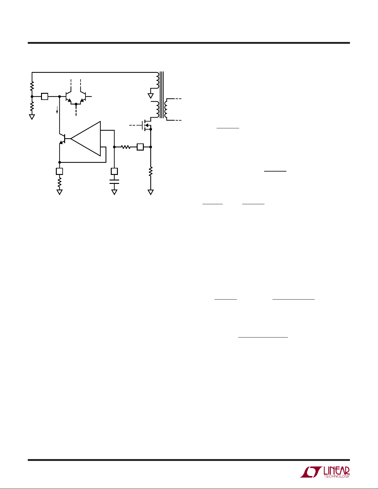
Feedback Amplifier—Pseudo DC Theory
For the following discussion refer to the simplified Flyback
Feedback Amplifier diagram. When the primary side MOSFET switch MP turns off, its drain voltage rises above the
V
rail. Flyback occurs when the primary MOSFET is off
IN
and the synchronous secondary MOSFET is on. During
flyback the voltage on nondriven transformer pins is
determined by the secondary voltage. The amplitude of
this flyback pulse as seen on the third winding is given as:
VI ESRR
++
•
V
FLBK
R
DS(ON)
I
= transformer secondary current
SEC
ESR = impedance of secondary circuit capacitor, winding
and traces
= transformer effective secondary-to-feedback wind-
N
SF
ing turns ratio (i.e., N
The flyback voltage is scaled by an external resistive
divider R1/R2 and presented at the FB pin. The feedback
OUT SEC DS ON
=
= on resistance of the synchronous MOSFET M
()
N
SF
S/NFLBK
)
()
S
amplifier compares the voltage to the internal bandgap
reference. The feedback amp is actually a transconductance
amplifier whose output is connected to V
period in the flyback time. An external capacitor on the V
pin integrates the net feedback amp current to provide the
control voltage to set the current mode trip point.
The regulation voltage at the FB pin is nearly equal to the
bandgap reference VFB because of the high gain in the
overall loop. The relationship between V
expressed as:
RR
V
FLBK FB
Combining this with the previous V
an expression for V
programming resistors and secondary resistances:
V
=
OUT FB SF SEC DS ON
The effect of nonzero secondary output impedance is
discussed in further detail; see Load Compensation Theory.
The practical aspects of applying this equation for V
found in the Applications Information.
Feedback Amplifier Dynamic Theory
So far, this has been a pseudo-DC treatment of flyback
feedback amplifier operation. But the flyback signal is a
pulse, not a DC level. Provision must be made to enable the
flyback amplifier only when the flyback pulse is present.
This is accomplished by the “Enable” line in the diagram.
Timing signals are then required to enable and disable the
flyback amplifier. There are several timing signals which
are required for proper LT3825 operation. Please refer to
the Timing Diagram.
Minimum Output Switch On Time (t
The LT3825 affects output voltage regulation via flyback
pulse action. If the output switch is not turned on, there
is no flyback pulse and output voltage information is not
available. This causes irregular loop response and startup/latch-up problems. The solution is to require the
primary switch to be on for an absolute minimum time per
each oscillator cycle. If the output load is less than that
=
R
RR
+
12
⎛
⎜
⎝
R
2
+12
V
•
2
FLBK
in terms of the internal reference,
OUT
VN I ESRR
•• – •
⎞
⎟
⎠
only during a
C
C
and VFB is
FLBK
expression yields
+
(()
ON(MIN)
)
()
OUT
are
3825f
10

R
ESR R
DC
S OUT
DS ON
()
()
–
=
+
1
OPERATIO
LT3825
U
developed under these conditions, forced continuous
operation normally occurs. See Applications Information
for further details.
Enable Delay (ENDLY)
The flyback pulse appears when the primary side switch
shuts off. However, it takes a finite time until the transformer primary side voltage waveform represents the
output voltage. This is partly due to rise time on the
primary side MOSFET drain node but, more importantly, is
due to transformer leakage inductance. The latter causes
a voltage spike on the primary side, not directly related to
output voltage. Some time is also required for internal
settling of the feedback amplifier circuitry. In order to
maintain immunity to these phenomena, a fixed delay is
introduced between the switch turn-off command and the
enabling of the feedback amplifier. This is termed “enable
delay.” In certain cases where the leakage spike is not
sufficiently settled by the end of the enable delay period,
regulation error may result. See Applications Information
for further details.
enable time described to a maximum of roughly the “off”
switch time minus the enable delay time. Certain parameters of feedback amp behavior are directly affected by
the variable enable period. These include effective
transconductance and V
node slew rate.
C
Load Compensation Theory
The LT3825 uses the flyback pulse to obtain information
about the isolated output voltage. An error source is
caused by transformer secondary current flow through the
synchronous MOSFET R
and real life nonzero im-
DS(ON)
pedances of the transformer secondary and output capacitor. This was represented previously by the expression
“I
• (ESR + R
SEC
).” However, it is generally more
DS(ON)
useful to convert this expression to effective output impedance. Because the secondary current only flows during
the off portion of the duty cycle (DC), the effective output
impedance equals the lumped secondary impedance divided by OFF time DC.
Since the OFF time duty cycle is equal to 1 – DC then:
Collapse Detect
Once the feedback amplifier is enabled, some mechanism
is then required to disable it. This is accomplished by a
collapse detect comparator, which compares the flyback
voltage (FB referred) to a fixed reference, nominally 80%
of V
. When the flyback waveform drops below this level,
FB
the feedback amplifier is disabled.
Minimum Enable Time
The feedback amplifier, once enabled, stays enabled for a
fixed minimum time period termed “minimum enable
time.” This prevents lockup, especially when the output
voltage is abnormally low; e.g., during start-up. The minimum enable time period ensures that the V
node is able
C
to “pump up” and increase the current mode trip point to
the level where the collapse detect system exhibits proper
operation. This time is set internally.
Effects of Variable Enable Period
The feedback amplifier is enabled during only a portion of
the cycle time. This can vary from the fixed minimum
where:
R
= effective supply output impedance
S(OUT)
DC = duty cycle
R
and ESR are as defined previously
DS(ON)
This impedance error may be judged acceptable in less
critical applications, or if the output load current remains
relatively constant. In these cases the external FB resistive
divider is adjusted to compensate for nominal expected
error. In more demanding applications, output impedance
error is minimized by the use of the load compensation
function.
Figure 1 shows the Block Diagram of the load compensation function. Switch current is converted to a voltage by
the external sense resistor, averaged and lowpass filtered
by the internal 50k resistor R
capacitor on C
external R
CMP
. This voltage is impressed across the
CMP
resistor by op amp A1 and transistor Q3
and the external
CMPF
producing a current at the collector of Q3 that is
3825f
11
LT3825
OPERATIO
R1
FB
Q1 Q2
Q3
R
14 13
CMP
Figure 1. Load Compensation Diagram
R2
8
LOAD
COMP I
U
V
FLBK
T1
Average primary side current is expressed in terms of
output current as follows:
•
IKI
==11•
V
FB
+
R
C
CMPF
50k
CMP
A1
–
SENSE
12
V
IN
•
•
MP
+
R
SENSE
3825 F01
IN OUT
where
:
V
K
OUT
V Eff
•
IN
So the effective change in V
R
∆ = ∆
VKI
OUT OUT
thus
:
V
∆
OUT
∆
II
OUT
11•• ••
= 11•••
K
R
SENSE
R
CMP
SENSE
R
RN
target is:
OUT
CMP
RN
SF
SF
subtracted from the FB node. This effectively increases
the voltage required at the top of the R1/R2 feedback
divider to achieve equilibrium.
The average primary side switch current increases to
maintain output voltage regulation as output loading increases. The increase in average current increases the
R
resistor current which affects a corresponding in-
CMP
crease in sensed output voltage, compensating for the IR
drops.
Assuming a relatively fixed power supply efficiency, Eff,
power balance gives:
= Eff • P
P
V
OUT
OUT
• I
IN
= Eff • VIN • I
OUT
IN
where:
K1 = dimensionless variable related to V
IN
, V
OUT
and
efficiency as explained above
R
= external sense resistor
SENSE
Nominal output impedance cancellation is obtained by
equating this expression with R
R
SENSE
K
11
•••
R
CMP
Solving for R
RK
=
CMP
RN
gives:
CMP
RDC
SENSE
1
ESR R
ESR R
=
SF
11••–
()
+
()
DS ON
S(OUT)
+
1
–
DC
••
RN
:
()
DS ON
SF
The practical aspects of applying this equation to determine an appropriate value for the R
resistor are found
CMP
in the Applications Information.
12
3825f

WUUU
APPLICATIO S I FOR ATIO
LT3825
Transformer Design
Transformer design/specification is the most critical part
of a successful application of the LT3825. The following
sections provide basic information about designing the
transformer and potential tradeoffs.
If you need help, the LTC Applications group is available to
assist in the choice and/or design of the transformer.
Turns Ratios
The design of the transformer starts with determining duty
cycle (DC). DC impacts the current and voltage stress on
the power switches, input and output capacitor RMS
currents and transformer utilization (size vs power).
The ideal turns ratio is:
N
IDEAL
V
OUT
= •
V
IN
–1
DC
DC
Avoid extreme duty cycles as they, in general, increase
current stresses. A reasonable target for duty cycle is 50%
at nominal input voltage.
For instance, if we wanted a 48V to 5V converter at 50% DC
then:
548105051
N
IDEAL
==
–.
•
..
96
In general, better performance is obtained with a lower
turns ratio. A DC of 45.5% yields a 1:8 ratio.
Note the use of the external feedback resistive divider ratio
to set output voltage provides the user additional freedom
in selecting a suitable transformer turns ratio. Turns ratios
that are the simple ratios of small integers; e.g., 1:1, 2:1,
3:2 help facilitate transformer construction and improve
performance.
When building a supply with multiple outputs derived
through a multiple winding transformer, lower duty cycle
can improve cross regulation by keeping the synchronous
rectifier on longer, and thus, keep secondary windings
coupled longer.
For a multiple output transformer, the turns ratio between
output windings is critical and affects the accuracy of the
voltages. The ratio between two output voltages is set with
the formula V
OUT2
= V
• N21 where N21 is the turns
OUT1
ratio between the two windings. Also keep the secondary
MOSFET R
small to improve cross regulation.
DS(ON)
The feedback winding usually provides both the feedback
voltage and power for the LT3825. So set the turns ratio
between the output and feedback winding to provide a
rectified voltage that under worst-case conditions is greater
than the 11V maximum V
V
N
SF
For our example:
We will choose
OUT
>
+
V
11
F
N
SF
1
turn-off voltage.
CC
5
>
11 0 71.
=
+
2234.
3
Leakage Inductance
Transformer leakage inductance (on either the primary or
secondary) causes a spike after the primary side switch
turn-off. This is increasingly prominent at higher load
currents, where more stored energy is dissipated. Higher
flyback voltage may break down the MOSFET switch if it
has too low a BV
DSS
rating.
One solution to reducing this spike is to use a snubber
circuit to suppress the voltage excursion. However, suppressing the voltage extends the flyback pulse width. If the
flyback pulse extends beyond the enable delay time,
output voltage regulation is affected. The feedback system
has a deliberately limited input range, roughly ±50mV
referred to the FB node. This rejects higher voltage leakage
spikes because once a leakage spike is several volts in
amplitude, a further increase in amplitude has little effect
on the feedback system.
Therefore, it is advisable to arrange the snubber circuit to
clamp at as high a voltage as possible, observing MOSFET
breakdown, such that leakage spike duration is as short as
possible. Application Note 19 provides a good reference
on snubber design.
3825f
13

LT3825
WUUU
APPLICATIO S I FOR ATIO
As a rough guide, leakage inductance of several percent (of
mutual inductance) or less may require a snubber, but
exhibit little to no regulation error due to leakage spike
behavior. Inductances from several percent up to perhaps
ten percent cause increasing regulation error.
Avoid double digit percentage leakage inductances as there
is a potential for abrupt loss of control at high load current.
This curious condition potentially occurs when the leakage
spike becomes such a large portion of the flyback waveform
that the processing circuitry is fooled into thinking that the
leakage spike itself is the real flyback signal!
It then reverts to a potentially stable state whereby the top
of the leakage spike is the control point, and the trailing edge
of the leakage spike triggers the collapse detect circuitry.
This typically reduces the output voltage abruptly to a fraction, roughly one-third to two-thirds of its correct value.
Once load current is reduced sufficiently, the system
snaps back to normal operation. When using transformers with considerable leakage inductance, exercise this
worst-case check for potential bistability:
1. Operate the prototype supply at maximum expected
load current.
2. Temporarily short circuit the output.
3. Observe that normal operation is restored.
If the output voltage is found to hang up at an abnormally
low value, the system has a problem. This is usually
evident by simultaneously viewing the primary side
MOSFET drain voltage to observe firsthand the leakage
spike behavior.
A final note—the susceptibility of the system to bistable
behavior is somewhat a function of the load current/
voltage characteristics. A load with resistive—i.e., I = V/R
behavior—is the most apt to be bistable. Capacitive loads
that exhibit I = V
2
/R behavior are less susceptible.
Secondary Leakage Inductance
Leakage inductance on the secondary forms an inductive
divider on the transformer secondary, reducing the size of
the feedback flyback pulse. This increases the output
voltage target by a similar percentage.
Note that unlike leakage spike behavior, this phenomenon
is independent of load. Since the secondary leakage inductance is a constant percentage of mutual inductance
(within manufacturing variations), the solution is to adjust
the feedback resistive divider ratio to compensate.
Winding Resistance Effects
Primary or secondary winding resistance acts to reduce
overall efficiency (P
increases effective output impedance degrading load regulation. Load compensation can mitigate this to some extent but a good design keeps parasitic resistances low.
Bifilar Winding
A bifilar or similar winding is a good way to minimize
troublesome leakage inductances. Bifilar windings also
improve coupling coefficients and thus improve cross
regulation in multiple winding transformers. However,
tight coupling usually increases primary-to-secondary
capacitance and limits the primary-to-secondary breakdown voltage, so it isn’t always practical.
Primary Inductance
The transformer primary inductance, L
on the peak-to-peak ripple current ratio (X) in the transformer relative to its maximum value. As a general rule,
keep X in the range of 20% to 40% ripple current (i.e., X
= 0.2 to 0.4). Higher values of ripple will increase conduction losses, while lower values will require larger cores.
OUT/PIN
). Secondary winding resistance
, is selected based
P
14
3825f

WUUU
APPLICATIO S I FOR ATIO
LT3825
Ripple current and percentage ripple is largest at minimum duty cycle; in other words, at the highest input
voltage. L
L
=
P
is calculated from:
P
VDC
()
IN MAX MIN
fX P
OSC MAX IN
•
() ()
••
V
()
IN MAX
=
fX P
OSC MAX OUT
•2DDC Eff
••
MIN
2
•
where:
is the oscillator frequency
f
OSC
DC
is the DC at maximum input voltage
MIN
is ripple current ratio at maximum input voltage
X
MAX
For a 48V (V
efficiency, P
and f
OSC
DC
MIN
L
=
P
= 36V to 72V) to 5V/8A converter with 90%
IN
= 40W and PIN = 44.44W. Using X = 0.4
OUT
= 200kHz:
=
1
()
200 0 4 44 44
kHz W
1
•
NV
+
7
IN MAX
V
OUT
22 0 357
V
•.
•.• .
=
()
2
1
1872
•
+
1
5
=µ
186
H
=
35 7
.%
The main design goals for core selection are reducing
copper losses and preventing saturation. Ferrite core
material saturates hard, rapidly reducing inductance when
the peak design current is exceeded. This results in an
abrupt increase in inductor ripple current and, consequently, output voltage ripple. Do not allow the core to
saturate! The maximum peak primary current occurs at
minimum V
I
PK
now
DC
X
Using the example numbers leads to:
:
IN
P
=+
VDC
IN MIN MAX
XX
MA
=
MIN
=
IN
•
()
=
1
V
()
.
0 202
1
•
NV
()
IN MIN
+
V
OUT
DC
I
•
NNMIN MAX
()
fLP k
••
OSC P IN
⎛
•:1
⎜
⎝
=
X
⎞
MIN
⎟
⎠
2
1
=
52 6
1836
+
1
•
5
2
=
()
200
.%
36 52 6
•.%
HHz H••.
186 44 44
2
µ
Optimization might show that a more efficient solution is
obtained at higher peak current but lower inductance and
the associated winding series resistance. A simple spreadsheet program is useful for looking at tradeoffs.
Transformer Core Selection
Once L
is known, the type of transformer is selected. High
P
efficiency converters use ferrite cores to minimize core
loss. Actual core loss is independent of core size for a fixed
inductance, but decreases as inductance increases. Since
increased inductance is accomplished through more turns
of wire, copper losses increase. Thus transformer design
balances core and copper losses. Remember that increased winding resistance will degrade cross regulation
and increase the amount of load compensation required.
44 44
W
I
PK
.
=+
36 0 526
•.
0 202
.
⎛
1
•
⎜
⎝
⎞
=
⎟
⎠
2
258
.
A
Multiple Outputs
One advantage that the flyback topology offers is that
additional output voltages can be obtained simply by
adding windings. Designing a transformer for such a
situation is beyond the scope of this document. For
multiple windings, realize that the flyback winding signal
is a combination of activity on all the secondary windings.
Thus load regulation is affected by each windings load.
Take care to minimize cross regulation effects.
3825f
15
LT3825
RK
RDC
ESR R
RN R
CMP
SENSE
DS ON
SF
=
()
+
=1
11••–
••
()
SS OUT()
WUUU
APPLICATIO S I FOR ATIO
Setting Feedback Resistive Divider
The expression for V
developed in the Operation sec-
OUT
tion is rearranged to yield the following expression for the
feedback resistors:
⎛
12 1=
⎜⎜
⎜
⎝
RR
⎡
VI ESRR
OUT SEC DS ON
⎣
•
++
()
•
VN
FB SF
Continuing the example, if ESR + R
()
= 8mΩ, R2 =
DS(ON)
⎞
⎤
⎦
⎟
–
⎟
⎠
3.32k, then:
Rk k134
⎛
⎜
⎝
•.
1 232 1 3
.•/
⎞
1376=
=.
–.
⎟
⎠
5 8 0 008
+
choose 37.4k.
It is recommended that the Thevenin impedance of the
resistive divider (R1||R2) is roughly 3k for bias current
cancellation and other reasons.
Current Sense Resistor Considerations
above nominal so I
on R
and minimum V
SENSE
110% = 80mV/3.64A and nominal R
= 3.64A . If there is a 10% tolerance
PK
= 80mV, then R
SENSE
= 20mΩ. Round
SENSE
to the nearest available lower value.
Selecting the Load Compensation Resistor
The expression for R
was derived in the Operation
CMP
section as:
Continuing the example:
⎛
K
1
⎜
⎝
If ESR R
R
+
CMP
V
VEff
IN
DSS(ON)
=
⎞
OUT
⎟
••%
⎠
= Ω
0 116
.•
5
==
.
0 116=
48 90
m
8
m
20 1 0 455
•–.
Ω
()
m
8
37 4
•.ΩkkkΩ
= 196.
SENSE
•
The external current sense resistor is used to control peak
primary switch current, which controls a number of key
converter characteristics including maximum power and
external component ratings. Use a noninductive current
sense resistor (no wire-wound resistors). Mounting the
resistor directly above an unbroken ground plane connected with wide and short traces keeps stray resistance
and inductance low.
The dual sense pins allow for a fully Kelvined connection.
Make sure that SENSE
+
and SENSE– are isolated and
connect close to the sense resistor to preserve this.
Peak current occurs at 98mV of sense voltage V
the nominal sense resistor is V
SENSE/IPK.
For example, a
SENSE
. So
peak switch current of 10A requires a nominal sense resistor of 0.010Ω. Note that the instantaneous peak power in
the sense resistor is 1W, and that it is rated accordingly.
The use of parallel resistors can help achieve low resistance,
low parasitic inductance and increased power capability.
Size R
V
SENSE
using worst-case conditions, minimum LP,
SENSE
and maximum VIN. Continuing the example, let us
assume that our worst-case conditions yield an IPK 40%
This value for R
is a good starting point, but empirical
CMP
methods are required for producing the best results. This
is because several of the required input variables are
difficult to estimate precisely. For instance, the ESR term
above includes that of the transformer secondary, but its
effective ESR value depends on high frequency behavior,
not simply DC winding resistance. Similarly, K1 appears
as a simple ratio of V
to V
IN
times (differential) effi-
OUT
ciency, but theoretically estimating efficiency is not a
simple calculation.
The suggested empirical method is as follows:
1. Build a prototype of the desired supply including the
actual secondary components.
2. Temporarily ground the C
pin to disable the load
CMP
compensation function. Measure output voltage while
sweeping output current over the expected range.
Approximate the voltage variation as a straight line,
∆V
/∆I
OUT
= R
OUT
3. Calculate a value for the K1 constant based on VIN, V
S(OUT)
.
OUT
and the measured efficiency.
16
3825f

WUUU
APPLICATIO S I FOR ATIO
LT3825
4. Compute:
R
RK
= 11•••
CMP
SENSE
R
S OUT
()
RN
SF
5. Verify this result by connecting a resistor of this value
from the R
6. Disconnect the ground short to C
pin to ground.
CMP
and connect a
CMP
0.1µF filter capacitor to ground. Measure the output
impedance R
pensation in place. R
S(OUT)
= ∆V
S(OUT)
/∆I
OUT
with the new com-
OUT
should have decreased
significantly. Fine tuning is accomplished experimentally by slightly altering R
is:
R
CMP
⎛
R
1
⎜
S OUT CMP
=+
RR
′
CMP CMP
•
⎝
where R′
resistor, R
R
CMP
is the new value for the load compensation
CMP
S(OUT)CMP
in place and R
is the output impedance with
S(OUT)
. A revised estimate for
CMP
()
R
()
S OUT
⎞
⎟
⎠
is the output impedance with
no load compensation (from step 2).
Setting Frequency
The switching frequency of the LT3825 is set by an
external capacitor connected between the OSC pin and
ground. Recommended values are between 200pF and
33pF, yielding switching frequencies between 50kHz and
250kHz. Figure 2 shows the nominal relationship between
external capacitance and switching frequency. Place the
capacitor as close as possible to the IC and minimize OSC
trace length and area to minimize stray capacitance and
potential noise pickup.
Y
ou can synchronize the oscillator frequency to an external frequency. This is done with a signal on the SYNC pin.
Set the LT3825 frequency 10% slower than the desired
external frequency using the OSC pin capacitor, then use
a pulse on the SYNC pin of amplitude greater than 2V and
with the desired frequency. The rising edge of the SYNC
signal initiates an OSC capacitor discharge forcing primary MOSFET off (PG voltage goes low). If the oscillator
frequency is much different from the sync frequency,
300
200
(kHz)
OSC
f
100
50
30
Figure 2. f
vs OSC Capacitor Values
OSC
C
(pF)
OSC
100 200
3825 F02
problems may occur with slope compensation and system stability. Keep the sync pulse width greater than
500ns.
Selecting Timing Resistors
There are three internal “one-shot” times that are programmed by external application resistors: minimum on
time, enable delay time and primary MOSFET turn-on
delay. These are all part of the isolated flyback control
technique, and their functions are previously outlined in
the Theory of Operation section.
The following information should help in selecting and/or
optimizing these timing values.
Minimum On Time (t
ON(MIN)
)
Minimum on time is the programmable period during
which current limit is blanked (ignored) after the turn on
of the primary side switch. This improves regulator performance by eliminating false tripping on the leading edge
spike in the switch, especially at light loads. This spike is
due to both the gate/source charging current and the
discharge of drain capacitance. The isolated flyback sensing requires a pulse to sense the output. Minimum on time
ensures that there is always a signal to close the loop.
The LT3825 does not employ cycle skipping at light loads.
Therefore, minimum on time along with synchronous rectification sets the switch over to forced continuous mode
operation.
3825f
17

LT3825
WUUU
APPLICATIO S I FOR ATIO
The t
ON(MIN)
Rk
tON MIN
Keep R
resistor is set with the following equation:
()
()
tON(MIN)
tns
ON MIN
Ω =
greater than 70k. A good starting value is
()–
()
.
1 063
104
160k.
Enable Delay Time (ENDLY)
Enable delay time provides a programmable delay between
turn-off of the primary gate drive node and the subsequent
enabling of the feedback amplifier. As discussed earlier,
this delay allows the feedback amplifier to ignore the leakage inductance voltage spike on the primary side.
The worst-case leakage spike pulse width is at maximum
load conditions. So set the enable delay time at these
conditions.
While the typical applications for this part use forced
continuous operation, it is conceivable that a secondaryside controller might cause discontinuous operation at
light loads. Under such conditions the amount of energy
stored in the transformer is small. The flyback waveform
becomes “lazy” and some time elapses before it indicates
the actual secondary output voltage. The enable delay time
should be made long enough to ignore the “irrelevant”
portion of the flyback waveform at light load.
Even though the LT3825 has a robust gate drive, the gate
transition time slows with very large MOSFETs. Increase
delay time as required when using such MOSFETs.
The enable delay resistor is set with the following
equation:
Rk
Keep R
ENDLY
ENDLY
()
tns
Ω =
greater than 40k. A good starting point is
ENDLY
2 616
()–
.
30
56k.
Primary Gate Delay Time (PGDLY)
Primary gate delay is the programmable time from the
turn-off of the synchronous MOSFET to the turn-on of the
primary side MOSFET. Correct setting eliminates overlap
between the primary side switch and secondary side
synchronous switch(es) and the subsequent current spike
in the transformer. This spike will cause additional component stress and a loss in regulator efficiency.
The primary gate delay resistor is set with the following
equation:
Rk
PGDLY
()
Ω =
tns
PGDLY
()
.
901
+ 47
A good starting point is 27k.
Soft-Start Functions
The LT3825 contains an optional soft-start function that is
enabled by connecting an external capacitor between the
SFST pin and ground. Internal circuitry prevents the
control voltage at the V
pin from exceeding that on the
C
SFST pin. There is an initial pull-up circuit to quickly bring
the SFST voltage to approximately 0.8V. From there it
charges to approximately 2.8V with a 20µA current source.
The SFST node is discharged to 0.8V when a fault occurs.
A fault is V
too low (undervoltage lockout), current
CC
sense voltage greater than 200mV or the IC’s thermal
(over temperature) shutdown is tripped. When SFST discharges, the VC node voltage is also pulled low to below
the minimum current voltage. Once discharged and the
fault removed, the SFST recharges up again.
In this manner, switch currents are reduced and the stresses
in the converter are reduced during fault conditions.
The time it takes to fully charge soft-start is:
CV
•.
14
t
SS
SFST
=
20
A
µ
ms C F
=µ
•()
70
SFST
UVLO Pin Function
The UVLO pin provides a user programming undervoltage
lockout. This is typically used to provide undervoltage
lockout based on VIN. The gate drivers are disabled when
UVLO is below the 1.24V UVLO threshold. An external
resistive divider between the input supply and ground is
used to set the turn-on voltage.
18
3825f

WUUU
APPLICATIO S I FOR ATIO
LT3825
The bias current on this pin depends on the pin voltage
and UVLO state. The change provides the user with
adjustable UVLO hysteresis. When the pin rises above the
UVLO threshold a small current is sourced out of the pin,
increasing the voltage on the pin. As the pin voltage drops
below this threshold, the current is stopped, further
dropping the voltage on UVLO. In this manner, hysteresis
is produced.
Referring to Figure 3, the voltage hysteresis at V
to the change in bias current times R
procedure is to select the desired V
hysteresis, V
V
R
UVHYS
=
A
I
UVLO
UVHYS
. Then:
A
referred voltage
IN
is equal
IN
. The design
where:
I
= I
UVLO
R
is then selected with the desired turn-on voltage:
B
R
=
B
V
⎛
⎜
V
⎝
UVLOL
R
A
()
IN ON
UVLO
– I
–1
is approximately 3.4µA
UVLOH
⎞
⎟
⎠
If we wanted a VIN-referred trip point of 36V, with 1.8V
(5%) of hysteresis (on at 36V, off at 34.2V):
Even with good board layout, board noise may cause
problems with UVLO. You can filter the divider but keep
large capacitance off the UVLO node because it will slow
the hysteresis produced from the change in bias current.
Figure 3c shows an alternate method of filtering by splitting the R
resistor with the capacitor. The split should put
A
more of the resistance on the UVLO side.
Converter Start-Up
The standard topology for the LT3825 utilizes a third
transformer winding on the primary side that provides
both feedback information and local V
power for the
CC
LT3825 (see Figure 4). This power “bootstrapping”
improves converter efficiency but is not inherently
self-starting. Start-up is affected with an external “tricklecharge” resistor and the LT3825’s internal V
undervoltage
CC
lockout circuit. The VCC undervoltage lockout has wide
hysteresis to facilitate start-up.
In operation, the “trickle charge” resistor RTR is connected
to VIN and supplies a small current, typically on the order
of 1mA to charge C
only its start-up current. When C
. Initially the LT3825 is off and draws
TR
reaches the V
TR
CC
turnon threshold voltage the LT3825 turns on abruptly and
draws its normal supply current.
V
18
R
R
V
IN
R
A
R
B
(3a) UV Turning ON
.
=
A
=
B
UVLO
34
.
⎛
36
⎝⎝
.
123
LT3825
µ
523
I
UVLO
A
V
kuse k
=
529 523
,
k
= 18 5 18 7., .kuse k
⎞
–
1
⎠
V
I
UVLO
V
IN
R
A
UVLO
B
Figure 3
LT3825
R
(3b) UV Turning OFF (3c) UV Filtering
C
UVLO
V
IN
R
TR
+
C
TR
V
IN
R
A1
R
A2
R
B
3825 F03
UVLO
V
THRESHOLD
ON
Figure 4. Typical Power Bootstrapping
I
VCC
V
CC
LT3825 PG
GND
V
VCC
I
VCC
0
V
PG
•
V
IN
•
•
3825 F04
3825f
19

LT3825
WUUU
APPLICATIO S I FOR ATIO
Switching action commences and the converter begins to
deliver power to the output. Initially the output voltage is
low and the flyback voltage is also low, so C
supplies
TR
most of the LT3825 current (only a fraction comes from
R
.) VCC voltage continues to drop until after some time,
TR
typically tens of milliseconds, the output voltage approaches its desired value. The flyback winding then
provides the LT3825 supply current and the VCC voltage
stabilizes.
is undersized, VCC reaches the VCC turn-off thresh-
If C
TR
old before stabilization and the LT3825 turns off. The V
CC
node then begins to charge back up via RTR to the turn-on
threshold, where the part again turns on. Depending upon
the circuit, this may result in either several on-off cycles
before proper operation is reached, or permanent relaxation oscillation at the V
R
is selected to yield a worst-case minimum charging
TR
node.
CC
current greater than the maximum rated LT3825 start-up
current, and a worst-case maximum charging current less
than the minimum rated LT3825 supply current.
R
TR MAX
<
()
VV
IN MIN CC ON MAX
–
() (_ )
I
CC ST MAX
(_ )
and
R
TR MIN
>
()
VV
IN MAX CC ON MIN
–
() (_)
I
CC MIN
()
Make CTR large enough to avoid the relaxation oscillatory
behavior described above. This is complicated to determine theoretically as it depends on the particulars of the
secondary circuit and load behavior. Empirical testing is
recommended. Note that the use of the optional soft-start
function lengthens the power-up timing and requires a
correspondingly larger value for CTR.
If you have an available input voltage within the V
range,
CC
the internal wide hysteresis range UVLO function becomes counterproductive. In such cases it is better to
operate the LT3825 directly from the available supply. In
this case, use the LT3837 which is identical to the LT3825
except that it lacks the internal V
undervoltage lockout
CC
function. It is designed to operate directly from supplies in
the range of 4.5V to 19V. See the LT3837 data sheet for
further information.
The LT3825 has an internal clamp on V
of approximately
CC
19.5V. This provides some protection for the part in the
event that the switcher is off (UVLO low) and the V
is pulled high. If R
is sized correctly the part should
TR
CC
node
never attain this clamp voltage.
Control Loop Compensation
Loop frequency compensation is performed by connecting a capacitor network from the output of the feedback
amplifier (V
pin) to ground as shown in Figure 5. Because
C
of the sampling behavior of the feedback amplifier, compensation is different from traditional current mode switcher
controllers. Normally only CVC is required. RVC can be
used to add a “zero” but the phase margin improvement
traditionally offered by this extra resistor is usually already
accomplished by the nonzero secondary circuit impedance. C
pole and is usually sized at 0.1 times C
can be used to add an additional high frequency
VC2
.
VC
V
C
9
R
C
VC
VC2
C
VC
3825 F05
Figure 5. VC Compensation Network
In further contrast to traditional current mode switchers,
V
pin ripple is generally not an issue with the LT3825. The
C
dynamic nature of the clamped feedback amplifier forms
an effective track/hold type response, whereby the V
C
voltage changes during the flyback pulse, but is then
“held” during the subsequent “switch on” portion of the
20
3825f

WUUU
APPLICATIO S I FOR ATIO
LT3825
next cycle. This action naturally holds the VC voltage stable
during the current comparator sense action (current mode
switching).
AN19 provides a method for empirically tweaking frequency compensation. Basically it involves introducing a
load current step and monitoring the response.
Slope Compensation
This part incorporates current slope compensation. Slope
compensation is required to ensure current loop stability
when the DC is greater than 50%. In some switcher
controllers, slope compensation reduces the maximum
peak current at higher duty cycles. The LT3825 eliminates
this problem by having circuitry that compensates for the
slope compensation so that maximum current sense
voltage is constant across all duty cycles.
Minimum Load Considerations
At light loads, the LT3825 derived regulator goes into
forced continuous conduction mode. The primary side
switch always turns on for a short time as set by the
t
ON(MIN)
resistor. If this produces more power than the
load requires, power will flow back into the primary during
the “off” period when the synchronization switch is on.
This does not produce any inherently adverse problems,
though light load efficiency is reduced.
It is possible for the peak primary switch currents as
referred across R
to exceed the max 98mV rating
SENSE
because of the minimum switch on time blanking. If the
voltage on V
exceeds 206mV after the minimum
SENSE
turn-on time, the SFST capacitor is discharged, causing
the discharge of the V
capacitor. This then reduces the
C
peak current on the next cycle and will reduce overall
stress in the primary switch.
Short-Circuit Conditions
Loss of current limit is possible under certain conditions
such as an output short circuit. If the duty cycle exhibited
by the minimum on time is greater than the ratio of
secondary winding voltage (referred-to-primary) divided
by input voltage, then peak current is not controlled at the
nominal value. It ratchets up cycle-by-cycle to some
higher level. Expressed mathematically, the requirement
to maintain short-circuit control is:
DC t f
=<
MIN ON MIN OSC
•
()
IR R
•
SC SEC DS ON
+
()
VN
•
IN
()
SSP
where:
t
ON(MIN)
I
SC
N
= primary side switch minimum on time
= short-circuit output current
= secondary-to-primary turns ratio (N
SP
SEC/NPRI
)
Maximum Load Considerations
The current mode control uses the VC node voltage and
amplified sense resistor voltage as inputs to the current
comparator. When the amplified sense voltage exceeds
node voltage, the primary side switch is turned off.
the V
C
In normal use, the peak switch current increases while FB
is below the internal reference. This continues until V
C
reaches its 2.56V clamp. At clamp, the primary side
MOSFET will turn off at the rated 98mV V
SENSE
level. This
repeats on the next cycle.
Other variables as previously defined
Trouble is typically encountered only in applications with
a relatively high product of input voltage times secondaryto-primary turns ratio and/or a relatively long minimum
switch on time. Additionally, several real world effects
such as transformer leakage inductance, AC winding
losses, and output switch voltage drop combine to make
this simple theoretical calculation a conservative estimate.
Prudent design evaluates the switcher for short-circuit
protection and adds any additional circuitry to prevent
destruction.
3825f
21

LT3825
WUUU
APPLICATIO S I FOR ATIO
Output Voltage Error Sources
The LT3825’s feedback sensing introduces additional
sources of errors. The following is a summary list.
The internal bandgap voltage reference sets the reference
voltage for the feedback amplifier. The specifications
detail its variation.
The external feedback resistive divider ratio proportional
directly affects regulated voltage. Use 1% components.
Leakage inductance on the transformer secondary reduces
the effective secondary-to-feedback winding turns ratio
(N
) from its ideal value. This increases the output volt-
S/NF
age target by a similar percentage. Since secondary leakage inductance is constant from part to part (with a
tolerance) adjust the feedback resistor ratio to compensate.
The transformer secondary current flows through the
impedances of the winding resistance, synchronous MOSFET R
and output capacitor ESR. The DC equivalent
DS(ON)
current for these errors is higher than the load current
because conduction occurs only during the converter’s
“off” time. So divide the load current by (1 – DC).
If the output load current is relatively constant, the feedback resistive divider is used to compensate for these
losses. Otherwise, use the LT3825 load compensation
circuitry (see Load Compensation).
For the primary-side power MOSFET, the peak current is:
I
PK PRI
()
where X
P
IN
VDC
IN MIN MAX
is peak-to-peak current ratio as defined earlier.
MIN
•
()
X
MIN
2
⎞
⎟
⎠
⎛
1
•=+
⎜
⎝
For each secondary-side power MOSFET, the peak current
is:
I
I
PK SEC
()
OUT
1
–
DC
MAX
Select a primary-side power MOSFET with a BV
X
MIN
2
⎞
⎟
⎠
⎛
1
•=+
⎜
⎝
DSS
greater
than:
BV I
≥ ++
DSS PK
L
LKG
C
P
V
IN MAX
()
V
OUT MAX
()
N
SP
where NSP reflects the turns ratio of that secondary-toprimary winding. L
tance and C
the C
OSS
is the primary-side capacitance (mostly from
P
of the primary-side power MOSFET). A snubber
is the primary-side leakage induc-
LKG
may be added to reduce the leakage inductance as discussed earlier.
For each secondary-side power MOSFET, the BV
DSS
should
be greater than:
If multiple output windings are used, the flyback winding
will have a signal that represents an amalgamation of all
these windings impedances. Take care that you examine
worst-case loading conditions when tweaking the voltages.
Power MOSFET Selection
The power MOSFETs are selected primarily on the criteria
of “on” resistance R
source breakdown voltage (BV
age (VGS) and maximum drain current (I
, input capacitance, drain-to-
DS(ON)
), maximum gate volt-
DSS
D(MAX)
).
22
BV
≥ V
DSS
Choose the primary side MOSFET R
OUT
+ V
IN(MAX)
• N
SP
DS(ON)
at the nominal
gate drive voltage (7.5V). The secondary side MOSFET
gate drive voltage depends on the gate drive method.
Primary side power MOSFET RMS current is given by:
P
I
()
RMS PRI
=
VDC
IN MIN MAX
IN
()
3825f

WUUU
APPLICATIO S I FOR ATIO
LT3825
For each secondary-side power MOSFET RMS current is
given by:
I
–=1
OUT
DC
MAX
I
()
RMS SEC
Calculate MOSFET power dissipation next. Because the
primary-side power MOSFET operates at high V
transition power loss term is included for accuracy. C
, a
DS
MILLER
is the most critical parameter in determining the transition
loss, but is not directly specified on the data sheets.
C
is calculated from the gate charge curve included
MILLER
on most MOSFET data sheets (Figure 6).
V
GS
Figure 6. Gate Charge Curve
MILLER EFFECT
ab
Q
A
GATE CHARGE (Q
3825 F06
Q
B
)
G
The flat portion of the curve is the result of the Miller (gateto-drain) capacitance as the drain voltage drops. The
Miller capacitance is computed as:
where:
RDR is the gate driver resistance (≈10Ω)
is the MOSFET gate threshold voltage
V
TH
f
is the operating frequency
OSC
V
GATE(MAX)
= 7.5V for this part
(1 + δ) is generally given for a MOSFET in the form of a
normalized R
vs temperature curve. If you don’t
DS(ON)
have a curve, use δ = 0.005/°C • ∆T for low voltage
MOSFETs.
The secondary-side power MOSFETs typically operate at
substantially lower V
, so you can neglect transition
DS
losses. The dissipation is calculated using:
P
D(SEC)
= I
RMS(SEC)
2
• R
DS(ON)
(1 + δ)
With power dissipation known, the MOSFETs’ junction
temperatures are obtained from the equation:
TJ = TA + PD • θ
JA
where TA is the ambient temperature and θJA is the
MOSFET junction to ambient thermal resistance.
Once you have T
, iterate your calculations recomputing δ
J
and power dissipations until convergence.
QQ
–
C
MILLER
BA
=
V
DS
The curve is done for a given VDS. The Miller capacitance
for different V
computed C
curve specified V
With C
MILLER
voltages are estimated by multiplying the
DS
by the ratio of the application VDS to the
MILLER
.
DS
determined, calculate the primary-side power
MOSFET power dissipation:
PI R
=+
DPRI RMS PRI DS ON
V
IN MAX
•
()
2
•
() ()
P
IN
(
MMAX
)
R
••
DC
MIN
DR
+
1 δ
()
C
MILLER
VV
GATE MAX TH
–
()
f
•
OSC
Gate Drive Node Consideration
The PG and SG gate drivers are strong drives to minimize
gate drive rise and fall times. This improves efficiency but
the high frequency components of these signals can cause
problems. Keep the traces short and wide to reduce
parasitic inductance.
The parasitic inductance creates an LC tank with the
MOSFET gate capacitance. In less than ideal layouts, a
series resistance of 5Ω or more may help to dampen the
ringing at the expense of slightly slower rise and fall times
and efficiency.
The LT3825 gate drives will clamp the max gate voltage to
roughly 7.5V, so you can safely use MOSFETs with max
of 10V or larger.
V
GS
3825f
23

LT3825
WUUU
APPLICATIO S I FOR ATIO
Synchronous Gate Drive
There are several different ways to drive the synchronous
gate MOSFET. Full converter isolation requires the synchronous gate drive to be isolated. This is usually accomplished by way of a pulse transformer. Usually the pulse
driver is used to drive a buffer on the secondary as shown
in the application on the front page of this data sheet.
However, other schemes are possible. There are gate
drivers and secondary side synchronous controllers available that provide the buffer function as well as additional
features.
Capacitor Selection
In a flyback converter, the input and output current flows
in pulses, placing severe demands on the input and output
filter capacitors. The input and output filter capacitors are
selected based on RMS current ratings and ripple voltage.
Select an input capacitor with a ripple current rating
greater than:
I
RMS
=
P
IN
V
()
IN MIN
–1
DC
DC
MAX
MAX
Continuing the example:
W
44 4
I
RMS
.–.%
==
36
V
1526
52 6
.%
117
.
A
Keep input capacitor series resistance (ESR) and inductance (ESL) small, as they affect electromagnetic interference suppression. In some instances, high ESR can also
produce stability problems because flyback converters
exhibit a negative input resistance characteristic. Refer to
Application Note 19 for more information.
The output capacitor is sized to handle the ripple current
and to ensure acceptable output voltage ripple. The output
capacitor should have an RMS current rating greater than:
DC
II
=
RMS OUT
Continuing the example
==8
IA A
RMS
MAX
DC
1–
MAX
52 6
.%
1526
–.%
::
843
.
This is calculated for each output in a multiple winding
application.
ESR and ESL along with bulk capacitance directly affect
the output voltage ripple. The waveforms for a typical
flyback converter are illustrated in Figure 7.
The maximum acceptable ripple voltage (expressed as a
percentage of the output voltage) is used to establish a
starting point for the capacitor values. For the purpose of
simplicity we will choose 2% for the maximum output
ripple, divided equally between the ESR step and the
24
I
∆V
COUT
PRI
∆V
ESR
I
PRI
N
PRIMARY
CURRENT
SECONDARY
CURRENT
OUTPUT VOLTAGE
RIPPLE WAVEFORM
Figure 7. Typical Flyback Converter Waveforms
RINGING
DUE TO ESL
3825 F07
3825f

WUUU
APPLICATIO S I FOR ATIO
LT3825
charging/discharging ∆V. This percentage ripple changes,
depending on the requirements of the application. You can
modify the equations below.
For a 1% contribution to the total ripple voltage, the ESR
of the output capacitor is determined by:
VDC
•–
()
ESR
COUT
≤
11%•
OUT MAX
I
OUT
The other 1% is due to the bulk C component, so use:
I
C
OUT
≥
OUT
Vf
1% • •
OUT OSC
In many applications the output capacitor is created from
multiple capacitors to achieve desired voltage ripple,
reliability and cost goals. For example, a low ESR ceramic
capacitor can minimize the ESR step, while an electrolytic
capacitor satisfies the required bulk C.
Continuing our example, the output capacitor needs:
The design of the filter is beyond the scope of this data
sheet. However, as a starting point, use these general
guide lines. Start with a C
solution. Make C1 1/4 of C
pole independent of C
OUT
1/4 the size of the nonfilter
OUT
to make the second filter
OUT
. C1 may be best implemented
with multiple ceramic capacitors. Make L1 smaller than
the output inductance of the transformer. In general, a
0.1µH filter inductor is sufficient. Add a small ceramic
capacitor (C
) for high frequency noise on V
OUT2
OUT
. For
those interested in more details refer to “Second-Stage LC
Filter Design,” Ridley, Switching Power Magazine, July
2000, p8-10.
Circuit simulation is a way to optimize output capacitance
and filters, just make sure to include the component
TM
parasitics. LTC SwitcherCAD
is a terrific free circuit
simulation tool that is available at www.linear.com. Final
optimization of output ripple must be done on a dedicated
PC board. Parasitic inductance due to poor layout can
significantly impact ripple. Refer to the PC Board Layout
section for more details.
V
5149
•– %
ESR
C
OUT
≤
COUT
≥
1 5 200
%• •
1
%•
8
()
A
8
A
HHz
k
= Ω
F=µ800
m
3
These electrical characteristics require paralleling several
low ESR capacitors possibly of mixed type.
Most capacitor ripple current ratings are based on 2000
hour life. This makes it advisable to derate the capacitor or
to choose a capacitor rated at a higher temperature than
required.
One way to reduce cost and improve output ripple is to use
a simple LC filter. Figure 8 shows an example of the filter.
L1
FROM
SECONDARY
WINDING
0.1µH
C1
47µF
×3
C
470µF
Figure 8
OUT
V
OUT
C
OUT2
R
1µF
LOAD
3825 F08
IC Thermal Considerations
Take care to ensure that the LT3825 junction temperature
does not exceed 125°C. Power is computed from the
average supply current, the sum of quiescent supply
current (ICC in the specifications) plus gate drive currents.
The primary gate drive current is computed as:
f
• Q
OSC
where QG is the total gate charge at max V
G
(obtained
GS
from the gate charge curve) and f is the switching
frequency.
Since the synchronous driver is usually driving a capacitive load, the synchronous gate drive power dissipation is:
f
• CS • V
OSC
where CS is the SG capacitive load and V
SGMAX
SGMAX
is the SG
pin max voltage.
SwitcherCAD is a trademark of Linear Technology Corporation.
3825f
25

LT3825
WUUU
APPLICATIO S I FOR ATIO
The total IC dissipation is computed as:
P
D(TOTAL)
is the worst-case LT3825 supply voltage.
V
CC
= VCC • (ICC + f
OSC
•(Q
GPRI
+ CS • V
SGMAX
))
Junction temperature is computed as:
T
= TA + PD • θ
J
JA
where:
T
is the ambient temperature
A
θ
is the FE16 package junction-to-ambient thermal
JA
impedance (40°C/W).
PC Board Layout Considerations
In order to minimize switching noise and improve output
load regulation, connect the GND pin of the LT3825
directly to the ground terminal of the V
decoupling
CC
capacitor, the bottom terminal of the current sense resistor, the ground terminal of the input capacitor, and the
ground plane (multiple vias). Place the VCC capacitor
immediately adjacent to the V
and GND pins on the IC
CC
package. This capacitor carries high di/dt MOSFET gate
drive currents. Use a low ESR ceramic capacitor.
Take care in PCB layout to keep the traces that conduct
high switching currents short, wide and with minimal
overall loop area. These are typically the traces associated
with the switches. This reduces the parasitic inductance
and also minimizes magnetic field radiation. Figure 9
outlines the critical paths.
Keep electric field radiation low by minimizing the length
and area of traces (keep stray capacitances low). The drain
of the primary side MOSFET is the worst offender in this
category. Always use a ground plane under the switcher
circuitry to prevent coupling between PCB planes.
Check that the maximum BV
ratings of the MOSFETs
DSS
are not exceeded due to inductive ringing. This is done by
viewing the MOSFET node voltages with an oscilloscope.
If it is breaking down either choose a higher voltage device,
add a snubber or specify an avalanche-rated MOSFET.
V
CC
LT3825
C
VCC
V
CC
LT3825
V
CC
SG
GND
GND
T1
Q4
Q3
•
•
•
GATE
TURN-ON
GATE
TURN-OFF
MS
C
3825 F09
OUT
OUT
V
IN
GATE
V
CC
PG
TURN-ON
GATE
TURN-OFF
R
T2
••
SENSE
MP
C
VIN
C
R
Figure 9. High Current Paths
26
3825f

WUUU
APPLICATIO S I FOR ATIO
LT3825
Place the small-signal components away from high frequency switching nodes. This allows the use of a pseudoKelvin connection for the signal ground, where high di/dt
gate driver currents flow out of the IC ground pin in one
direction (to the bottom plate of the V
capacitor) and small-signal currents flow in the other
direction.
Keep the trace from the feedback divider tap to the FB pin
short to preclude inadvertent pickup.
decoupling
CC
For applications with multiple switching power converters
connected to the same input supply, make sure that the
input filter capacitor for the LT3825 is not shared with
other converters. AC input current from another converter
could cause substantial input voltage ripple and this could
interfere with the LT3825 operation. A few inches of PC
trace or wire (L ≅ 100nH) between the C
and the actual source V
sharing problems.
is sufficient to prevent current
IN
of the LT3825
IN
3825f
27
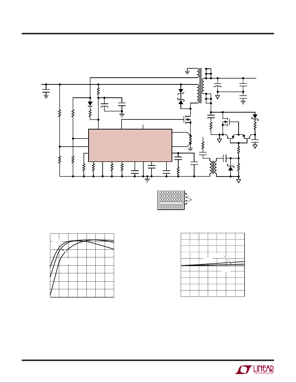
LT3825
TYPICAL APPLICATIO S
+
V
IN
36V TO 72V
2.2µF
100V
BAS21
29.4k
402k
1%
1%
15k
1%
ALL CAPACITORS 25V UNLESS OTHERWISE NOTED
T1: EDFD25-3F3 GAP FOR L
R7
20Ω
V
CC
FB
UVLO
3.01k
1%
PGDLY
tONSYNC
100k12k
= 200µH (i.e., AL = 200nH/T2)
P
PINS 10, 11, 12 TO PINS 7, 8, 9, 4T OF 5 MIL COPPER FOIL
U
48V to 5V at 8A Isolated Supply
47k
1/4W
+
47µF
20V
PG
LT3825
R
ENDLY OSC
CMP
2.1k
100k
1%
47pF
PINS 1 TO 3, 32T OF 2 × 32AWG
PINS 4 TO 5, 11T OF 1 × 32AWG
PINS 1 TO 3, 32T OF 2 × 32AWG
PINS 1 TO 3, 32T OF 2 × 32AWG
0.1µF
SG
SG
GND SFST
P6SMB100A
MBRS1100
SENSE
SENSE
0.22µF
0.1µF
V
C
CMP
Si4490DY
+
–
C
680pF
100k
10nF
T1
4
•
5
•
1
•
3
1nF
10Ω
1/4W
SG
0.03Ω
1W
PA0184
2 MIL
POLYESTER
FILM
7
8
9
+
10
11
12
330Ω
0.1µF
8
5
•
•
BAT54
14
470µF
6TPE470MI
×4
Si7336ADP
×2
FMMT718 FMMT618
15Ω
2.2nF
10k
3825 TA02a
0.1µF
2.2nF
250V
V
OUT
5V
8A
B0540W
47Ω
1µF
+
Efficiency vs Load Current
94
36V
92
IN
90
88
86
84
EFFICIENCY (%)
82
80
78
23 5
1
48V
IN
72V
IN
4
LOAD CURRENT (A)
678
3825 TA02b
Output Regulation vs Load Current
5.25
5.20
5.15
5.10
5.05
5.00
4.95
OUTPUT (V)
4.90
4.85
4.80
4.75
1
3
2
LOAD CURRENT (A)
36V
48V
IN
IN
72V
5
4
6
IN
8
7
3825 TA02c
3825f
28

TYPICAL APPLICATIO S
+
V
IN
36V TO 72V
0.82µF
100V
402k
1%
26.1k
15k
1%
1%
BAS21
3.01k
1%
R7
20Ω
V
FB
UVLO
PGDLY
tONSYNC
100k15k
U
CC
48V to 3.3V at 6A Isolated Supply
47k
1/4W
+
R
47µF
20V
CMP
PG
ENDLY OSC
866Ω
1%
0.1µF
SG
SG
LT3825
GND SFST
62k
47pF
0.22µF
0.1µF
SENSE
SENSE
C
CMP
Si4490DY
+
–
V
C
3.3nF
680pF
10k
T1
PULSE PB2134
4
•
5
•
1
10
•
11
3
12
SG
0.04Ω
1W
330Ω
8
PA0184
14
7
8
9
0.1µF
•
+
B0540W
Si7892DP
5
•
150µF
6TPB150ML
×3
47Ω
FMMT618
FMMT718
2.2nF
BAT54
LT3825
0.1µF
2.2nF
250V
15Ω
10k
3825 TA03a
V
OUT
3.3V
6A
1µF
+
Efficiency vs Load Current Output Regulation vs Load Current
90
36V
IN
88
86
84
EFFICIENCY (%)
82
80
1
72V
IN
48V
IN
2
3
LOAD CURRENT (A)
3.43
3.38
3.33
36V
48V
IN
IN
5
3825 TA03c
3825f
3.28
72V
OUTPUT (V)
3.23
3.18
4
5
6
3825 TA03b
3.13
1
IN
234 6
LOAD CURRENT (A)
29

LT3825
TYPICAL APPLICATIO S
U
48V to 3.3V at 12A Isolated Supply
V
IN
36V TO 72V
2.2µF
100V
92
L1
C1 TO C4
47µF ×3
B0540W
Si7336ADP
•
•
2.2nF
10k
0.1µH
47Ω
Q1
Q2
15Ω
BAT54
+
28.7k
1%
3.01k
1%
402k
1%
UVLO
15k
1%
PGDLY
tONSYNC
100k12k
C1 TO C4: TDK C3225X5R0J476M
C5: SANYO 6TPD470M
L1: VISHAY IHLP2525CZERR10M
T1
•
FB
750Ω 150k
R
CMP
V
CC
ENDLY OSC
BAS21
47k
20Ω
1/4W
+
47µF
SGSGPG
LT3825
GND SFST
47pF
Q1: ZETEX FMMT618
Q2: ZETEX FMMT718
T1: PULSE PA1477NL
Si4490DY
SENSE
SENSE
0.01µF
0.1µF
C
CMP
T1
0.02Ω
1/2W
10nF
10k
1nF
•
•
SG
330Ω
0.1µF
PA0184
100pF
250V
20Ω
+
–
V
C
Efficiency vs Load Current Regulation vs Load Current
3.43
C5
470µF
3825 TA04a
1µF
V
OUT
3.3V
12A
2.2µF
250V
+
90
36V
IN
88
86
84
EFFICIENCY (%)
82
80
78
2
3
48V
72V
IN
5
6
4
LOAD CURRENT (A)
IN
9
7
810
11
3825 TA04b
3.38
36V
3.33
3.28
OUTPUT (V)
3.23
3.18
12
3.13
46810
LOAD CURRENT (A)
48V
72V
IN
IN
IN
122
3825 TA04c
30
3825f

PACKAGE DESCRIPTIO
(.141)
3.58
U
FE Package
16-Lead Plastic TSSOP (4.4mm)
(Reference LTC DWG # 05-08-1663)
Exposed Pad Variation BC
4.90 – 5.10*
(.193 – .201)
3.58
(.141)
16 1514 13 12 11
LT3825
10 9
6.60 ±0.10
4.50 ±0.10
RECOMMENDED SOLDER PAD LAYOUT
0.09 – 0.20
(.0035 – .0079)
NOTE:
1. CONTROLLING DIMENSION: MILLIMETERS
2. DIMENSIONS ARE IN
3. DRAWING NOT TO SCALE
SEE NOTE 4
0.65 BSC
4.30 – 4.50*
(.169 – .177)
0.50 – 0.75
(.020 – .030)
MILLIMETERS
(INCHES)
0.45 ±0.05
2.94
(.116)
1.05 ±0.10
1345678
2
0.25
REF
0° – 8°
0.65
(.0256)
BSC
0.195 – 0.30
(.0077 – .0118)
TYP
4. RECOMMENDED MINIMUM PCB METAL SIZE
FOR EXPOSED PAD ATTACHMENT
*DIMENSIONS DO NOT INCLUDE MOLD FLASH. MOLD FLASH
SHALL NOT EXCEED 0.150mm (.006") PER SIDE
2.94
(.116)
1.10
(.0433)
MAX
0.05 – 0.15
(.002 – .006)
FE16 (BC) TSSOP 0204
6.40
(.252)
BSC
Information furnished by Linear Technology Corporation is believed to be accurate and reliable.
However, no responsibility is assumed for its use. Linear Technology Corporation makes no representation that the interconnection of its circuits as described herein will not infringe on existing patent rights.
3825f
31

LT3825
RELATED PARTS
PART NUMBER DESCRIPTION COMMENTS
LT1424-5 Isolated Flyback Switching Regulator 5V Output Voltage, No Optoisolator Required
LT1424-9 Isolated Flyback Switching Regulator 9V Output Voltage, Regulation Maintained Under Light Loads
LT1425 Isolated Flyback Switching Regulator No Third Winding or Optoisolator Required
LTC1698 Isolated Secondary Synchronous Rectifier Controller Isolated Power Supplies, Contains Voltage Merging, Optocoupler
Driver, Primary Synchronization Circuit
LT1725 General Purpose High Power Isolated Flyback Controller Suitable for Telecom or Offline Input Voltage
LT1737 High Power Isolated Flyback Controller Powered from a DC Supply Voltage
LTC1871 Wide Input Range Current Mode No R
LTC3710 Secondary Side Synchronous Post Regulator Generates a Regulated Auxiliary Output in Isolated DC/DC Converters.
LT3781/LT1698 36V to 72V Input Isolated DC/DC Converter Chipset Synchronous Operation: Overvoltage/Undervoltage Protection,
LTC3803 SOT-23 Flyback Controller Adjustable Slope Compensation, Internal Soft-Start, 200kHz
LTC3806 Synchronous Flyback DC/DC Controller Medium Power Multiple Outputs, 250kHz Soft-Start
No R
is a trademark of Linear Technology Corporation.
SENSE
TM
Controller 50kHz to 1MHz, Boost, Flyback and SEPIC Topology
SENSE
Dual N-Channel MOSFET Synchronous Drivers
10W to 100W Power Supply, 1/2 to 1/4 Brick Footprint
32
Linear Technology Corporation
1630 McCarthy Blvd., Milpitas, CA 95035-7417
(408) 432-1900 ● FAX: (408) 434-0507
●
www.linear.com
3825f
LT 1205 • PRINTED IN USA
© LINEAR TECHNOLOGY CORPORATION 2005
 Loading...