

LT3800
High-Voltage Synchronous
Current Mode Step-Down
FEATURES
■
Wide 4V to 60V Input Voltage Range
■
Output Voltages up to 36V
■
Adaptive Nonoverlap Circuitry Prevents Switch
Shoot-Through
■
Reverse Inductor Current Inhibit for Discontinuous
Operation Improves Efficiency with Light Loads
■
Output Slew Rate Controlled Soft-Start with
Auto-Reset
■
100µA No Load Quiescent Current
■
Low 10µA Current Shutdown
■
1% Regulation Accuracy
■
200kHz Operating Frequency
■
Standard Gate N-Channel Power MOSFETs
■
Current Limit Unaffected by Duty Cycle
■
Reverse Overcurrent Protection
■
16-Lead Thermally Enhanced TSSOP Package
U
APPLICATIO S
■
12V and 42V Automotive and Heavy Equipment
■
48V Telecom Power Supplies
■
Avionics and Industrial Control Systems
■
Distributed Power Converters
U
Controller
DESCRIPTIO
The LT®3800 is a 200kHz fixed frequency high voltage
synchronous current mode step-down switching regulator controller. The IC drives standard gate N-channel power
MOSFETs and can operate with input voltages from 4V to
60V. An onboard regulator provides IC power directly from
V
and provides for output-derived power to minimize V
IN
quiescent current. MOSFET drivers employ an internal
dynamic bootstrap feature, maximizing gate-source “ON”
voltages during normal operation for improved operating
efficiencies. The LT3800 incorporates Burst Mode
tion, which reduces no load quiescent current to under
100µA. Light load efficiencies are also improved through
a reverse inductor current inhibit, allowing the controller
to support discontinuous operation. Both Burst Mode
operation and the reverse-current inhibit features can be
disabled if desired. The LT3800 incorporates a programmable soft-start that directly controls the voltage slew rate
of the converter output for reduced startup surge currents
and overshoot errors. The LT3800 is available in a 16-lead
thermally enhanced TSSOP package.
, LTC and LT are registered trademarks of Linear Technology Corporation.
Burst Mode is a registered trademark of Linear Technology Corporation.
All other trademarks are the property of their respective owners.
Protected by U.S. Patents, including 5481178, 6611131, 6304066, 6498466, 6580258.
®
opera-
IN
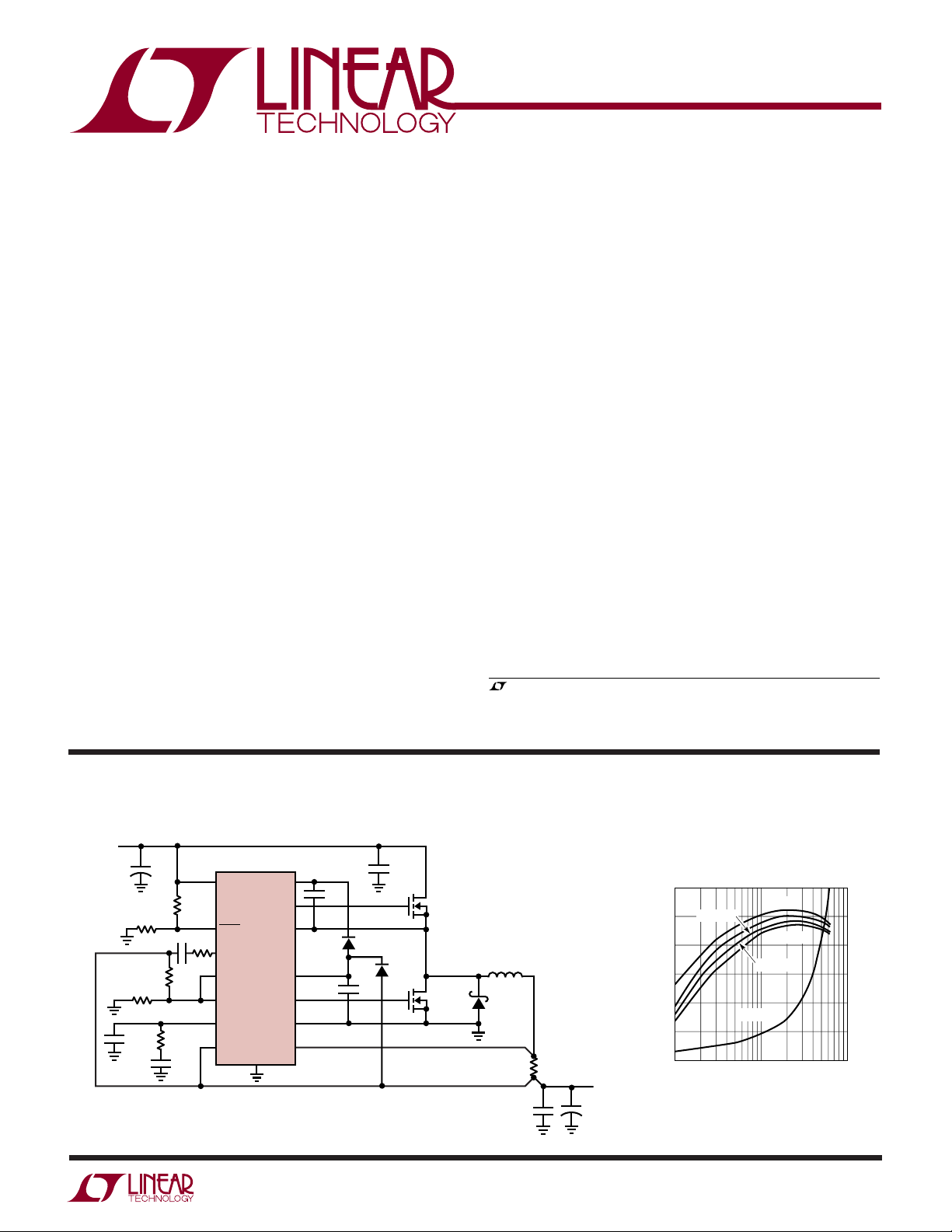
TYPICAL APPLICATIO
12V 75W DC/DC Converter with Reverse Current Inhibit and Input UVLO
V
IN
20V TO 55V
+
82.5k
20k
1%
100pF
56µF
×2
1M
1.5nF
82.5k
680pF
174k
1%
200k
V
IN
LT3800
SHDN
C
SS
BURST_EN
V
FB
V
C
–
SENSE
SGND
BOOST
PGND
SENSE
TG
SW
V
CC
BG
+
U
1µF
BAS19
1µF
1µF
×3
1N4148
Si7850DP
Si7370DP
15µH
B160
10µF
0.015Ω
Efficiency and Power Loss
3800 TA01b
6
5
4
3
2
1
0
10
3800f
POWER LOSS (W)
100
VIN = 36V
95
90
85
EFFICIENCY (%)
80
75
70
V
OUT
12V AT 75W
+
270µF
3800 TA01a
0.1 1
VIN = 24V
VIN = 48V
LOSS (48V)
I
(A)
LOAD
VIN = 60V
1
LT3800
WW
W
U
ABSOLUTE AXI U RATI GS
(Note 1)
Supply Voltages
Input Supply Pin (V
Boosted Supply Pin (BOOST) ................... –0.3V to 80V
Boosted Supply Voltage (BOOST – SW) .. –0.3V to 24V
Boosted Supply Reference Pin (SW) ........... –2V to 65V
Local Supply Pin (VCC) ............................. –0.3V to 24V
Input Voltages
SENSE+, SENSE–...................................... – 0.3V to 40V
SENSE+ – SENSE–......................................... – 1V to 1V
BURST_EN Pin ......................................... –0.3V to 24V
Other Inputs (SHDN, CSS, VFB, VC) .......... –0.3V to 5.0V
Input Currents
SHDN, CSS............................................... –1mA to 1mA
Maximum Temperatures
Operating Junction Temperature Range (Note 2)
LT3800E (Note 3) ............................. –40°C to 125°C
LT3800I ............................................ –40°C to 125°C
Storage Temperature Range ................. –65°C to 150°C
Lead Temperature (Soldering, 10 sec)................. 300°C
) .............................. –0.3V to 65V
IN
UUW
PACKAGE/ORDER I FOR ATIO
TOP VIEW
1
V
IN
2
NC
3
SHDN
4
C
SS
BURST_EN
V
FB
V
C
–
SENSE
16-LEAD PLASTIC TSSOP
T
= 125°C, θJA = 40°C/W, θJC = 10°C/W
JMAX
EXPOSED PAD (PIN 17) IS SGND
MUST BE SOLDERED TO PCB
Consult LTC Marketing for parts specified with wider operating temperature ranges.
5
6
7
8
17
FE PACKAGE
BOOST
16
TG
15
SW
14
NC
13
V
12
CC
BG
11
PGND
10
9
SENSE
+
ORDER PART
NUMBER
LT3800EFE
LT3800IFE
FE PART
MARKING
3800EFE
3800IFE
ELECTRICAL CHARACTERISTICS
The ● denotes the specifications which apply over the full operating
temperature range, otherwise specifications are at TA = 25°C. VIN = 20V, VCC = BOOST = BURST_EN = 10V, SHDN = 2V,
SENSE– = SENSE+ = 10V, SGND = PGND = SW = 0V, CTG = CBG = 3300pF, unless otherwise noted.
SYMBOL PARAMETER CONDITIONS MIN TYP MAX UNITS
V
IN
I
VIN
V
BOOST
I
BOOST
V
CC
Operating Voltage Range (Note 4) ● 460V
Minimum Start Voltage
UVLO Threshold (Falling)
UVLO Hysteresis 670 mV
VIN Supply Current VCC > 9V 20 µA
Burst Mode Current V
V
IN
V
Shutdown Current V
IN
Operating Voltage ● 75 V
Operating Voltage Range (Note 5) V
UVLO Threshold (Rising) V
UVLO Hysteresis V
BOOST Supply Current (Note 6) 1.4 mA
BOOST Burst Mode Current V
BOOST Shutdown Current V
Operating Voltage (Note 5) ● 20 V
Output Voltage
UVLO Threshold (Rising) 6.25 V
UVLO Hysteresis 500 mV
BURST_EN
SHDN
BOOST
BOOST
BOOST
BURST_EN
SHDN
= 0V, VFB = 1.35V 20 µA
= 0V ● 815 µA
– V
SW
– V
SW
– V
SW
= 0V 0.1 µA
= 0V 0.1 µA
● 7.5 V
● 3.65 3.80 3.95 V
● 20 V
5V
0.4 V
● 8.0 8.3 V
2
3800f
LT3800
ELECTRICAL CHARACTERISTICS
temperature range, otherwise specifications are at T
–
SENSE
= SENSE+ = 10V, SGND = PGND = SW = 0V, CTG = CBG = 3300pF, unless otherwise noted.
The ● denotes the specifications which apply over the full operating
= 25°C. VIN = 20V, VCC = BOOST = BURST_EN = 10V, SHDN = 2V,
A
SYMBOL PARAMETER CONDITIONS MIN TYP MAX UNITS
I
V
VCC
SHDN
VCC Supply Current (Note 6) ● 3 3.6 mA
V
Burst Mode Current V
CC
Shutdown Current V
V
CC
Short-Circuit Current
BURST_EN
SHDN
= 0V 80 µA
= 0V 20 µA
● –40 –120 mA
Enable Threshold (Rising) ● 1.30 1.35 1.40 V
Threshold Hysteresis 120 mV
V
SENSE
I
SENSE
f
O
V
FB
I
FB
V
FB(SS)
Common Mode Range ● 036
Current Limit Sense Voltage V
Reverse Protect Sense Voltage V
Reverse Current Offset V
Input Current V
(I
SENSE
+
+ I
–
) 2V < V
SENSE
SENSE
SENSE
BURST_EN
SENSE(CM)
V
SENSE(CM)
+
+
– V
– V
–
SENSE
–
, V
SENSE
= 0V or V
BURST_EN
BURST_EN
= V
= V
● 140 150 175 mV
CC
FB
–150 mV
10 mV
= 0V 0.8 mA
SENSE(CM)
< 3.5V –20 µA
> 4V –0.3 mA
Operating Frequency 190 200 210 kHz
● 175 220 kHz
Error Amp Reference Voltage Measured at VFB Pin 1.224 1.231 1.238 V
● 1.215 1.245 V
Feedback Input Current 25 nA
Soft-Start Disable Voltage VFB Rising 1.185 V
Soft-Start Disable Hysteresis 300 mV
I
g
A
V
I
V
CSS
VC
m
V
C
TG,BG
Soft-Start Capacitor Control Current 2 µA
Error Amp Transconductance ● 275 350 400 µmhos
Error Amp DC Voltage Gain 62 dB
Error Amp Output Range Zero Current to Current Limit 1.2 V
Error Amp Sink/Source Current ±30 µA
Gate Drive Output On Voltage (Note 7) 9.8 V
Gate Drive Output Off Voltage 0.1 V
t
TG,BG
t
TG(OFF)
t
TG(ON)
t
NOL
Gate Drive Rise/Fall Time 10% to 90% or 90% to 10% 50 ns
Minimum Off Time 450 ns
Minimum On Time ● 300 500 ns
Gate Drive Nonoverlap Time TG Fall to BG Rise 200 ns
BG Fall to TG Rise 150 ns
Note 1: Absolute Maximum ratings are those values beyond which the life
of a device may be impaired.
Note 2: This IC includes overtemperature protection that is intended to
protect the device during momentary overload conditions. Junction
temperature will exceed 125°C when overtemperature protection is active.
Continuous operation above the specified maximum operating junction
temperature may impair device reliability.
Note 3: The LT3800E is guaranteed to meet performance specifications
from 0°C to 125°C junction temperature. Specifications over the –40°C to
125°C operating junction temperature range are assured by design,
characterization and correlation with statistical process controls. The
LT3800I is guaranteed over the full –40°C to 125°C operating junction
temperature range.
Note 4: VIN voltages below the start-up threshold (7.5V) are only
supported when V
is externally driven above 6.5V.
CC
Note 5: Operating range dictated by MOSFET absolute maximum gatesource voltage ratings.
Note 6: Supply current specification does not include switch drive
currents. Actual supply currents will be higher.
Note 7: DC measurement of gate drive output “ON” voltage is typically
8.6V. Internal dynamic bootstrap operation yields typical gate “ON”
voltages of 9.8V during standard switching operation. Standard operation
gate “ON” voltage is not tested but guaranteed by design.
3800f
3
LT3800
UW
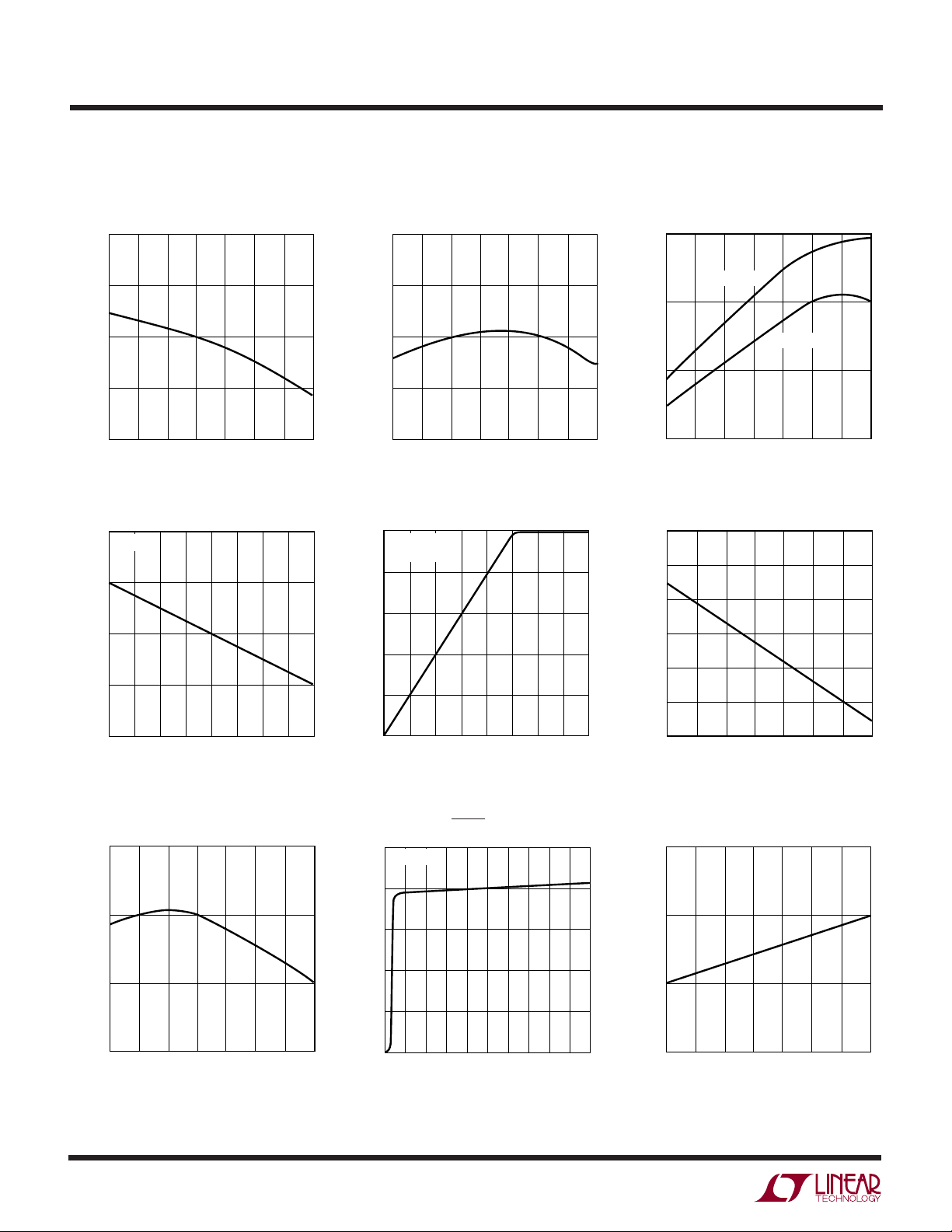
TYPICAL PERFOR A CE CHARACTERISTICS
Shutdown Threshold (Rising)
vs Temperature
1.37
1.36
1.35
1.34
SHUTDOWN THRESHOLD, RISING (V)
(V)
CC
V
1.33
8.05
8.00
7.95
7.90
–50 –25
VCC vs I
TA = 25°C
0 50 12525 75
TEMPERATURE (°C)
CC(LOAD)
100
3800 G01
Shutdown Threshold (Falling)
vs Temperature
1.240
1.235
1.230
1.225
SHUTDOWN THRESHOLD, FALLING (V)
1.220
–50 –25 1000 50 12525 75
TEMPERATURE (°C)
(V)
CC
V
VCC vs V
8
7
6
5
4
ICC = 20mA
= 25°C
T
A
IN
3800 G02
VCC vs Temperature
8.1
ICC = 0mA
8.0
(V)
CC
V
7.9
7.8
–50 –25
05025
ICC = 20mA
TEMPERATURE (°C)
ICC Current Limit vs Temperature
200
175
150
125
100
CURRENT LIMIT (mA)
CC
I
75
75
100
125
3800 G03
7.85
51525
0
10
I
CC(LOAD)
20
(mA)
VCC UVLO Threshold (Rising)
vs Temperature
6.30
6.25
6.20
UVLO THRESHOLD, RISING (V)
CC
V
6.15
–50 –25 100
0 50 12525 75
TEMPERATURE (°C)
3
4
30
35
3800 G04
40
56
8
79 12
V
IN
10 11
(V)
3800 G05
50
–50 –25 1000 50 12525 75
TEMPERATURE (°C)
3800 G06
Error Amp Transconductance
vs Temperature
380
360
340
ERROR AMP TRANSCONDUCTANCE (µmho)
320
–50 –25 1000 50 12525 75
TEMPERATURE (°C)
3800 G08
3800f
3800 G07
(µA)
CC
I
ICC vs V
25
20
15
10
5
0
0
TA = 25°C
246
(SHDN = 0V)
CC
810
VCC (V)
12 14 18
16
20
3800 G12
4
UW
TYPICAL PERFOR A CE CHARACTERISTICS
LT3800
Operating Frequency
I
(SENSE+ + SENSE–)
800
600
(µA)
400
)
–
200
+ SENSE
+
0
(SENSE
I
–200
–400
0 0.5 1.5 2.5 3.5 4.5
1.0 2.0 3.0 4.0
U
V
SENSE(CM)
vs V
SENSE(CM)
TA = 25°C
(V)
5.0
3800 G09
UU
vs Temperature
220
210
200
190
OPERATING FREQUENCY (kHz)
180
–50
–25
TEMPERATURE (°C)
PI FU CTIO S
VIN (Pin 1): Converter Input Supply.
NC (Pin 2): No Connection.
SHDN (Pin 3): Precision Shutdown Pin. Enable threshold
is 1.35V (rising) with 120mV of input hysteresis. When in
shutdown mode, all internal IC functions are disabled. The
precision threshold allows use of the SHDN pin to incorporate UVLO functions. If the SHDN pin is pulled below
0.7V, the IC enters a low current shutdown mode with
I
< 10µA. In low-current shutdown, the IC will sink 20µA
VIN
from the VCC pin until that local supply has collapsed.
Typical pin input bias current is <10nA and the pin is
internally clamped to 6V.
CSS (Pin 4): Soft-Start AC Coupling Capacitor Input.
Connect capacitor (CSS) in series with a 200k resistor from
pin to converter output (V
up output voltage slew rate (∆V
sponds to 2µA average current through the soft-start
coupling capacitor. The capacitor value for a desired
output startup slew rate follows the relation:
CSS = 2µA/(∆V
OUT
/∆t)
Shorting this pin to SGND disables the soft-start function.
). Controls converter start-
OUT
/∆t). Slew rate corre-
OUT
Error Amp Reference
vs Temperature
1.232
1.231
1.230
1.229
ERROR AMP REFERENCE (V)
1.228
1.227
1000 50 12525 75
3800 G10
–50 –25 1000 50 12525 75
TEMPERATURE (°C)
3800 G11
BURST_EN (Pin 5): Burst Mode Operation Enable Pin.
This pin also controls reverse-inhibit mode of operation.
When the pin voltage is below 0.5V, Burst Mode operation
and reverse-current inhibit functions are enabled. When
the pin voltage is above 0.5V, Burst Mode operation is
disabled, but reverse-current inhibit operation is maintained. DC/DC converters operating with reverse-current
inhibit operation (BURST_EN = VFB) have a 1mA minimum
load requirement. Reverse-current inhibit is disabled when
the pin voltage is above 2.5V. This pin is typically shorted
to ground to enable Burst Mode operation and reversecurrent inhibit, shorted to VFB to disable Burst Mode
operation while enabling reverse-current inhibit, and connected to VCC pin to disable both functions. See Applications Information section.
VFB (Pin 6): Error Amplifier Inverting Input. The
noninverting input of the error amplifier is connected to an
internal 1.231V reference. Desired converter output voltage (V
) is programmed by connecting a resistive
OUT
divider from the converter output to the VFB pin. Values for
the resistor connected from V
to VFB (R2) and the
OUT
resistor connected from VFB to ground (R1) can be calculated via the following relationship:
RR
21
•
V
⎛
⎜
⎝
1 231
.
OUT
⎞
1=
–
⎟
⎠
3800f
5

LT3800
U
UU
PI FU CTIO S
The VFB pin input bias current is 25nA, so use of extremely
high value feedback resistors could cause a converter
output that is slightly higher than expected. Bias current
error at the output can be estimated as:
∆V
OUT(BIAS)
(Pin 7): Error Amplifier Output. The voltage on the V
V
C
pin corresponds to the maximum (peak) switch current
per oscillator cycle. The error amplifier is typically configured as an integrator by connecting an RC network from
this pin to ground. This network creates the dominant pole
for the converter voltage regulation feedback loop. Specific integrator characteristics can be configured to optimize transient response. Connecting a 100pF or greater
high frequency bypass capacitor from this pin to ground
is also recommended. When Burst Mode operation is
enabled (see Pin 5 description), an internal low impedance
clamp on the VC pin is set at 100mV below the burst
threshold, which limits the negative excursion of the pin
voltage. Therefore, this pin cannot be pulled low with a
low-impedance source. If the VC pin must be externally
manipulated, do so through a 1kΩ series resistance.
SENSE– (Pin 8): Negative Input for Current Sense Amplifier. Sensed inductor current limit set at ±150mV across
SENSE inputs.
SENSE+ (Pin 9): Positive Input for Current Sense Amplifier. Sensed inductor current limit set at ±150mV across
SENSE inputs.
= 25nA • R2
C
PGND (Pin 10): High Current Ground Reference for Synchronous Switch. Current path from pin to negative terminal of V
BG (Pin 11): Synchronous Switch Gate Drive Output.
VCC (Pin 12): Internal Regulator Output. Most IC func-
tions are powered from this pin. Driving this pin from an
external source reduces VIN pin current to 20µA. This pin
is decoupled with a low ESR 1µF capacitor to PGND.
In shutdown mode, this pin sinks 20µA until the pin
voltage is discharged to 0V. See Typical Performance
Characteristics.
NC (Pin 13): No Connection.
SW (Pin 14): Reference for V
Current Return for Bootstrapped Switch.
TG (Pin 15): Bootstrapped Switch Gate Drive Output.
BOOST (Pin 16): Bootstrapped Supply – Maximum Oper-
ating Voltage (Ground Referred) to 75V. This pin is
decoupled with a low ESR 1µF capacitor to pin SW. The
voltage on the decoupling capacitor is refreshed through
a rectifier from either VCC or an external source.
Exposed Package Backside (SGND) (Pin 17): Low Noise
Ground Reference. SGND connection is made through the
exposed lead frame on back of TSSOP package which
must be soldered to the PCB ground.
decoupling capacitor must not corrupt SGND.
CC
Supply and High
BOOST
6
3800f

LT3800
U
U
W
FU CTIO AL DIAGRA
V
IN
UVLO
(<4V)
1
V
IN
8V
REG
+
–
3
SHDN
BURST_EN
5
FEEDBACK
REFERENCE
1.231V
+
–
+
3.8V
REG
V
CC
UVLO
(<6V)
INTERNAL
SUPPLY RAIL
BST
UVLO
DRIVE
CONTROL
NOL
SWITCH
DRIVE
LOGIC
CONTROL
DRIVE
CONTROL
SYNCHRONOUS
SWITCH DRIVER
BOOSTED
SWITCH
DRIVER
BOOST
16
TG
15
SW
14
V
12
CC
BG
11
PGND
10
V
FB
V
C
SS
GND
–
SQ
+
OSCILLATOR
SLOPE COMP
GENERATOR
REVERSE
CURRENT
INHIBIT
160mV
–
10mV
Q
R
S
+
+
SENSE
9
–
SENSE
8
+
6
–+
g
SOFT-START
ENABLE
+
m
0.5V
1V
ERROR
AMP
7
C
DISABLE/BURST
–
R
CURRENT
–
+
SENSE
COMPARATOR
–
–
Burst Mode
1.185V
2µA
4
OPERATION
–
+
17
3800 FD
3800f
7

LT3800
U
WUU
APPLICATIO S I FOR ATIO
Overview
The LT3800 is a high input voltage range step-down
synchronous DC/DC converter controller IC that uses a
200kHz constant frequency, current mode architecture
with external N-channel MOSFET switches.
The LT3800 has provisions for high efficiency, low load
operation for battery-powered applications. Burst Mode
operation reduces total average input quiescent currents
to 100µA during no load conditions. A low current shutdown
mode can also be activated, reducing quiescent current to
<10µA. Burst Mode operation can be disabled if desired.
The LT3800 also employs a reverse-current inhibit feature, allowing increased efficiencies during light loads
through nonsynchronous operation. This feature disables
the synchronous switch if inductor current approaches
zero. If full time synchronous operation is desired, this
feature can be disabled.
Much of the LT3800’s internal circuitry is biased from an
internal linear regulator. The output of this regulator is the
VCC pin, allowing bypassing of the internal regulator. The
associated internal circuitry can be powered from the
output of the converter, increasing overall converter efficiency. Using externally derived power also eliminates the
IC’s power dissipation associated with the internal VIN to
VCC regulator.
threshold is not obtained for the entire oscillator cycle, the
switch driver is disabled at the end of the cycle for 450ns.
This minimum off-time mode of operation assures regeneration of the BOOST bootstrapped supply.
Power Requirements
The LT3800 is biased using a local linear regulator to
generate internal operational voltages from the VIN pin.
Virtually all of the circuitry in the LT3800 is biased via an
internal linear regulator output (V
with a low ESR 1µF capacitor to PGND.
The V
is ample voltage on the VIN pin. The VCC regulator has
approximately 1V of dropout, and will follow the VIN pin
with voltages below the dropout threshold.
The LT3800 has a start-up requirement of VIN > 7.5V. This
assures that the onboard regulator has ample headroom
to bring the VCC pin above its UVLO threshold. The V
regulator can only source current, so forcing the VCC pin
above its 8V regulated voltage allows use of externally
derived power for the IC, minimizing power dissipation in
the IC. Using the onboard regulator for start-up, then
deriving power for VCC from the converter output maximizes conversion efficiencies and is common practice. If
VCC is maintained above 6.5V using an external source, the
LT3800 can continue to operate with VIN as low as 4V.
regulator generates an 8V output provided there
CC
). This pin is decoupled
CC
CC
Theory of Operation (See Block Diagram)
The LT3800 senses converter output voltage via the V
pin. The difference between the voltage on this pin and an
internal 1.231V reference is amplified to generate an error
voltage on the VC pin which is, in turn, used as a threshold
for the current sense comparator.
During normal operation, the LT3800 internal oscillator
runs at 200kHz. At the beginning of each oscillator cycle,
the switch drive is enabled. The switch drive stays enabled
until the sensed switch current exceeds the VC derived
threshold for the current sense comparator and, in turn,
disables the switch driver. If the current comparator
FB
8
The LT3800 operates with 3mA quiescent current from the
VCC supply. This current is a fraction of the actual V
quiescent currents during normal operation. Additional
current is produced from the MOSFET switching currents
for both the boosted and synchronous switches and are
typically derived from the V
Because the LT3800 uses a linear regulator to generate
VCC, power dissipation can become a concern with high
VIN voltages. Gate drive currents are typically in the range
of 5mA to 15mA per MOSFET, so gate drive currents can
create substantial power dissipation. It is advisable to
derive VCC and V
whenever possible.
BOOST
supply.
CC
power from an external source
CC
3800f

WUUU
V
OUT
1µF
B0520
B0520
1µF
Si1555DL
LT3800
V
CC
BG
V
OUT
1µF
B0520
B0520
1µF
1µF
Si1555DLSi1555DL
LT3800
V
CC
BG
B0520
3800 AI01
APPLICATIO S I FOR ATIO
LT3800
The onboard VCC regulator will provide gate drive power for
start-up under all conditions with total MOSFET gate charge
loads up to 180nC. The regulator can operate the LT3800
continuously, provided the VIN voltage and/or MOSFET gate
charge currents do not create excessive power dissipation
in the IC. Safe operating conditions for continuous regulator use are shown in Figure 1. In applications where these
conditions are exceeded, VCC must be derived from an
external source after start-up.
70
60
50
(V)
40
IN
V
30
SAFE
20
OPERATING
CONDITIONS
10
0
Figure 1. VCC Regulator Continuous Operating Conditions
50 100 150 200
TOTAL FET GATE CHARGE (nC)
3800 F01
Charge Pump Doubler
Charge Pump Tripler
Inductor Auxiliary Winding
In LT3800 converter applications with output voltages in
the 9V to 20V range, back-feeding VCC and V
the converter output is trivial, accomplished by connecting diodes from the output to these supply pins. Deriving
these supplies from output voltages greater than 20V will
require additional regulation to reduce the feedback voltage. Outputs lower than 9V will require step-up techniques
to increase the feedback voltage to something greater than
the 8V VCC regulated output. Low power boost switchers
are sometimes used to provide the step-up function, but
a simple charge-pump can perform this function in many
instances.
BOOST
from
LT3800
SW
V
TG
BG
N
CC
•
V
OUT
•
3800 AI04
3800f
9

LT3800
WUUU
APPLICATIO S I FOR ATIO
Burst Mode
The LT3800 employs low current Burst Mode functionality
to maximize efficiency during no load and low load conditions. Burst Mode operation is enabled by shorting the
BURST_EN pin to SGND. Burst Mode operation can be
disabled by shorting BURST_EN to either V
When the required switch current, sensed via the V
or VCC.
FB
pin
C
voltage, is below 15% of maximum, the Burst Mode
operation is employed and that level of sense current is
latched onto the IC control path. If the output load requires
less than this latched current level, the converter will
overdrive the output slightly during each switch cycle.
This overdrive condition is sensed internally and forces
the voltage on the VC pin to continue to drop. When the
voltage on VC drops 150mV below the 15% load level,
switching is disabled and the LT3800 shuts down most of
its internal circuitry, reducing total quiescent current to
100µA. When the converter output begins to fall, the VC pin
voltage begins to climb. When the voltage on the VC pin
climbs back to the 15% load level, the IC returns to normal
operation and switching resumes. An internal clamp on
the VC pin is set at 100mV below the switch disable
threshold, which limits the negative excursion of the pin
voltage, minimizing the converter output ripple during
Burst Mode operation.
During Burst Mode operation, VIN pin current is 20µA and
VCC current is reduced to 80µA. If no external drive is
provided for V
V
pin, giving a total VIN current of 100µA. Burst current
IN
, all VCC bias currents originate from the
CC
can be reduced further when VCC is driven using an output
derived source, as the V
component of VIN current is
CC
then reduced by the converter buck ratio.
Reverse-Current Inhibit
The LT3800 contains a reverse-current inhibit feature to
maximize efficiency during light load conditions. This
mode of operation allows discontinuous operation, and is
sometimes referred to as “pulse-skipping” mode. Refer to
Figure 2.
This feature is enabled with Burst Mode operation, and can
also be enabled while Burst Mode operation is disabled by
shorting the BURST_EN pin to V
FB
.
When reverse-current inhibit is enabled, the LT3800 sense
amplifier detects inductor currents approaching zero and
disables the synchronous switch for the remainder of the
switch cycle. If the inductor current is allowed to go
negative before the synchronous switch is disabled, the
switch node could inductively kick positive with a high
dv/dt. The LT3800 prevents this by incorporating a 10mV
positive offset at the sense inputs.
10
DECREASING
LOAD
CURRENT
PULSE SKIP MODE
I
L
FORCED CONTINUOUS
I
L
Figure 2. Inductor Current vs Mode
3800 F02
3800f

WUUU
APPLICATIO S I FOR ATIO
LT3800
With the reverse-current inhibit feature enabled, an LT3800
converter will operate much like a nonsynchronous
converter during light loads. Reverse-current inhibit reduces resistive losses associated with inductor ripple
currents, which improves operating efficiencies during
light-load conditions.
An LT3800 DC/DC converter that is operating in reverseinhibit mode has a minimum load requirement of 1mA
(BURST_EN = V
). Since most applications use output-
FB
generated power for the LT3800, this requirement is met
by the bias currents of the IC, however, for applications
that do not derive power from the output, this requirement is easily accomplished by using a 1.2k resistor
connected from VFB to ground as one of the converter
output voltage programming resistors (R1). There are no
minimum load restrictions when in Burst Mode operation
(BURST_EN < 0.5V) or continuous conduction mode
(BURST_EN > 2.5V).
Soft-Start
The LT3800 incorporates a programmable soft-start function to control start-up surge currents, limit output overshoot and for use in supply sequencing. The soft-start
function directly monitors and controls output voltage
slew rate during converter start-up.
As the output voltage of the converter rises, the soft-start
circuit monitors δV/δt current through a coupling capacitor and adjusts the voltage on the VC pin to maintain an
average value of 2µA. The soft-start function forces the
programmed slew rate while the converter output rises to
95% regulation, which corresponds to 1.185V on the V
FB
pin. Once 95% regulation is achieved, the soft-start circuit
is disabled. The soft-start circuit will re-enable when the V
FB
pin drops below 70% regulation, which corresponds to
300mV of control hysteresis on the VFB pin, which allows
for a controlled recovery from a ‘brown-out’ condition.
The desired soft-start rise time (tSS) is programmed via
a programming capacitor C
, using a value that
SS1
corresponds to 2µA average current during the soft-start
interval. This capacitor value follows the relation:
6
–
2
•t
E
C
SS1
=
V
SS
OUT
RSS is typically set to 200k for most applications.
C
SS1
R
SS
V
OUT
A
C
LT3800
SS
3800 AI06
Considerations for Low Voltage Output Applications
The LT3800 CSS pin biases to 220mV during the soft-start
cycle, and this voltage is increased at network node “A” by
the 2µA signal current through RSS, so the output has to
reach this value before the soft-start function is engaged.
The value of this output soft-start start-up voltage offset
(V
OUT(SS)
V
) follows the relation:
OUT(SS)
= 220mV + RSS • 2E
–6
which is typically 0.64V for RSS = 200k.
In some low voltage output applications, it may be desirable to reduce the value of this soft-start start-up voltage
offset. This is possible by reducing the value of RSS. With
reduced values of RSS, the signal component caused by
voltage ripple on the output must be minimized for proper
soft-start operation.
Peak-to-peak output voltage ripple (∆V
posed on node “A” through the capacitor C
) will be im-
OUT
. The value
SS1
of RSS can be set using the following equation:
V
∆
=
1.3E
OUT
–6
R
SS
It is important to use low ESR output capacitors for
LT3800 voltage converter designs to minimize this ripple
voltage component. A design with an excessive ripple
component can be evidenced by observing the VC pin
during the start cycle.
3800f
11

LT3800
WUUU
APPLICATIO S I FOR ATIO
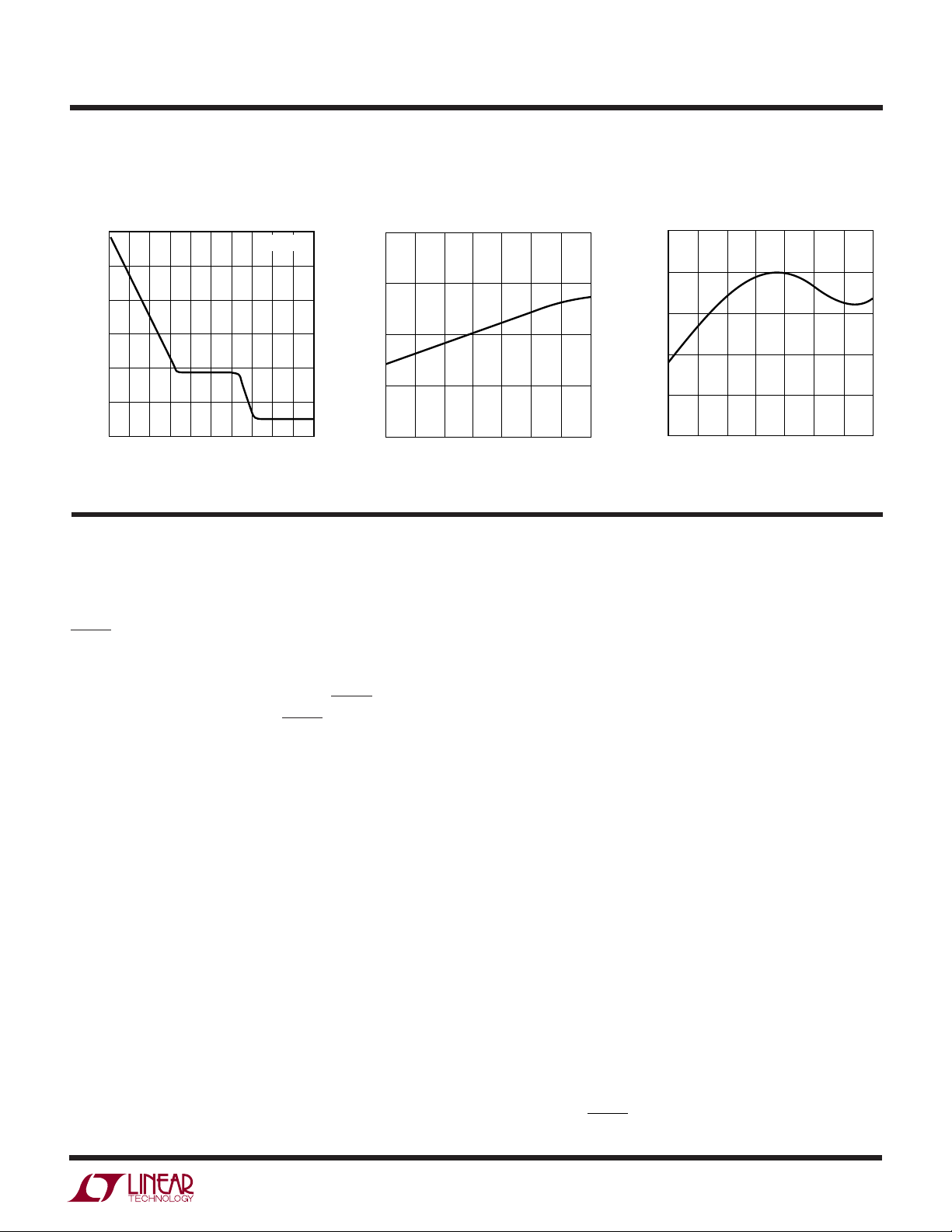
Soft-Start Characteristic Showing Excessive Ripple Component
V
OUT
V
OUT(SS)
V(VC)
250µs/DIV
3800 AI07
The soft-start cycle should be evaluated to verify that the
reduced RSS value allows operation without excessive
modulation of the VC pin before finalizing the design.
If the VC pin has an excessive ripple component during the
soft-start cycle, converter output ripple should be reduced
or RSS increased. Reduction in converter output ripple is
typically accomplished by increasing output capacitance
and/or reducing output capacitor ESR.
External Current Limit Foldback Circuit
An additional start-up voltage offset can occur during the
period before the LT3800 soft-start circuit becomes active. Before the soft-start circuit throttles back the VC pin
in response to the rising output voltage, current as high as
the peak programmed current limit (I
) can flow in the
MAX
inductor. Switching will stop once the soft-start circuit
takes hold and reduces the voltage on the VC pin, but the
output voltage will continue to increase as the stored
energy in the inductor is transferred to the output capacitor. With I
ing-edge rise on V
flowing in the inductor, the resulting lead-
MAX
due to energy stored in the inductor
OUT
follows the relationship:
∆ =
VI
OUT MAX
⎛
•
⎜
⎝
C
L
OUT
/12
⎞
⎟
⎠
Desirable Soft-Start Characteristic
V
OUT
V
OUT(SS)
V(VC)
250µs/DIV
Inductor current typically doesn’t reach I
3800 AI08
in the few
MAX
cycles that occur before soft-start becomes active, but can
with high input voltages or small inductors, so the above
relation is useful as a worst-case scenario.
This energy transfer increase in output voltage is typically
small, but for some low voltage applications with relatively
small output capacitors, it can become significant. The
voltage rise can be reduced by increasing output capacitance, which puts additional limitations on C
for these
OUT
low voltage supplies. Another approach is to add an
external current limit foldback circuit which reduces the
value of I
during start-up.
MAX
An external current limit foldback circuit can be easily
incorporated into an LT3800 DC/DC converter application
by placing a 1N4148 diode and a 47k resistor from the
converter output (V
the peak current to 0.25 • I
) to the LT3800’s VC pin. This limits
OUT
MAX
when V
= 0V. A current
OUT
limit foldback circuit also has the added advantage of
providing a reduced output current in the DC/DC converter
during short-circuit fault conditions, so a foldback circuit
may be useful even if the soft-start function is disabled.
If the soft-start circuit is disabled by shorting the CSS pin
to ground, the external current limit fold-back circuit must
be modified by adding an additional diode and resistor.
The 2-diode, 2-resistor network shown also provides
0.25 • I
MAX
when V
OUT
= 0V.
12
3800f

WUUU
APPLICATIO S I FOR ATIO
LT3800
Current Limit Foldback Circuit for
Applications That Use Soft-Start
V
C
1N4148
47k
V
3800 AI09
OUT
Adaptive Nonoverlap (NOL) Output Stage
The FET driver output stages implement adaptive
nonoverlap control. This feature maintains a constant
dead time, preventing shoot-through switch currents,
independent of the type, size or operating conditions of the
external switch elements.
Each of the two switch drivers contains a NOL control
circuit, which monitors the output gate drive signal of the
other switch driver. The NOL control circuits interrupt the
“turn on” command to their associated switch driver until
the other switch gate is fully discharged.
Antislope Compensation
Most current mode switching controllers use slope compensation to prevent current mode instability. The LT3800
is no exception. A slope-compensation circuit imposes an
artificial ramp on the sensed current to increase the rising
slope as duty cycle increases. Unfortunately, this additional ramp corrupts the sensed current value, reducing
the achievable current limit value by the same amount as
the added ramp represents. As such, current limit is
typically reduced as duty cycles increase. The LT3800
contains circuitry to eliminate the current limit reduction
typically associated with slope compensation. As the
slope-compensation ramp is added to the sensed current,
a similar ramp is added to the current limit threshold
reference. The end result is that current limit is not
compromised, so a LT3800 converter can provide full
power regardless of required duty cycle.
Alternative Current Limit Foldback Circuit for Applications That
Have Soft-Start Disabled
V
C
1N4148
1N4148
39k
27k
3800 AI10
V
OUT
Shutdown
The LT3800 SHDN pin uses a bandgap generated reference threshold of 1.35V. This precision threshold allows
use of the SHDN pin for both logic-level controlled applications and analog monitoring applications such as power
supply sequencing.
The LT3800 operational status is primarily controlled by a
UVLO circuit on the VCC regulator pin. When the IC is
enabled via the SHDN pin, only the VCC regulator is
enabled. Switching remains disabled until the UVLO threshold is achieved at the VCC pin, when the remainder of the
IC is enabled and switching commences.
Because an LT3800 controlled converter is a power transfer device, a voltage that is lower than expected on the
input supply could require currents that exceed the sourcing capabilities of that supply, causing the system to lock
up in an undervoltage state. Input supply start-up protection can be achieved by enabling the SHDN pin using a
resistive divider from the VIN supply to ground. Setting the
divider output to 1.35V when that supply is at an adequate
voltage prevents an LT3800 converter from drawing large
currents until the input supply is able to provide the
required power. 120mV of input hysteresis on the SHDN
pin allows for almost 10% of input supply droop before
disabling the converter.
3800f
13

LT3800
∆ =
⎛
⎝
⎜
⎞
⎠
⎟
I
V
V
V
fL
L
OUT
IN
OUT
O
1– •
•
WUUU
APPLICATIO S I FOR ATIO
Programming LT3800 VIN UVLO
V
IN
R
R
The UVLO voltage, V
B
A
IN(UVLO)
LT3800
3
SHDN
SGND
3800 AI02
17
, is set using the following
relation:
RR
= •
AB
VV
IN UVLO
()
.
135
–.
135
V
If additional hysteresis is desired for the enable function,
an external positive feedback resistor can be used from the
LT3800 regulator output.
The shutdown function can be disabled by connecting the
SHDN pin to VIN through a large value pull-up resistor.
This pin contains a low impedance clamp at 6V, so the
SHDN pin will sink current from the pull-up resistor (RPU):
VV
–6
I
SHDN
IN
=
R
PU
Because this arrangement will pull the SHDN pin to the 6V
clamp voltage, it will violate the 5V absolute maximum
voltage rating of the pin. This is permitted, however, as
long as the absolute maximum input current rating of 1mA
is not exceeded. Input SHDN pin currents of <100µA are
recommended; a 1MΩ or greater pull-up resistor is typically used for this configuration.
Inductor Selection
The primary criterion for inductor value selection in LT3800
applications is ripple current created in that inductor.
Basic design considerations for ripple current are output
voltage ripple, and the ability of the internal slope compensation waveform to prevent current mode instability. Once
the value is determined, an inductor must also have a
saturation current equal to or exceeding the maximum
peak current in the inductor.
Ripple current (∆I
) in an inductor for a given value (L) can
L
be approximated using the relation:
The typical range of values for ∆I is 20% to 40% of
I
OUT(MAX)
, where I
OUT(MAX)
is the maximum converter
output load current. Ripple currents in this range typically
yield a good design compromise between inductor performance versus inductor size and cost, and values in this
range are generally a good starting point. A starting point
inductor value can thus be determined using the relation:
LV
=
OUT
⎛
1
–
⎜
⎝
•
fI
03
•.•
O OUT MAX
V
OUT
V
IN
⎞
⎟
⎠
()
Use of smaller inductors increase output ripple currents,
requiring more capacitance on the converter output. Also,
with converter operation with duty cycles greater than
50%, the slope compensation criterion, described later,
must be met. Designing for smaller ripple currents requires larger inductor values, which can increase converter cost and/or footprint.
14
3800f

WUUU
APPLICATIO S I FOR ATIO
LT3800
Some magnetics vendors specify a volt-second product in
their data sheet. If they do not, consult the vendor to make
sure the specification is not being exceeded by your
design. The required volt-second product is calculated as
follows:
Volt
- Second
OUT
f
O
⎛
•–1
⎜
⎝
V
≥
V
OUT
V
IN
⎞
⎟
⎠
Magnetics vendors specify either the saturation current,
the RMS current, or both. When selecting an inductor
based on inductor saturation current, the peak current
through the inductor, I
OUT(MAX)
+ (∆I/2), is used. When
selecting an inductor based on RMS current the maximum
load current, I
OUT(MAX)
, is used.
The requirement for avoiding current mode instability is
keeping the rising slope of sensed inductor ripple current
(S1) greater than the falling slope (S2). During continuouscurrent switcher operation, the rising slope of the current
waveform in the switched inductor is less than the falling
slope when operating at duty cycles (DC) greater than 50%.
To avoid the instability condition during this operation, a
false signal is added to the sensed current, increasing the
perceived rising slope. To prevent current mode instability, the slope of this false signal (Sx) must be sufficient such
that the sensed rising slope exceeds the falling slope, or
S1 + Sx ≥ S2. This leads to the following relations:
Sx ≥ S2 (2DC – 1)/DC
where:
S2 ~ V
OUT
/L
Solving for L yields a relation for the minimum inductance
that will satisfy slope compensation requirements:
duty cycle, to generate an equivalent slope of at least
1E5 • I
A/sec, where I
LIMIT
is the programmed con-
LIMIT
verter current limit. Current limit is programmed by using
a sense resistor (RS) such that I
= 150mV/RS, so the
LIMIT
equation for the minimum inductance to meet the current
mode instability criterion can be reduced to:
L
= (5E–5)(V
MIN
For example, with V
L
= (5E–5)(5)(0.02) = 5µH
MIN
)(RS)
OUT
= 5V and RS = 20mΩ:
OUT
After calculating the minimum inductance value, the voltsecond product, the saturation current and the RMS
current for your design, an off the shelf inductor can be
selected from a magnetics vendor. A list of magnetics
vendors can be found at http://www.linear.com/ezone/
vlinks or by contacting the Linear Technology Applications
department.
Output Voltage Programming
Output voltage is programmed through a resistor feedback network to VFB (Pin 6) on the LT3800. This pin is the
inverting input of the error amplifier, which is internally
referenced to 1.231V. The divider is ratioed to provide
1.231V at the VFB pin when the output is at its desired
value. The output voltage is thus set following the relation:
RR
21
⎛
•
⎜
⎝
OUT
1 231
.
⎞
1=
–
⎟
⎠
V
when an external resistor divider is connected to the
output as shown.
Programming LT3800 Output Voltage
DC
–
LV
= •
MIN OUT
21
DC Sx
•
The LT3800 maximizes available dynamic range using a
slope compensation generator that continuously increases
the additional signal slope as duty cycle increases. The
slope compensation waveform is calibrated at an 80%
LT3800
SGND
17
V
OUT
R2
6
V
FB
R1
3800 AI03
3800f
15

LT3800
WUUU
APPLICATIO S I FOR ATIO
Power MOSFET Selection
I
MAIN
= (I
LOAD
)(DC)
External N-channel MOSFET switches are used with the
LT3800. The positive gate-source drive voltage of the
LT3800 for both switches is roughly equivalent to the V
CC
supply voltage, for use of standard threshold MOSFETs.
Selection criteria for the power MOSFETs include the “ON”
resistance (R
capacitance (C
), total gate charge (QG), reverse transfer
DS(ON)
), maximum drain-source voltage (V
RSS
DSS
)
and maximum current.
The power FETs selected must have a maximum operating
V
exceeding the maximum VIN. VGS voltage maximum
DSS
must exceed the VCC supply voltage.
Total gate charge (QG) is used to determine the FET gate
drive currents required. QG increases with applied gate
voltage, so the QG for the maximum applied gate voltage
must be used. A graph of QG vs. VGS is typically provided
in MOSFET datasheets.
In a configuration where the LT3800 linear regulator is
providing VCC and V
currents, the VCC 8V output
BOOST
voltage can be used to determine QG. Required drive
current for a given FET follows the simple relation:
I
= Q
GATE
Q
is the total FET gate charge for VGS = 8V, and f0 =
G(8V)
G(8V)
• f
O
operating frequency. If these currents are externally derived by backdriving VCC, use the backfeed voltage to
determine QG. Be aware, however, that even in a backfeed
configuration, the drive currents for both boosted and
synchronous FETs are still typically supplied by the LT3800
internal VCC regulator during start-up. The LT3800 can
start using FETs with a combined Q
Once voltage requirements have been determined, R
up to 180nC.
G(8V)
DS(ON)
can be selected based on allowable power dissipation and
required output current.
In an LT3800 buck converter, the average inductor current
is equal to the DC load current. The average currents
through the main (bootstrapped) and synchronous
(ground-referred) switches are:
I
SYNC
The R
= (I
DS(ON)
)(1 – DC)
LOAD
required for a given conduction loss can be
calculated using the relation:
P
LOSS
= I
SWITCH
2
• R
DS(ON)
In high voltage applications (VIN > 20V), the main switch
is required to slew very large voltages. MOSFET transition
losses are proportional to V
2
and can become the
IN
dominant power loss term in the main switch. This transition loss takes the form:
PTR ≈ (k)(VIN)2(I
SWITCH
)(C
RSS
)(fO)
where k is a constant inversely related to the gate drive
current, approximated by k = 2 in LT3800 applications,
and I
SWITCH
is the converter output current. The power
loss terms for the switches are thus:
P
MAIN
P
SYNC
= (DC)(I
SWITCH
2(VIN)2(I
= (1 – DC)(I
)2(1 + d)(R
SWITCH
SWITCH
)(C
RSS
)(fO)
)2(1 + d)(R
DS(ON)
DS(ON)
) +
)
The (1 + d) term in the above relations is the temperature
dependency of R
normalized R
DS(ON)
, typically given in the form of a
DS(ON)
vs Temperature curve in a MOSFET
data sheet.
The C
and it is often advantageous to use a FET with a higher V
term is typically smaller for higher voltage FETs,
RSS
DS
rating to minimize transition losses at the expense of
additional R
DS(ON)
losses.
In some applications, parasitic FET capacitances couple
the negative going switch node transient onto the bottom
gate drive pin of the LT3800, causing a negative voltage in
excess of the Absolute Maximum Rating to be imposed on
that pin. Connection of a catch Schottky diode from this
pin to ground will eliminate this effect. A 1A current rating
is typically sufficient for the diode.
16
3800f

WUUU
APPLICATIO S I FOR ATIO
LT3800
Input Capacitor Selection
The large currents typical of LT3800 applications require
special consideration for the converter input and output
supply decoupling capacitors. Under normal steady state
buck operation, the source current of the main switch
MOSFET is a square wave of duty cycle V
OUT/VIN
. Most of
this current is provided by the input bypass capacitor. To
prevent large input voltage transients and avoid bypass
capacitor heating, a low ESR input capacitor sized for the
maximum RMS current must be used. This maximum
capacitor RMS current follows the relation:
2
RMS
= I
MAX
/2.
I
RMS
IVVV
()
MAX OUT IN OUT
=
–
()
V
IN
which peaks at a 50% duty cycle, when I
The bulk capacitance is calculated based on an acceptable
maximum input ripple voltage, ∆VIN, which follows the
relation:
V
OUT
V
CI
IN BULK OUT MAX
() ()
=
•
Vf
∆
IN
•
IN O
∆V is typically on the order of 100mV to 200mV. Aluminum electrolytic capacitors are a good choice for high
voltage, bulk capacitance due to their high capacitance per
unit area.
The capacitor voltage rating must be rated greater than
V
IN(MAX)
. The combination of aluminum electrolytic capacitors and ceramic capacitors is a common approach to
meeting supply input capacitor requirements. Multiple
capacitors are also commonly paralleled to meet size or
height requirements in a design.
Capacitor ripple current ratings are often based on only
2000 hours (three months) lifetime; it is advisable to
derate either the ESR or temperature rating of the capacitor for increased MTBF of the regulator.
Output Capacitor Selection
The output capacitor in a buck converter generally has
much less ripple current than the input capacitor. Peak-topeak ripple current is equal to that in the inductor (∆IL),
typically a fraction of the load current. C
is selected to
OUT
reduce output voltage ripple to a desirable value given an
expected output ripple current. Output ripple (∆V
OUT
) is
approximated by:
≈ ∆IL(ESR + [(8)(fO) • C
∆V
OUT
where f
∆V
= operating frequency.
O
increases with input voltage, so the maximum
OUT
OUT
]–1)
operating input voltage should be used for worst-case
calculations. Multiple capacitors are often paralleled to
meet ESR requirements. Typically, once the ESR requirement is satisfied, the capacitance is adequate for filtering
and has the required RMS current rating. An additional
ceramic capacitor in parallel is commonly used to reduce
the effect of parasitic inductance in the output capacitor,
which reduces high frequency switching noise on the
converter output.
Increasing inductance is an option to reduce ESR requirements. For extremely low ∆V
an additional LC filter
OUT,
stage can be added to the output of the supply. Application Note 44 has information on sizing an additional
output LC filter.
Layout Considerations
The LT3800 is typically used in DC/DC converter designs
that involve substantial switching transients. The switch
drivers on the IC are designed to drive large capacitances
and, as such, generate significant transient currents themselves. Careful consideration must be made regarding
supply bypass capacitor locations to avoid corrupting the
ground reference used by IC.
Typically, high current paths and transients from the input
supply and any local drive supplies must be kept isolated
from SGND, to which sensitive circuits such as the error
amp reference and the current sense circuits are referred.
3800f
17

LT3800
WUUU
APPLICATIO S I FOR ATIO
Effective grounding can be achieved by considering switch
current in the ground plane, and the return current paths
of each respective bypass capacitor. The V
return, V
nous FET carry PGND currents. SGND originates at the
negative terminal of the V
small signal reference for the LT3800.
Don’t be tempted to run small traces to separate ground
paths. A good ground plane is important as always, but
PGND referred bypass elements must be oriented such
that transient currents in these return paths do not
corrupt the SGND reference.
During the dead-time between switch conduction, the
body diode of the synchronous FET conducts inductor
current. Commutating this diode requires a significant
charge contribution from the main switch. At the instant
the body diode commutates, a current discontinuity is
created and parasitic inductance causes the switch node
to fly up in response to this discontinuity. High currents
and excessive parasitic inductance can generate extremely
fast dV/dt rise times. This phenomenon can cause
avalanche breakdown in the synchronous FET body diode, significant inductive overshoot on the switch node,
and shoot-through currents via parasitic turn-on of the
synchronous FET. Layout practices and component orientations that minimize parasitic inductance on this node
is critical for reducing these effects.
Ringing waveforms in a converter circuit can lead to
device failure, excessive EMI, or instability. In many cases,
you can damp a ringing waveform with a series RC
network across the offending device. In LT3800 applications, any ringing will typically occur on the switch node,
which can usually be reduced by placing a snubber across
the synchronous FET. Use of a snubber network, however,
should be considered a last resort. Effective layout practices typically reduce ringing and overshoot, and will
eliminate the need for such solutions.
bypass return, and the source of the synchro-
CC
bypass capacitor, and is the
OUT
bypass
IN
such that current paths in the ground plane do not cross
through signal ground areas. Signal ground refers to the
Exposed Pad on the backside of the LT3800 IC. SGND is
referenced to the (–) terminal of the V
capacitor and is used as the converter voltage feedback
reference. Power ground currents are controlled on the
LT3800 via the PGND pin, and this ground references the
high current synchronous switch drive components, as
well as the local V
and SGND voltages consistent with each other, so separating these grounds with thin traces is not recommended.
When the synchronous FET is turned on, gate drive surge
currents return to the LT3800 PGND pin from the FET
source. The BOOST supply refresh surge currents also
return through this same path. The synchronous FET must
be oriented such that these PGND return currents do not
corrupt the SGND reference. Problems caused by the
PGND return path are generally recognized during heavy
load conditions, and are typically evidenced as multiple
switch pulses occurring during a single 5µs switch cycle.
This behavior indicates that SGND is being corrupted and
grounding should be improved. SGND corruption can
often be eliminated, however, by adding a small capacitor
(100pF-200pF) across the synchronous switch FET from
drain to source.
The high di/dt loop formed by the switch MOSFETs and the
input capacitor (C
minimize high frequency noise and voltage stress from
inductive ringing. Surface mount components are preferred to reduce parasitic inductances from component
leads. Connect the drain of the main switch MOSFET
directly to the (+) plate of CIN, and connect the source of
the synchronous switch MOSFET directly to the (–) terminal of CIN. This capacitor provides the AC current to the
switch MOSFETs. Switch path currents can be controlled
by orienting switch FETs, the switched inductor, and input
and output decoupling capacitors in close proximity to
each other.
supply. It is important to keep PGND
CC
) should have short wide traces to
IN
decoupling
OUT
Effective grounding techniques are critical for successful
DC/DC converter layouts. Orient power path components
18
Locate the VCC and BOOST decoupling capacitors in close
proximity to the IC. These capacitors carry the MOSFET
3800f

WUUU
APPLICATIO S I FOR ATIO
LT3800
drivers’ high peak currents. Locate the small-signal components away from high frequency switching nodes
(BOOST, SW, TG, V
and BG). Small-signal nodes are
CC
oriented on the left side of the LT3800, while high current
switching nodes are oriented on the right side of the IC to
simplify layout. This also helps prevent corruption of the
SGND reference.
Connect the V
dependent of any other nodes, such as the SENSE
pin directly to the feedback resistors in-
FB
–
pin.
The feedback resistors should be connected between the
(+) and (–) terminals of the output capacitor (C
Orientation of Components Isolates Power Path and PGND Currents,
Preventing Corruption of SGND Reference
SGND
REFERRED
COMPONENTS
BOOST
LT3800
OUT
SW
V
PGNDSGND
).
CC
Locate the feedback resistors in close proximity to the
LT3800 to minimize the length of the high impedance V
FB
node.
The SENSE– and SENSE+ traces should be routed together and kept as short as possible.
The LT3800 packaging has been designed to efficiently
remove heat from the IC via the Exposed Pad on the
backside of the package. The Exposed Pad is soldered to
a copper footprint on the PCB. This footprint should be
made as large as possible to reduce the thermal resistance
of the IC case to ambient air.
V
IN
+
TG
SW
+
V
OUT
I
SENSE
BG
3800 AI05
3800f
19

LT3800
TYPICAL APPLICATIO S
6.5V-55V to 5V 10A DC/DC Converter with Charge Pump Doubler VCC Refresh and Current Limit Foldback
V
100k
R3
62k
C9
470pF
R1
1%
IN
+
R2
309k
1%
C10
100pF
1N4148
C8
56µF
63V
×2
R
A
1M
C7
1.5nF
R4 75k
R5
47k
D2
6.5V TO 55V
U
V
IN
NC
SHDN
C
SS
BURST_EN
V
FB
V
C
SENSE
MBRO520L
LT3800
–
SGND
DS2
BOOST
V
PGND
SENSE
SW
NC
BG
C2
1µF
100V
X7R ×3
C1 1µF
TG
CC
16V X7R
C3 1µF
16V X7R
+
DS1
MBRO520L
C4
1µF
D1
BAS19
M1
Si7850DP
×2
M2
Si7370DP
×2
M3
1/2 Si1555DL
M4
1/2 Si1555DL
L1
5.6µH
DS3
B160
×2
R
S
0.01Ω
C6
10µF
6.3V
X7R
C5: SANYO POSCAP 6TP220M
L1: IHLP-5050FD-01
+
C5
220µF
×2
3800 TA02a
V
OUT
5V AT 10A
Efficiency and Power Loss
100
95
VIN = 13.8V
90
85
EFFICIENCY (%)
80
75
70
POWER LOSS
0
VIN = 24V
VIN = 48V
VIN = 55V
= 48V
V
IN
2468
I
OUT
(A)
POWER LOSS
= 13.8V
V
IN
3800 TA02b
12
10
8
6
4
2
0
10
POWER LOSS (W)
3800f
20

TYPICAL APPLICATIO S
9V-38V to 3.3V 10A DC/DC Converter with Input UVLO and Burst Mode Operation
V
IN
9V TO 38V
R1
100k
1%
R3
82k
C2
330pF
C8
+
100µF
50V
×2
R
A
R
B
1M
187k
C1 1nF
C10
100pF
C3
100pF
R4 39k
R2
169k
1%
U
V
IN
NC
SHDN
C
SS
BURST_EN
V
FB
V
C
SENSE
LT3800
–
SGND
No Load I(V
BOOST
TG
SW
NC
V
CC
BG
PGND
+
SENSE
) = 100µA
IN
C9
4.7µF
50V
C5 1µF
16V X7R
D1
MBR520
C4 1µF
16V X7R
C6: SANYO POSCAP 4TPD470M
L1: IHLP-5050FD-01
X7R ×3
M1
Si7884DP
M2
Si7884DP
L1
3.3µH
DS1
SS14
×2
C7
10µF
6.3V
X7R
R
S
0.01Ω
+
C6
470µF
×2
3800 TA03a
LT3800
V
OUT
3.3V AT 10A
Efficiency and Power Loss
92
VIN = 13.8V
90
88
86
84
EFFICIENCY (%)
82
80
78
0.1
I
LOAD
7
6
5
POWER LOSS (W)
4
3
2
1
0
1
(A)
10
3800 TA03b
3800f
21

LT3800
TYPICAL APPLICATIO S
9V-38V to 5V 6A DC/DC Converter with All Ceramic Capacitors, Input UVLO,
V
IN
D2
1N4148
9V TO 38V
R1
49.9k
1%
R5
47k
R3
27k
C2
1nF
R2
154k
1%
C8
22µF
×3
C9 1nF
R
B
C1 3.9nF
C3
100pF
187k
C6
47pF
U
Burst Mode Operation and Current Limit Foldback
R
1M
A
R4 51k
V
IN
NC
SHDN
C
SS
BURST_EN
V
FB
V
C
SENSE
LT3800
–
SGND
BOOST
V
PGND
SENSE
TG
SW
NC
CC
BG
C5 1µF
10V X7R
BAS19
C4 1µF
10V X7R
+
C7: TDK C4532X5R0J107MT
C8: TDK C5750X7R1E226MT
L1: IHLP-5050FD-01
M1
Si7884DP
D1
M2
Si7884DP
L1
10µH
DS1
SS14
C7
100µF
×2
R
S
0.02Ω
V
OUT
5V AT 6A
3800 TA05a
Efficiency and Power Loss
100
VIN = 13.8V
95
90
85
80
75
EFFICIENCY (%)
70
65
60
0.001 0.1 1 10
0.01
I
LOAD
(A)
3800 TA05b
3.20
2.80
2.40
POWER LOSS (W)
2.00
1.60
1.20
0.80
0.40
0
22
3800f

PACKAGE DESCRIPTIO
(.141)
3.58
U
FE Package
16-Lead Plastic TSSOP (4.4mm)
(Reference LTC DWG # 05-08-1663)
Exposed Pad Variation BC
4.90 – 5.10*
(.193 – .201)
3.58
(.141)
16 1514 13 12 11
LT3800
10 9
6.60 ±0.10
4.50 ±0.10
RECOMMENDED SOLDER PAD LAYOUT
0.09 – 0.20
(.0035 – .0079)
NOTE:
1. CONTROLLING DIMENSION: MILLIMETERS
2. DIMENSIONS ARE IN
3. DRAWING NOT TO SCALE
SEE NOTE 4
0.65 BSC
4.30 – 4.50*
(.169 – .177)
0.50 – 0.75
(.020 – .030)
MILLIMETERS
(INCHES)
0.45 ±0.05
2.94
(.116)
1.05 ±0.10
1345678
2
0.25
REF
0° – 8°
0.65
(.0256)
BSC
0.195 – 0.30
(.0077 – .0118)
TYP
4. RECOMMENDED MINIMUM PCB METAL SIZE
FOR EXPOSED PAD ATTACHMENT
*DIMENSIONS DO NOT INCLUDE MOLD FLASH. MOLD FLASH
SHALL NOT EXCEED 0.150mm (.006") PER SIDE
2.94
(.116)
1.10
(.0433)
MAX
0.05 – 0.15
(.002 – .006)
FE16 (BC) TSSOP 0204
6.40
(.252)
BSC
Information furnished by Linear Technology Corporation is believed to be accurate and reliable.
However, no responsibility is assumed for its use. Linear Technology Corporation makes no representation that the interconnection of its circuits as described herein will not infringe on existing patent rights.
3800f
23

LT3800
TYPICAL APPLICATIO
24V-48V to –12V 75W Inverting DC/DC Converter with VIN UVLO
V
IN
24V TO 48V
R8
1M
2N3906
R3
1M
R7
1M
R6
130k
C9
+
56µF
63V
×2
R2
174k
1%
R5
20k
1%
U
C1 1nF
R4
39k
C10
1µF
100V
X7R
×4
C3
470pF
R1 200k
C4
100pF
V
IN
NC
LT3800
SHDN
C
SS
BURST_EN
V
FB
V
C
–
SENSE
SGND
BOOST
PGND
SENSE
D2
D1
1N4148
BAS19
TG
SW
NC
V
BG
C2 1µF
16V X7R
CC
+
M1
FDD3570
C6
1µF
16V
X7R
M2
FDD3570
L1: COEV MGPWL-00099
L1
15µH
C7
150pF
100V
DS1
B180
C8
4.7µF
16V
X7R
R
0.01Ω
S
+
C5
270µF
16V
SPRAGUE SP
3800 TA04a
V
OUT
–12V
75W
Efficiency and Power Loss
3800 TA04b
12
10
POWER LOSS (W)
8
6
4
2
0
100
90
VIN = 24V
80
70
EFFICIENCY (%)
60
50
40
0.1
VIN = 48V
VIN = 36V
VIN = 36V LOSS
110
I
(A)
LOAD
RELATED PARTS
PART NUMBER DESCRIPTION COMMENTS
LTC1735 Synchronous Step-Down Controller 4V ≤ VIN ≤ 36V, 0.8V ≤ V
LTC1778 No R
TM
Synchronous Step-Down Controller Current Mode Without Using Sense Resistor, 4V ≤ VIN ≤ 36V
SENSE
LT®1934 Micropower Step-Down Switching Regulator 3.2V ≤ VIN ≤ 34V, 300mA Switch, ThinSOTTM Package
LT1952 Synchronous Single Switch Forward Converter 25W to 500W Isolated Power Supplies, Small Size, High Efficiency
LT1976 60V Switching Regulator 3.2V ≤ VIN ≤ 60V, 1.5A Switch, 16-Lead TSSOP
LT3010 3V to 80V LDO 50mA Output Current, 1.275V ≤ V
LT3430/LT3431 3A, 60V Switching Regulators 5.5V ≤ VIN ≤ 60V, 200kHz, 16-Lead TSSOP
LTC3703 100V Synchronous Step-Down Controller Large 1Ω Gate Drivers, No R
LTC3703-5 60V Synchronous Step-Down Controller Large 1Ω Gate Drivers, No R
LTC3727-1 High V
2-Phase Dual Step-Down Controller 0.8V ≤ V
OUT
≤ 14V, PLL: 250kHz to 550kHz
OUT
LTC3728L 2-Phase, Dual Synchronous Step-Down Controller 550kHz, PLL: 250kHz to 550kHz, 4V ≤ VIN ≤ 36V
No R
and ThinSOT are trademarks of Linear Technology Corporation.
SENSE
Linear Technology Corporation
24
1630 McCarthy Blvd., Milpitas, CA 95035-7417
(408) 432-1900 ● FAX: (408) 434-0507 ● www.linear.com
OUT
≤ 6V, I
OUT
OUT
≤ 60V
≤ 20A
SENSE
SENSE
LT/TP 0305 1K • PRINTED IN USA
© LINEAR TECHNOLOGY CORPORATION 2005
3800f
 Loading...