

DESIGN IDEAS L
0.1µF
22pF
10Ω
30.9k
51.1k
220pF
6.8nF
15k
10Ω
V
CC1
V
EE1
BGATE1 BG1
BG2
GBIAS1
GBIAS2
BGATE2
V
EE2
GND
RUN
FB
V
C
GBIAS
SGATE1
SYNC
DELAY
DCL
SENSE1
+
SENSE1
+
SENSE1
–
SLOPE
R
SET
SENSE2
–
SENSE2
+
SS
SGATE2
SGATE1
SGATE2
SENSE1
–
SENSE2
+
SENSE2
–
SENSE2
+
LT3782A
SENSE2
–
475k
1%
53.6k
1%
4.7µF
L2
8.3µH
L1
8.3µH
2.2nF
2.2nF
1µF
PD3S160
DFLS160
1µF
0.01µF
825k
316k
Q6
Q1–Q6 = HAT2266
Q5
BG2BG2
0.008Ω0.008Ω
TG
TS
BST
GND
IN
V
CC
LTC4440-5
SGATE2
5V
SENSE1
–
SENSE1
+
Q3Q2
BG1BG1
0.008Ω0.008Ω
1µF
PD3S160
DFLS160
10µF
s4
680µF
V
OUT
24V AT 8A
1µF
Q1
TG
TS
BST
GND
IN
V
CC
LTC4440-5
SGATE1
5V
10µF
s4
V
IN
10V TO 14V
Q4
+
680µF
+
60.4k
4.7µF
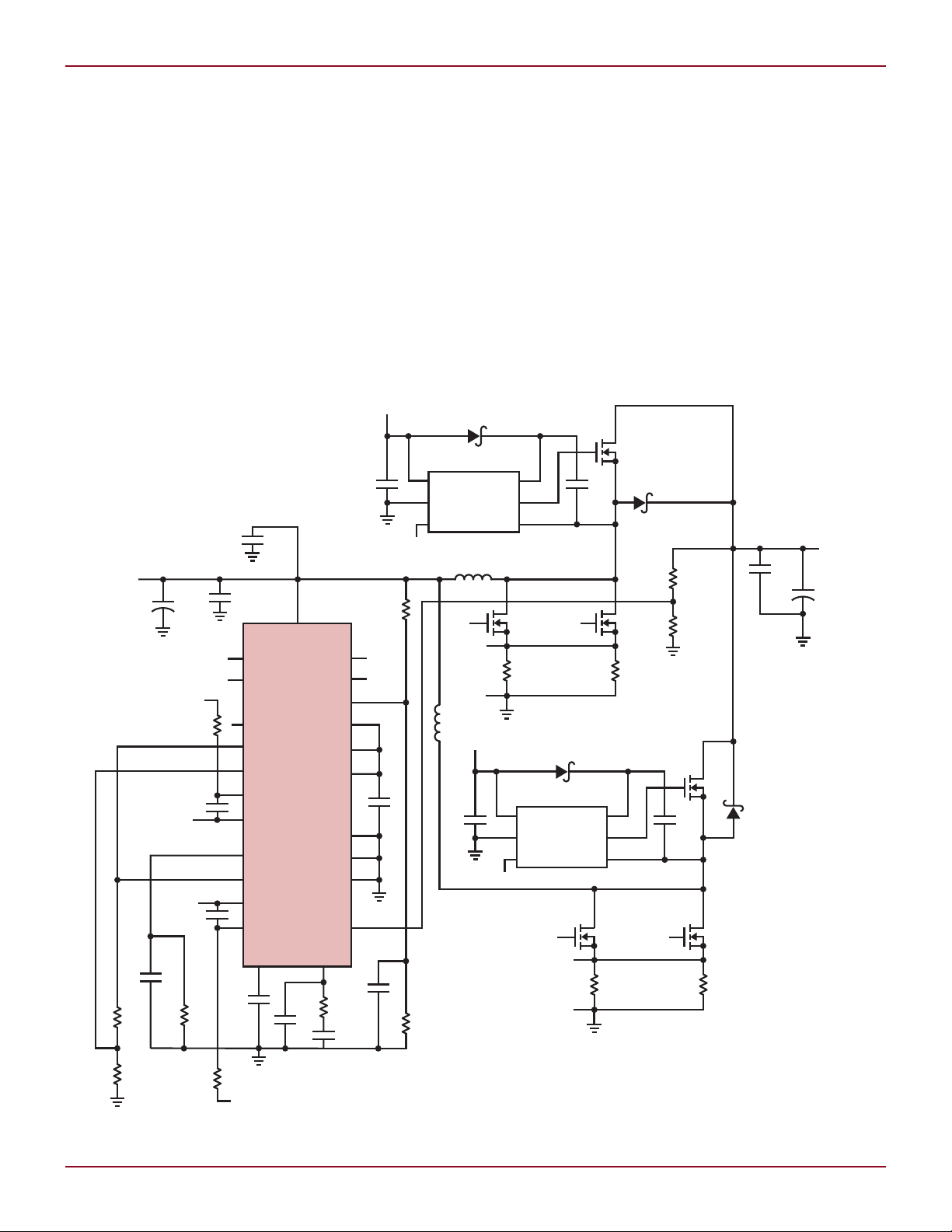
High Power 2-Phase Synchronous
Boost Replaces Hot Diodes with
Cool FETs—No Heat Sinks Required
by Narayan Raja, Tuan Nguyen and Theo Phillips
Introduction
For low power designs, non-synchronous boost converters offer a simple
solution. However, as power levels increase, the heat dissipated in the boost
diode becomes a significant design
problem. In such cases, a synchro-
nous boost converter, with the diode
replaced with a lower forward voltage
drop switch, significantly improves efficiency and relieves many issues with
thermal layout. Although the topology
is more complicated, Linear Technol-
ogy offers controller ICs that simplify
the design of high power synchronous
boost applications. The LT3782A boost
controller, for instance, includes predrive outputs for external synchronous
switch drivers. It also integrates strong
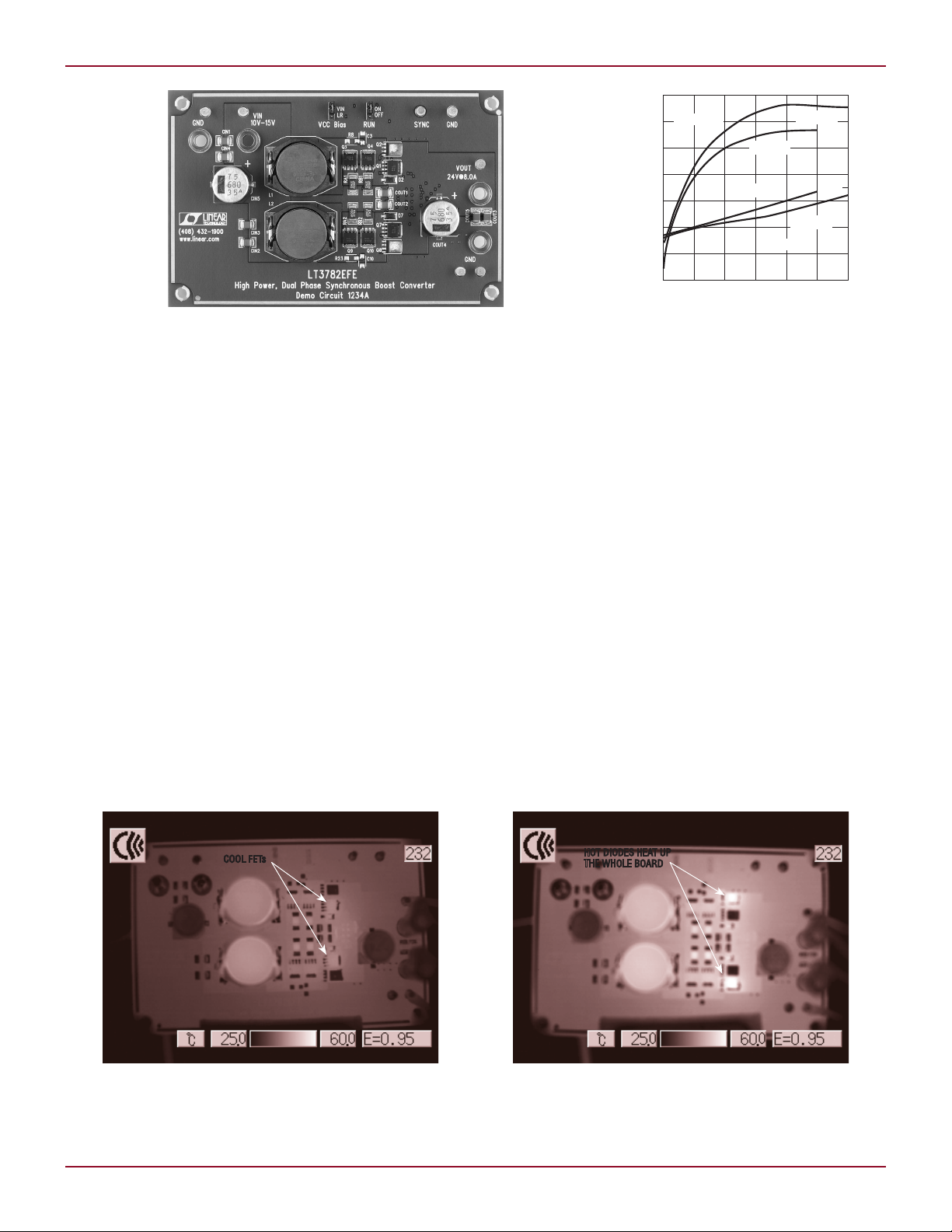
Figure 1. Compact high power boost application efficiently produces a 24V/8A output from a 10V–15V input.
Linear Technology Magazine • January 2009
3535
L DESIGN IDEAS
POWER LOSS (W)
EFFICIENCY (%)
LOAD CURRENT (A)
71
100
10
1
2
3 4
5 6
97
96
94
95
93
92
91
90
VIN = 12V
VIN = 12V
VIN = 24V
VIN = 24V
EFFICIENCY
POWER LOSS
Figure 2. Layout of the circuit in Figure 1. Note that no heat sinks are needed,
even at the high power levels produced by this relatively compact circuit.
bottom switch drivers for high gate
charge high voltage MOSFETs and
uses a constant frequency, peak current mode architecture to produce
high output voltages from 6V to 40V
inputs. Its 2-phase architecture keeps
external components small and low
profile.
Synchronous Operation
At high current levels, a boost diode
dissipates a significant amount of
power, while a synchronous switch
can burn far less. It all comes down
to the forward voltage drop. The power
dissipated in the boost diode is IIN • VD,
while the power dissipated by the
synchronous switch is I
(or I
IN
• V
). A typical sub-10mΩ
DS(ON)
MOSFET running 10A dissipates
1W, while the 0.5V drop of a typical
2
IN
• R
DS(ON)
.
Schottky diode burns a whopping
5W. Because the forward drop of a
synchronous MOSFET is proportional
to the current flowing through it, FETs
can be paralleled to share current and
drastically reduce power dissipation.
On the other hand, paralleling boost
diodes does little to reduce power dissipation as the forward drop through
the diodes holds fairly constant. The
non-synchronous boost diode topology
is more than just inefficient relative
to a synchronous solution—the extra
heat generated in a boost diode must
go somewhere, necessitating a larger
package footprint and heat sinking. At
high power levels, a non-synchronous
boost application becomes larger in
size and higher in cost over a synchronous solution.
Figure 3. Efficiency and power loss of the
circuit in Figure 1 compared to the efficiency
of the circuit when the synchronous FETs are
replaced with non-synchronous boost diodes.
Multiphase Operation
Reduces Application Size
There are a number of good reasons
to choose a multiphase/multi-channel
DC/DC converter over an equivalent
single-phase solution, including
reduced EMI and improved thermal
performance, but the biggest advantage can be a significant reduction in
application size. Although a 2-phase
solution requires more components,
two inductors and two MOSFETs instead of one, it offers a net reduction
in space and cost. This is because the
inductors and MOSFETs are more
than proportionally smaller than those
required in the single-phase solution.
Moreover, because the switching signals are mutually anti-phase, their
output ripples tend to cancel each
continued on page 39
COOL FETs
a. Thermal image of the board in Figure 2
built up with synchronous FETs
Figure 4. The board in Figure 2 runs fairly cool (a), but when the synchronous FETs are replaced with boost diodes, the entire board heats up
considerably with the diodes running significantly hotter than the FETs (b). (V
36
36
= 12V, I
IN
HOT DIODES HEAT UP
THE WHOLE BOARD
b. Thermal image of the board in Figure 2
built up with boost diodes
= 6A, two minutes after power up.)
LOAD
Linear Technology Magazine • January 2009

V
IN
LT3756
GND
SHDN/UVLO
INTV
CC
499k
110k
2.49k
130k
1M
140k
0.25Ω
10V–50V
2.2µF
50V
s2
V
IN
9V TO 36V
(6V UVLO)
L1
22µH
M1: VISHAY SILICONIX Si7454DP
D1: DIODES INC. PDS3100
L1: SUMIDA CDRH127-220
4.7k
LED
–
LED
+
0.1µF
4.7µF
CTRL
V
C
5.1k
10k
100k
4700pF
OPENLED
SS
FB
ISN
ISP
PWMOUT
PWM
V
REF
SENSE
R
T
GATE
C
OUT
2.2µF
100V
s2
M1
D1
28.7k
400kHz
0.025Ω
V
IN
3906
I
LED
400mA
EFFICIENCY (%)
VIN (V)
V
LED
= 10V
V
LED
= 50V
3010
100
0
15 20 25
10
20
30
40
50
60
70
80
90
Figure 4. A buck-boost mode LED driver with wide-ranging V
current; the peak inductor current
is also equal to the peak switching
current—higher than either a buck
mode or boost topology LED driver
with similar specs due to the nature
of the hookup. The 4A peak switch
current and inductor rating reflects
the worst-case 9V input to 50V LED
string at 400mA.
Below 9V input, the CTRL analog
dimming input pin is used to scale back
LT3782A, continued from page 36
other out, thus reducing the total
output ripple by 50%, which in turn
reduces output capacitance requirements. The input current ripple is also
halved, which reduces the required
input capacitance and reduces EMI.
Finally, the power dissipated as heat is
spread out over two phases, reducing
the size of heat sinks or eliminating
them altogether.
24V at 8A from
a 10V–15V Input
Figure 1 shows a high power boost
application that efficiently produces a
24V/8A output from a 10V–15V input.
The LTC4440 high side driver is used
Linear Technology Magazine • January 2009
and V
IN
LED
the LED current to keep the inductor
current under control if the battery
voltage drops too low. The LEDs turn
off below 6V input due to undervoltage
lockout and will not turn back on until
the input rises above 7V, to prevent
flickering. In buck-boost mode, the
output voltage is the sum of the input
voltage and the LED string voltage. The
output capacitor, the catch diode, and
small) strings of high power LEDs.
It can be used in boost, buck-boost
mode, buck mode, SEPIC and flyback
topologies. Its high voltage rating, optimized LED driver architecture, high
performance PWM dimming, host of
protection features and accurate high
side current sensing make the LT3756
a single-IC choice for a variety of high
voltage input and high power lighting
systems.
to level shift the SGATE signals and
drive the synchronous MOSFETs. The
250kHz switching frequency optimizes
efficiency and component size/board
area. Figure 2 shows the layout. Proper
routing and filtering of the sense pins,
placement of the power components
and isolation using ground and supply planes ensure an almost jitter free
operation, even at 50% duty cycle.
Figure 3 shows the efficiency of the
circuit in Figure 1 with synchronous
MOSFETs (measured to 8A) and the
efficiency of an equivalent non-synchronous circuit using boost diodes
(measured to 6A). The 1% improvement
in peak efficiency may not seem significant, but take a look at the difference
in heat dissipation shown in Figure 4,
which shows thermal images of both
circuits under equivalent operating
conditions. The thermal advantages
of using synchronous switches are
clear.
Conclusion
The 2-phase synchronous boost
topology possible with the LT3782A
offers several advantages over a nonsynchronous or a single-phase boost
topology. Its combination of high efficiency, small footprint, heat sink-free
thermal characteristics and low input/output capacitance requirements
make it an easy fit in automotive and
industrial applications.
DESIGN IDEAS L
Figure 5. Efficiency for the buck-boost
mode converter in Figure 4
the power MOSFET can see voltages
as high as 90V for this design.
Conclusion
The 100V LT3756 controller is ostensibly a high power LED driver, but its
architecture is so versatile, it can be
used in any number of high voltage
input applications. Of course, it has
all the features required for large (and
L
L
3939
 Loading...