

High Efficiency 2-Phase Boost Converter Minimizes Input and
Output Current Ripple –
Design Note 371
Goran Perica
Introduction
Many automotive and industrial applications require higher
voltages than is available on the input power supply rail.
A simple DC/DC boost converter suffices when the power
levels are in the 10W to 50W range, but if higher power
levels are required, the limitations of a straightforward
boost converter become quickly apparent. Boost converters convert a low input voltage to a higher output
voltage by processing the input current with a boost
inductor, power switch, output diode and output capacitor. As the output power level increases, the currents in
these components increase as well. Switching currents
INPUT
10V TO 23V
13.3k
4.7nF
80.6k
12.4k
75k
12k
1
RUN
2
I
TH
4
FREQ
5
MODE/SYNC
3
V
FB
LTC1871-7
229k
GATE
SENSE
INTV
GND
V
IN
CC
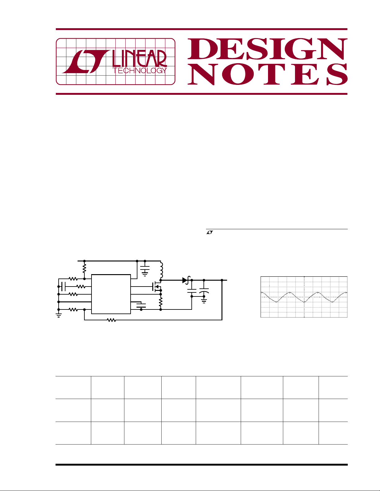
Figure 1a. Single-Phase Boost Converter: Can be Used
to Convert 12V Input to 24V, 10A Output
22μF
L1
×2
4.7μH
HAT2165
×2
0.002Ω
MBRB2545
22μF
×6
9
7
10
8
4.7μF
6
L1: COOPER HC3-4R7
ALL CERAMIC CAPACITORS ARE X7R, TDK
also increase proportional to the output-to-input voltage
conversion ratio, so if the input voltage is low, the
switching currents can overwhelm a simple boost converter and generate unacceptable EMI.
For example, consider Figure 1, a 12V input to 24V, 10A
output switching converter operating at 300kHz. The
currents processed by the converter in Figure 1 are shown
in the first row of Table 1. The relatively high current levels
in the switcher are reflected in high input and output ripple
currents, which results in increased EMI.
, LTC, LT and Burst Mode are registered trademarks of Linear Technology
Corporation. All other trademarks are the property of their respective owners.
OUTPUT
24V
+
220μF
10A
DN371 F01
V
OUT
100mV/DIV
1μs/DIV
DN371 F01b
Figure 1b. Single-Phase Boost
Converter Output Voltage Ripple
Table 1. Dual-Phase Boost Converter Has Lower Input and Output Ripple Currents and Voltages Than Single-Phase Boost
Converter
MOSFET OUTPUT OUTPUT OUTPUT OUTPUT
INPUT RMS INPUT RIPPLE RMS DRAIN DIODE CAPACITOR CAPACITOR VOLTAGE
CURRENT CURRENT CURRENT RMS CURRENT RMS CURRENT FREQUENCY RIPPLE
SINGLE-PHASE
BOOST 21.1A 4.2A
CONVERTER
DUAL-PHASE
BOOST 20.7A 0.17A
CONVERTER
09/05/371
P-P
P-P
15.4A 14.4A 10.5A 300kHz 212mV
2 × 7.4A 2 × 7.2A 1.9A 600kHz 65mV
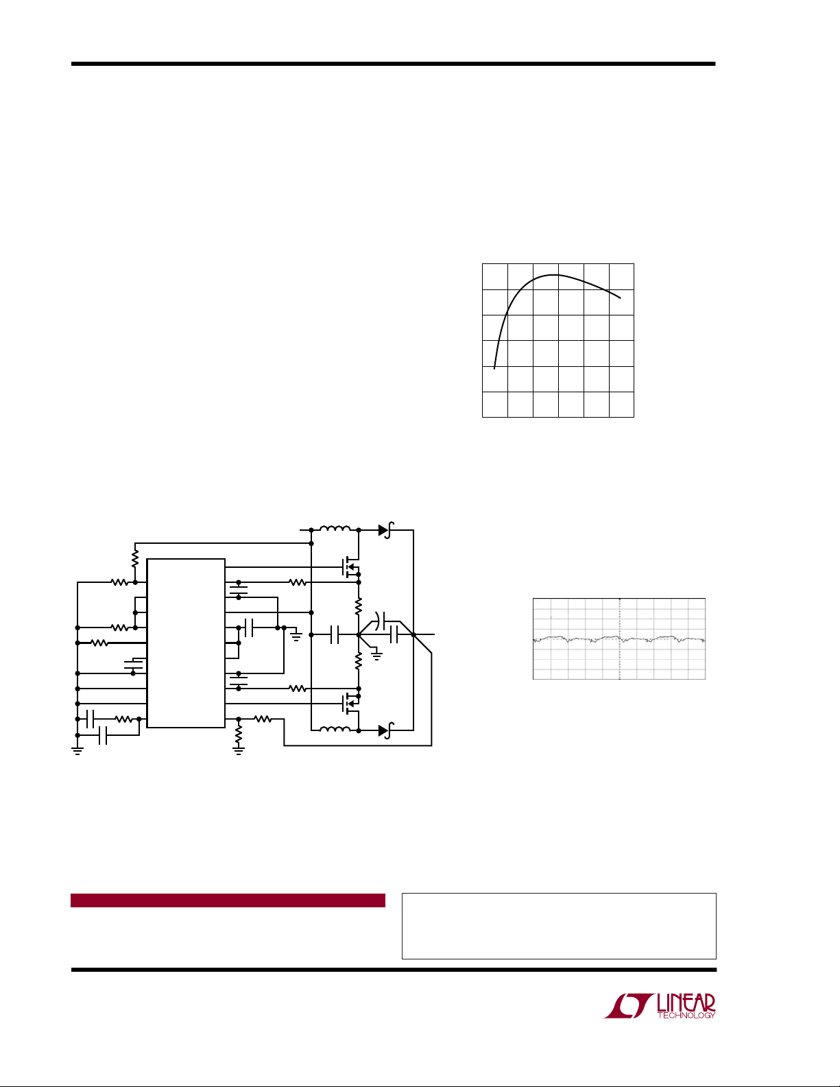
The circuit shown in Figure 2 performs the same DC/DC
conversion, but with greatly reduced input and output
ripple, significantly reducing EMI, and at a higher effective switching frequency, which allows the use of two
22μF output capacitors versus six 22μF output capacitors
required in Figure 1.
The trick is the 2-phase boost topology, which interleaves
two 180° out-of-phase output channels to mutually cancel out input and output ripple current—the results are
shown in the second row of Table 1. Each phase operates
at 50% duty cycle and the rectified output currents from
each phase flow directly to the load—namely the low
inductor ripple current—so only a small amount of output
current (shown in Table 1) is handled by the output
capacitors.
The centerpiece of the design in Figure 2 is the LT
®
3782
2-phase current mode PWM controller. Current mode
operation ensures balanced current sharing between the
two power converters resulting in even power dissipation
between the power stages.
The efficiency of the dual-phase converter, shown in
Figure 3, is high enough that it can be built entirely with
surface mount components—no need for heat sinks. In a
240W boost supply application, the power dissipation of
12.9W is relatively easy to manage in a well laid out, large
multilayer PCB with some forced airflow.
Conclusion
The simple LT3782 dual-phase switching boost converter
improves on single-phase alternatives by allowing high
power output with lower ripple currents, reduced heat
dissipation and a more compact design.
96
95
94
93
EFECIENCY (%)
92
91
90
0
468
2
OUTPUT CURRENT (A)
Figure 3. 12V Input to 24V Output Dual-Phase
Boost Converter Efficiency
10 12
DN371 F03
UPS840
HAT2165
220μF
HAT2165
UPS840
22μF
×2
+
59k
4.7nF
4.7nF
100pF
825k
274k
62k
15k
RUN
R
SET
DELAY
DCL
SLOPE
SS
GND
V
EE1
V
EE2
V
C
LT3782
BGATE1
SEN1P
SEN1N
V
GBIAS
GBIAS1
GBIAS2
SEN2N
SEN2P
BGATE2
INPUT
10V TO 23V
10nF
CC
FB
2.2μF
10nF
220k
24.9k
L1, L2: PULSE PB2020-153
ALL CERAMIC CAPACITORS ARE X7R TDK
L1
10Ω
0.004Ω
22μF
0.004Ω
10Ω
L2
Figure 2a. Dual-Phase Boost Converter Reduces EMI and Ripple
Currents with a Minimum Input and Output Filtering
Data Sheet Download
http://www.linear.com
OUTPUT
24V
10A
V
OUT
100mV/DIV
Figure 2b. Dual-Phase Boost
Converter Output Voltage Ripple
DN371 F02
For applications help,
call (408) 432-1900, Ext. 2593
1μs/DIV
DN371 F02b
Linear Technology Corporation
1630 McCarthy Blvd., Milpitas, CA 95035-7417
(408) 432-1900 ● FAX: (408) 434-0507 ● www.linear.com
dn371f LT/TP 0905 305K • PRINTED IN THE USA
© LINEAR TECHNOLOGY CORPORATION 2005
 Loading...