

Transistor Synchronous Forward Controller
FEATURES
■
High Voltage Operation up to 72V
■
Synchronizable Operating Frequency and Output
Switch Phase for Multiple Controller Systems
■
Synchronous Switch Output
■
Undervoltage Lockout Protection with 6V Hysteresis
for Self-Biased Power
■
Fixed Frequency Operation to 350kHz
■
Local ±1% Voltage Reference
■
Input Overvoltage Protection
■
Low Start-Up Current
■
Programmable Start Inhibit for Power Supply
Sequencing and Protection
■
Optocoupler Support
■
Soft-Start Control
U
APPLICATIO S
■
Isolated Telecommunication Systems
■
Personal Computers and Peripherals
■
Distributed Power Step-Down Converters
■
Lead Acid Battery Backup Systems
■
Automotive and Heavy Equipment
U
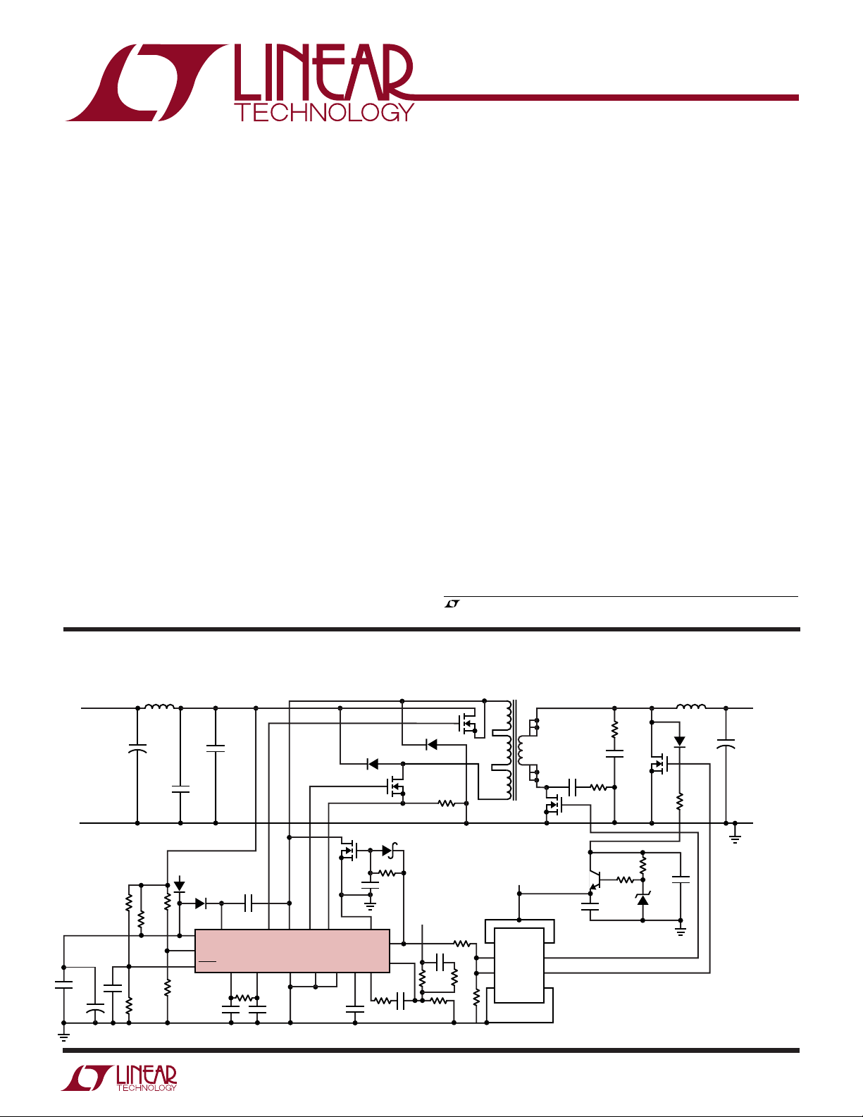
TYPICAL APPLICATIO
L1
+
V
IN
–
V
IN
4.7µH
C2
+
22µF
100V
C3
1.5µF
100V
C4
1.5µF
100V
Synchronous Forward Converter (Quarter-Brick Footprint)
36V-72V to 5V/7A DC/DC
MURS120T3
Q3
ZVN3310F
BAT54
LT3781
“Bootstrap” Start Dual
U
DESCRIPTIO
The LT®3781 controller simplifies the design of high
power synchronous dual transistor forward DC/DC converters. The part employs fixed frequency current mode
control and supports both isolated and nonisolated topologies. The IC drives external N-channel power MOSFETs
and operates with input voltages up to 72V.
The LT3781 is ideal for output derived power schemes,
through the use of a large undervoltage lockout hysteresis
range. The part is also equipped with an 18V VCC shunt
regulator, which prevents exceeding absolute maximum
ratings while in trickle start applications.
The LT3781’s operating frequency is programmable and
can be synchronized up to 350kHz. Switch phase is also
controlled during synchronized operation to accommodate multiple-converter systems. Internal logic guarantees 50% maximum duty cycle operation to prevent transformer saturation.
The LT3781 is available in a 20-lead SSOP package.
, LTC and LT are registered trademarks of Linear Technology Corporation.
L2
4.7µH
MBR0540T1
4.7Ω
+
C5
330µF
10V
MURS120T3
0.025Ω
1/2W
T1
•
Q1
R9
6
1
7
2
3
•
•
5
8
10
11
•
4
12
9
Q5
1nF
100V
0.25W
1nF
100V
10Ω
0.25W
10Ω
Q6
V
= 5V
OUT
= 7A
I
OUT
+
V
OUT
–
V
OUT
68µF
20V
0.1µF
1OV
BIAS
MMBD914LT1
73.2k
270k
0.25W
+
1nF
10k
20k
1%
BAS21
13
2
1
1.24k
1%
0.1µF
100V
20
V
V
CC
BST
OVLO
SHDN
FSET
5V
REF
5
52.3k
1µF 150pF
19
BSTREF
TG
LT3781
THERM
6
11
15
18
SENSE
BG
SYNC SGND
374
4.7nF
PGND
V
8SS10
14
V
C
100Ω
10k
330pF
SG
FB
12
9
0.01µF
OUT
5V
0.047µF
3.01k
1%
1k
1%
3.3k
51Ω
6.8k
8
V
3
IN2
1
IN1
4
GND2
1OV
BIAS
LTC1693-2
CC1
FZT690
4.7µF
16V
6
V
CC2
5
OUT2
7
OUT1
2
GND1
C2:SANYO 100MV22AX
C3, C4: VITRAMON VJ1825Y155MXB
C5: 4X KEMET T510X337KO10AS
L1: COILCRAFT DO1608C-472
100Ω
CMPZ5242B
12V
2k
0.22µF
50V
L2: PANASONIC ETQP6F4R1LF4
Q1,Q3:100V SILICONIX SUD40N10-25
Q5,Q6: SILICONIX Si4450
T1:COILTRONICS VP5-1200
3781f
1
LT3781
WW
W
U
ABSOLUTE AXI U RATI GS
(Note 1)
Power Supply (VCC)
Low Impedance Source Voltage ............. –0.3V to 20V
Shutdown Mode:
(Supply Self-Regulates to 18V)
Maximum Input Current ............................... 20mA
Topside Supply (V
V
BSTREF
– 0.3V to V
Topside Reference Pin (V
SHDN Pin Voltage........................... –0.3V to V
All Other Input Voltages.............. –0.3V to 5V
5V
Pin Sink Current ......................................... 10mA
REF
FSET Pin Current ...................................... –2mA to 5mA
All Other Input Pin Currents...................... –2mA to 2mA
Operating Ambient
Temperature Range (Note 4) ...............–40°C to 85°C
Operating Junction
Temperature Range ...............................–40°C to 125°C
Storage Temperature Range ..................–65°C to 150°C
Lead Temperature (Soldering, 10 sec).................. 300°C
) ....................................................
BST
BSTREF
BSTREF
+20V (V
BST(MAX)
) ...............–0.6V to 75V
= 90V)
CC
+ 0.3V
REF
+ 0.3V
UUW
PACKAGE/ORDER I FOR ATIO
TOP VIEW
1
SHDN
2
OVLO
3
THERM
4
SGND
5
5V
REF
6
FSET
7
SYNC
8
SS
9
V
FB
10
V
C
G PACKAGE
20-LEAD PLASTIC SSOP
T
= 125°C, θJA = 90°C/W
JMAX
Consult LTC Marketing for parts specified with wider operating temperature ranges.
20
19
18
17
16
15
14
13
12
11
V
BST
TG
BSTREF
NC
NC
BG
PWRGND
V
CC
SG
SENSE
ORDER PART
NUMBER
LT3781EG
LT3781IG
ELECTRICAL CHARACTERISTICS
The ● denotes specifications which apply over the full operating temperature range, otherwise specifications are TA = 25°C.
VCC = V
SYMBOL PARAMETER CONDITIONS MIN TYP MAX UNITS
Supply and Protection
V
CCUVLO
V
CCSHDN
I
CC
V
BST
V
SHDN
I
SS
V
SS
V
BSTUVLO
5V External Reference
V
5VREF
I
5VREFSC
R
5VREF
= 12V, V
BST
Undervoltage Lockout Threshold Falling Edge ● 8.0 8.4 8.6 V
Shutdown Mode Shunt Regulator 100µA < I
DC Active Supply Current (Note 2) 17 22 mA
DC Active UVLO Supply Current V
DC Standby Supply Current V
DC Active Supply Current TG Logic High (Note 2) ● 5.0 8.5 mA
DC Standby Supply Current V
Shutdown Rising Threshold ● 1.15 1.25 1.35 V
Shutdown Threshold Hysteresis 100 150 200 mV
Soft-Start Charge Current VSS = 2V ● –14 –10 –6 µA
Soft-Start Reset Threshold 225 mV
Boost Undervoltage Lockout Falling Edge ● 5.7 6.4 7.1 V
(V
-BSTREF) Rising Edge ● 6.5 7.0 7.5 V
BST
Boost UVLO Hysteresis ● 0.3 0.6 V
5V Reference Voltage 0 ≤ (I
Short-Circuit Current Source, IVC = 0 ● 20 45 mA
Output Impedance 0 ≤ (I
= 0V, VVC = 2V, VFB = V
BSTREF
= 1.25V, CTG = CBG = CSG = 1000pF.
REF
Rising Edge
≤ 10mA ● 16.5 18 19.9 V
VCC
= 1.35V, VCC = 8V ● 800 1200 µA
SHDN
< 0.3V ● 16 30 µA
SHDN
< 0.3V 0.1 µA
SHDN
– IVC) < 20mA 4.85 5.0 5.10 V
5VREF
– IVC) < 20mA 1 Ω
5VREF
● 13 14.5 16 V
● 25 mA
● 4.80 5.15 V
3781f
2

LT3781
ELECTRICAL CHARACTERISTICS
The ● denotes specifications which apply over the full operating temperature range, otherwise specifications are TA = 25°C.
VCC = V
SYMBOL PARAMETER CONDITIONS MIN TYP MAX UNITS
Error Amp
V
FB
I
FB
A
V
I
VC
V
VC
GBW Gain Bandwidth Product (Note 3) 1 MHz
Current Sense
A
V
I
SENSE
V
SENSE
t
D
t
MIN
THERM and OVLO Fault Detectors
V
THERM
V
OVLO
t
D
Oscillator and Synchronization Decoder
f
OSC
I
FSET
V
SYNC
f
SYNC
t
H, L
Output Drivers
V
TG
t
TGr/f
V
BG
t
BGr/f
V
SG
t
SGr/f
t
SG-BG
t
TG-BG
= 12V, V
BST
= 0V, VVC = 2V, VTS = 0V, VFB = V
BSTREF
= 1.25V, CTG = CBG = CSG = 1000pF.
REF
Error Amplifier Reference Voltage Measured at Feedback Pin 1.242 1.250 1.258 V
● 1.225 1.265 V
Feedback Input Current VFB = V
REF
–50 nA
Error Amplifier Voltage Gain 72 dB
Error Amplifier Current Limit Source ● 10 25 mA
Sink
● 0.5 1 mA
Zero Current Output Voltage 1.4 V
Maximum Output Voltage 3.2 V
Amplifier DC Gain 12 V/V
Input Bias Current –275 µA
Current Limit Threshold Measured at SENSE Pin 135 150 165 mV
● 130 170 mV
Current Sense to Switch Delay 175 ns
Switch Minimum On Time Measured at BG Output 250 ns
/ Threshold (Rising Edge) ● 1.2 1.25 1.3 V
Threshold Hysteresis ● 20 40 60 mV
Fault Delay to Output Disable >50mV Overdrive 650 ns
Oscillator Frequency, Free Run Measured at F
Frequency Programming Error f
FSET Input Bias Current F
≤ 500kHz (Note 3) ● –10 5 %
OSC
Charging, V
SET
Pin 700 kHz
SET
= 2V 50 nA
FSET
SYNC Logic High Input Threshold Positive-Going Edge ● 1.4 2 V
SYNC Logic Low Input Threshold Negative-Going Edge ● 0.8 1.4 V
SYNC Frequency ● f
Maximum SYNC Pulse Width f
= Oscillator Free-Run Frequency 1/f
OSC
/2 350 kHz
OSC
OSC
(Logic High or Logic Low)
TG On Voltage ● 11 11.5 V
TG Off Voltage
● 0.1 0.5 V
TG Rise/Fall Time 10% to 90%/90% to 10% 35 ns
BG On Voltage ● 11 11.5 12 V
BG Off Voltage
● 0.1 0.5 V
BG Rise/Fall Time 10% to 90%/ 90% to 10% 35 ns
SG On Voltage ● 11 11.5 12 V
SG Off Voltage
● 0.1 0.5 V
SG Rise/Fall Time 10% to 90%/ 90% to 10% 35 ns
SG to BG Enable Lag Time 4V On/Off Thresholds ● 80 150 300 ns
TG to BG Enable Lag Time 4V On/Off Thresholds 100 ns
s
3781f
3
LT3781
ELECTRICAL CHARACTERISTICS
Note 1: Absolute Maximum Ratings are those values beyond which the life
of a device may be impaired.
Note 2: Supply current specification does not include external FET gate
charge currents. Actual supply currents will be higher and vary with
operating frequency, operating voltages, and the type of external switch
elements used. See Applications Information.
Note 4: The LT3781E is guaranteed to meet performance specifications
from 0°C to 70°C. Specifications over the –40°C to 85°C operating
ambient temperature range are assured by design, characterization and
correlation with statistical process controls. For guaranteed performance
to specifications over the –40°C to 85°C operating ambient temperature
range, the LT3781I is available.
Note 3: Guaranteed but not tested.
UW
TYPICAL PERFOR A CE CHARACTERISTICS
Shutdown Mode: VCC vs I
18.4
TA = 25°C
18.2
(V)
18.0
CC
V
17.8
CC
18.20
18.15
(V)
18.10
CC
V
18.05
Shutdown Mode: VCC vs
Temperature (ICC = 1mA)
17.6
100µ
300µ
ICC Supply Current
vs Temperature
20
19
18
17
SUPPLY CURRENT (mA)
CC
I
16
15
–55
–40
0
TEMPERATURE (°C)
1m
ICC (A)
3m
3781 • G01a
10m
18.00
–55
–40
40
0
TEMPERATURE (°C)
80 125
3781 • G01b
ICC Supply Current
vs VCC Supply Voltage
18
VCC = 12V
40
12580
3781 G01
TA = 25°C
17
16
SUPPLY CURRENT (mA)
CC
I
15
9
12
10
SUPPLY VOLTAGE (V)
14
1816
3781 G03
4
3781f
UW
SOFT-START PIN VOLTAGE (mV)
0
SOFT-START OUTPUT CURRENT (µA)
20
40
60
1000 200 300 400
3781 G12
500
TA = 25°C
TYPICAL PERFOR A CE CHARACTERISTICS
I
Boost Supply Current
BST
vs Temperature
5.2
5.1
5.0
ICC Supply Current
vs SHDN Pin Voltage
60
TA = 25°C
40
LT3781
UVLO ICC Supply Current
vs Temperature
1
0.8
4.9
BOOST SUPPLY CURRENT (mA)
BST
I
4.8
–55
–40
5V
REF
5.10
5.05
5.00
VOLTAGE (V)
REF
5V
4.95
4.90
–55
–40
0
TEMPERATURE (°C)
Voltage vs Temperature
0
TEMPERATURE (°C)
20
SUPPLY CURRENT (µA)
CC
I
40
12580
3781 G04
0
0.2 0.4 0.6 0.8
0
5V
SHDN PIN VOLTAGE (V)
Short-Circuit Current Limit
REF
1.0
1.2
3781 G05
vs Temperature
60
50
40
SHORT-CIRCUIT CURRENT LIMIT (mA)
REF
5V
40
12580
3781 G07
30
–55
–40
0
40
TEMPERATURE (°C)
12580
3781 G08
SUPPLY CURRENT (mA)
CC
0.6
UVLO I
0.5
–55
–40
0
TEMPERATURE (°C)
Error Amp Reference
vs Temperature
1.260
1.255
1.250
1.245
ERROR AMP REFERENCE (V)
1.240
–55
–40
0
TEMPERATURE (°C)
40
40
12580
3781 G06
12580
3781 G09
VC Pin Short-Circuit Current Limit
vs Temperature
25
20
15
PIN SHORT-CIRCUIT CURRENT LIMIT (mA)
C
V
10
–55
–40
0
40
TEMPERATURE (°C)
12580
3781 G10
Soft-Start Output Current
vs Temperature
12
VSS = 2V
11
10
9
SOFT-START OUTPUT CURRENT (µA)
8
–55
–40
0
TEMPERATURE (°C)
40
12580
3781 G11
Soft-Start Output Current
vs Soft-Start Pin Voltage
3781f
5
LT3781
TEMPERATURE (°C)
–55
2
CURRENT SENSE AMP BANDWIDTH (MHz)
3
5
6
7
–15
25
45 125
3781 G14
4
–35 5
65
85
105
8
UW
TYPICAL PERFOR A CE CHARACTERISTICS
U
PI FU CTIO S
SHDN (Pin 1): Shutdown Pin. Pin voltages exceeding
positive going threshold of 1.25V enables the LT3781.
150mV of input hysteresis resists mode switching instability.
The SHDN pin can be controlled by either a logic level input
or with an analog signal. This shutdown feature is typically
used for input supply undervoltage protection. A resistor
divider from the converter input supply to the SHDN pin
monitors that supply for control of system power-up
sequencing, etc.
An 18V clamp on the VCC pin is enabled during shutdown
mode, preventing a trickle start circuit from pulling that pin
above maximum operational levels. All other internal
functions are disabled during shutdown.
OVLO (Pin 2): Overvoltage Shutdown Sense. Typically
connected to input supply through a resistor divider. If pin
voltage exceeds 1.25V, LT3781 switching function is
disabled to protect boosted circuitry from exceeding absolute maximum voltage. 40mV of input hysteresis resists
mode switching instability. Exceeding the OVLO threshold
also triggers soft-start reset, resulting in a graceful recovery from an input transient event.
6
Soft-Start Output Current
vs Soft-Start Pin Voltage
60
40
20
SOFT-START OUTPUT CURRENT (µA)
0
10234
SOFT-START PIN VOLTAGE (V)
UU
TA = 25°C
3781 G13
Current Sense Amplifier
Bandwidth vs Temperature
5
THERM (Pin 3): System Thermal Shutdown. Auxiliary
shutdown pin that is typically used for system thermal
protection. If pin voltage exceeds 1.25V, LT3781
switching function is disabled. 40mV of input hysteresis
resists mode switching instability. Exceeding the THERM
threshold also triggers soft-start reset, resulting in a
graceful recovery.
SGND (Pin 4): Signal Ground Reference. Careful board
layout techniques must be used to prevent corruption of
signal ground reference. High-current switching paths
must be oriented on the converter ground plane such that
currents to/from the switches do not affect the integrity of
the LT3781 signal ground reference.
5V
(Pin 5): 5V Local Reference. Allows connection of
REF
external loads up to 20mA DC. Typically bypassed with
1µF ceramic capacitor to SGND. Reference output is
current limit protected to a typical value of 45mA. If the
load on the 5V reference exceeds the current limit value,
LT3781 switching function is disabled and the soft-start
function is reset.
FSET (Pin 6): Oscillator Timing Pin. Connect a resistor
(R
) from the 5V
FSET
(C
) from this pin to ground.
FSET
pin to this pin and a capacitor
REF
3781f

LT3781
U
UU
PI FU CTIO S
The LT3781 oscillator operates by monitoring the voltage
on C
FSET pin reaches 2.5V, the oscillator rapidly discharges
the capacitor with an average current of about 0.8mA.
Once the voltage on the pin is reduced to 1.5V, the pin
becomes high-impedance and the charging cycle repeats.
The oscillator operates at twice the switching frequency of
the controller.
Oscillator frequency f
relation:
fC
OSC FSET
SYNC (Pin 7): Oscillator Synchronization Input Pin with
TTL-Level Compatible Input. The SYNC input signal (at the
desired synchronized operating frequency) controls both
the internal oscillator (running at twice the SYNC frequency) and the output switch phase. If synchronization
function is not desired, this pin may be floated or shorted
to ground.
The LT3781 internal oscillator drives a toggle flip-flop that
assures a ≤50% duty-cycle condition during oscillator
free-run. The oscillator, therefore, runs at twice the operating frequency of the controller. The SYNC input decoder
incorporates a frequency doubling circuit for oscillator
synchronization, resetting the internal oscillator on both
the rising and falling edges of the input signal.
The SYNC input decoder also differentiates transition
phase and forces the toggle flip-flop to phase-lock with the
SYNC input. A transition to logic high on the SYNC input
signal corresponds to the initiation of a new switching
cycle (primary switches turning on pending current control) and a transition to logic low forces a primary switch
off state. As such, the maximum operating duty cycle is
equal to the duty cycle of the SYNC signal. The SYNC input
can therefore be used to reduce the maximum duty cycle
of the controller by reducing the duty cycle of the SYNC
input.
as it is charged via R
FSET
OSC
≅+ ++
05 10
64
––
.• •
R
. When the voltage on the
FSET
can be approximated by the
FSET
3
810
R
2
FSET
–
1
–
1
SS (Pin 8): Soft-Start. Connect a capacitor (CSS) from this
pin to ground.
The output voltage of the LT3781 error amplifier corresponds to the peak current sense amplifier output detected before resetting the switch outputs. The soft-start
circuit forces the error amplifier output to a zero sense
current for start-up. A 10µA current is forced from this pin
onto an external capacitor. As the SS pin voltage ramps up,
so does the LT3781 internally sensed current limit. This
effectively forces the internal current limit to ramp from
zero, allowing overall converter current to slowly increase
until normal output regulation is achieved. This function
reduces output overshoot on converter start-up. The softstart functions incorporate a 1VBE “dead zone” such that
a zero-current condition is maintained on the VC pin until
the SS pin rises to 1VBE above ground.
The SS pin voltage is reset to start-up condition during
shutdown, undervoltage lockout, and overvoltage or
overcurrent events, yielding a graceful converter output
recovery from these events.
VFB (Pin 9): Error Amplifier Inverting Input. Typically
connected to a resistor divider from the output and compensation components to the VC pin.
The VFB pin is the converter output voltage feedback node.
Input bias current of ~50nA forces pin high in the event of
an open feedback path condition. The error amplifier is
internally referenced to 1.25V.
Values for the V
to VFB feedback resistor (RFB1) and
OUT
the VFB to ground resistor (RFB2) can be calculated to
program converter output voltage (V
) via the following
OUT
relation:
V
= 1.25 • (RFB1 + RFB2)/RFB2
OUT
VC (Pin 10): Error Amplifier Output. The LT3781 error
amplifier is a low impedance output inverting gain stage.
The amplifier has ample current source capability to allow
easy integration of isolation optocouplers that require bias
currents up to 10mA. External DC loading of the VC pin
reduces the external current sourcing capacity of the
5V
pin by the same amount as the load on the VC pin.
REF
3781f
7

LT3781
U
UU
PI FU CTIO S
The error amplifier is typically configured using a feedback
RC network to realize an integrator circuit. This circuit
creates the dominant pole for the converter regulation
feedback loop. Integrator characteristics are dominated
by the value of the capacitor connected from the VC pin to
the VFB pin and the feedback resistor connected to the V
pin. Specific integrator characteristics can be configured
to optimize transient response.
The error amplifier can also be configured as a
transimpedance amplifier for use in secondary-side controller applications. (See the Applications Information
section for configuration and compensation details)
SENSE (Pin 11): Current Sense Amplifier (CSA)
Noninverting Input. Current is monitored via a ground
referenced current sense resistor, typically in series with
the source of the bottom side switch FET. Internal current
limit circuitry provides for a maximum peak value of
150mV across the sense resistor during normal operation.
SG (Pin 12): Synchronous Switch Output Driver. This pin
can be connected directly to gate of synchronous switch
if small FETs are used (C
of a gate drive buffer is recommended for peak efficiencies.
< 5000pF), however, the use
GATE
FB
BG (Pin 15): Bottom Side Primary Switch/Forward Switch
Output Driver. This pin can be connected directly to
gate(s) of primary bottom side and forward switches if
small FETs are used (C
use of a gate drive buffer is recommended for peak
efficiencies.
The BG output is enabled at the start of each oscillator
cycle in phase with the TG pin but is timed to “lag” the TG
output during turn-on and “lead” the TG output during
turn-off. These delays force the concentration of transitional losses onto the bottom side primary switch.
An adaptive blanking circuit disables the current sense
function (via the SENSE pin) while the BG pin is below 5V.
BSTREF (Pin 18): V
nects to source of topside external power FET switch.
TG (Pin 19): Topside (Boosted) Primary Output Driver.
This pin can be connected directly to gate of primary
topside switch if small FETs are used (C
however, the use of a gate drive buffer is recommended for
peak efficiencies.
V
(Pin 20): Topside Primary Driver Bootstrapped Sup-
BST
ply. This “boosted” supply rail is referenced to the BSTREF
pin.
BST
total < 5000pF), however, the
GATE
Supply Reference. Typically con-
< 5000pF),
GATE
The SG pin output is synchronized and out-of-phase with
the BG output. The control timing of the SG output cause
it to “lead” the primary switch path during turn-on by
150nS.
VCC (Pin 13): IC Local Power Supply Input. Bypass with at
a capacitor at least 10 times greater than C5V
incorporates undervoltage lockout that disables switching
functions if VCC is below 8.4V. The LT3781 supports
operational VCC power supply voltages from 9V to 18V
(20V absolute maximum). An 18V clamp on the VCC pin is
enabled during shutdown mode, preventing a trickle start
circuit from pulling that pin above maximum operational
levels during IC shutdown.
PWRGND (Pin 14): Output Driver Ground Reference.
Connect through low impedance trace to VIN decoupling
capacitor.
. LT3781
REF
Supply voltage is maintained by a bootstrap capacitor tied
from the V
pin. The charge on the capacitor is refreshed each switch
cycle through a Schottky diode connected from the V
supply (cathode) to the V
capacitor (C
the total load capacitance on the TG pin. A capacitor in the
range of 0.1µF to 1.0µF is generally adequate for most
applications. The bootstrap diode must have a reverse
breakdown voltage greater than the converter VIN. The
LT3781 supports operational V
90V (absolute maximum) referenced to ground.
Undervoltage Lockout disables the topside switch until
V
– BSTREF > 7.0V for start-up protection of the
BST
topside switch.
pin to the boosted supply reference (BSTREF)
BST
pin (anode). The bootstrap
BST
) must be at least 100 times greater than
BOOST
supply voltages up to
BST
CC
3781f
8

BLOCK DIAGRA
BST
TG
V
20
BSTREF
19
BG
18
15
W
SG
12
PWRGND
14
LT3781
SS
8
225mV
10µA
–
Q
R
S
1681 BD
+
NOL
LOGIC
f = ×2
T
S
PHASE
Q
DETECT
SQ
–
REF
5V
R
–
+
BLANKING
+
×12
LIM
I
–
ERROR AMP
+
1.25V
UVLO
(<8V)
×4
–
1.25V
REFERENCE
GENERATOR
+
+
1.25V
–
6
FSET
7
SYNC
18V
9
10
C
V
11
SENSE
13
FB
CC
V
V
+
1
SHDN
–
1.25V
2
OVLO
4
SGND
3781f
3
THERM
5
REF
5V
9

LT3781
WUUU
APPLICATIO S I FOR ATIO
Overview
The LT3781 is a high voltage, high current synchronous
regulator controller, optimized for use with dual transistor
forward topologies. The IC uses a constant frequency,
current mode architecture, with internal logic that prevents operation over 50% duty cycle. A unique synchronization scheme allows the system clock to be synchronized
up to an operational frequency of 350kHz, along with
phase control for easy integration of multicontroller systems. A local precision 5V supply rail is available for
external support circuitry and can be loaded up to 20mA.
Internal fault detection circuitry disables switching when
a variety of system faults are detected such as: input
supply overvoltage or undervoltage faults, excessive system temperature, and local supply overcurrent conditions.
The LT3781 has a current-limit soft-start feature, which
gradually increases the current drive capability of a converter system to yield a smooth start-up with minimal
overshoot. The soft-start circuitry is also used for smooth
recoveries from system fault conditions.
External FET switches are employed for the switch elements, and hearty switch drivers allow implementation of
high current designs. An adaptive blanking scheme built
into the LT3781 allows for correct current-sense blanking
regardless of switch size. The LT3781 employs a voltage
output error amplifier, providing superior integrator linearity and allowing easy high bandwidth integration of
optocoupler feedback for fully isolated solutions.
Theory of Operation (See Block Diagram)
The LT3781 senses the output voltage of its associated
converter via the VFB pin. The difference between the
voltage on this pin and an internal 1.25V reference is
amplified to generate an error voltage on the VC pin, which
is used as a threshold for the current sense comparator.
The current sense comparator gets its information from
the SENSE pin, which monitors the voltage drop across an
external current sense resistor. When the detected switch
current increases to the level corresponding to the error
voltage on the VC pin, the switches are disabled until the
next switch cycle.
During normal operation, the LT3781 internal oscillator
runs at twice the switching frequency. The oscillator
output toggles a T flip-flop, generating a 50% duty cycle
pulse that is used internally as the system clock for the IC.
When the output of this flip-flop transitions high, the
primary switches are enabled. The primary side switches
stay enabled until the transformer primary current, sensed
via the SENSE pin connected to a ground-referenced
resistor in series with the bottom side switch FET, is
sufficient to trip the current sense comparator and, in turn,
reset the RS latch. When the RS latch resets, the primary
switches are disabled and the synchronous switch is
enabled. The adaptive blanking circuit senses the bottom
side gate voltage and prevents current sensing until the
FET is fully enabled, preventing false triggering due to a
turn-on transition glitch. If the current comparator threshold is not obtained when the flip-flop output transitions
low, the RS latch is bypassed and the primary switches are
disabled until the next flip-flop output transition, forcing a
maximum switch duty cycle less than 50%.
System Fault Detection-The General Fault Condition
(GFC)
The LT3781 contains circuitry for detecting internal and
system faults. Detection of a fault triggers a “general fault
condition”, or GFC. When a GFC is detected, the LT3781
disables switching and discharges the soft-start capacitor. When the GFC subsides, the LT3781 initiates a startup cycle via the soft-start circuitry to assure a graceful
recovery. Recovery from a GFC is gated by the soft-start
capacitor discharge. The capacitor must be discharged to
a threshold of 225mV before the GFC can be concluded. As
the zero output current threshold of the SS pin is typically
a transistor VBE, or 0.7V, latching the GFC until a 225mV
threshold is achieved assures a zero output current state
in the event of a short-duration fault. A GFC is also
triggered during system state change event, such as
entering shutdown mode, to prevent any mode transition
abnormalities.
10
3781f

WUUU
APPLICATIO S I FOR ATIO
LT3781
Events that trigger a GFC are:
a) Exceeding the current limit of the 5V
b) Detecting an undervoltage condition on V
c) Detecting an undervoltage condition on 5V
REF
pin
CC
REF
d) Pulling the SHDN pin below the shutdown threshold
e) Exceeding the 1.25V fault detector threshold on
either the OVLO or THERM pins
OVLO and THERM pins is used to directly trigger a GFC. If
either of these pins are not used, they can be disabled by
connecting the pin to ground. The intention of the OVLO
pin is to allow the monitoring of the input supply to protect
from an overvoltage condition though the use of a resistor
divider from the input supply. Monitoring of system temperature (THERM) is possible through use of a resistor
divider using a thermistor as a divider component. The
5V
pin can provide the precision supply required for
REF
these applications. When these fault detection circuits are
disabled during shutdown or VCC pin UVLO conditions, a
reduction in OVLO and THERM pin input impedance to
ground will occur. To prevent excessive pin input currents,
low impedance pull-up devices must not be used on these
pins.
Undervoltage Lockout
The LT3781 maintains a low current operational mode
when an undervoltage condition is detected on the V
CC
supply pin, or when VCC is below the undervoltage lockout
(UVLO) threshold. During a UVLO condition on the V
CC
pin, the LT3781 disables all internal functions with the
exception of the shutdown and UVLO circuitry. The external 5V
supply is also disabled during this condition.
REF
Disabling of all switching control circuity reduces the
LT3781 supply current to <1mA, making for efficient
integration of trickle charging in systems that employ
output feedback supply generation.
The function of the high side switch output (TG) is also
gated by UVLO circuitry monitoring the bootstrap supply
(V
– BSTREF). Switching of the TG pin is disabled until
BST
the voltage across the bootstrap supply is greater than
7.4V. This helps prevent the possibility of forcing the high
side switch into a linear operational region, potentially
causing excessive power dissipation due to inadequate
gate drive during start-up.
Error Amplifer Configurations
The converter output voltage information is fed back to the
LT3781 onto the VFB pin where it is transformed into an
output current control voltage by the error amplifier. The
error amplifier is generally configured as an integrator and
is used to create the dominant pole for the main converter
feedback loop. The LT3781 error amplifier is a true high
gain voltage amplifier. The amplifier noninverting input is
internally referenced to 1.25V; the inverting input is the
VFB pin and the output is the VC pin. Because both low
frequency gain and integrator frequency characteristics
can be controlled with external components, this amplifier
allows far greater flexibility and precision compared with
use of a transconductance error amplifier.
In a nonisolated converter configuration where a resistor
divider is used to program the desired output voltage, the
error amplifier can be configured as a simple active
integrator, forming the system dominant pole ( Figure␣ 1).
Placing a capacitor C
set the single-pole crossover frequency at (2πRFBC
from the VFB pin to the VC pin will
ERR
ERR
)-1.
Additional poles and zeros can be added by increasing the
complexity of the RC network.
V
OUT
R
FB
Figure 1. Nonisolated Error Amp Configuration
V
FB
9
C
ERR
V
C
10
LT3781
–
+
1.25V
3781 F01
3781f
11

LT3781
WUUU
APPLICATIO S I FOR ATIO
Another common error amplifier configuration is for
optocoupler use in fully isolated converters with secondary side control (Figure 2). In such a system, the dominant
pole for the feedback loop is created at the secondary side
controller, so the error amplifier needs only to translate the
optocoupler information. The bandwidths of the
optocoupler and amplifier should be as high as possible to
simplify system compensation. This high bandwidth
operation is accomplished by using the error amplifier as
a transimpedance amplifier, with the optocoupler transistor emitter providing feedback information directly into
the VFB pin. A resistor from VFB to ground provides the DC
bias condition for the optocoupler. Connecting the
optocoupler transistor collector to the local 5V
reduces Miller capacitance effects and maximizes the
bandwidth of the optocoupler. Also, higher optocoupler
current means higher bandwidth, and the 5V
can provide collector currents up to 10mA.
V
OUT
SENSE
5
9
10
5V
REF
V
FB
V
C
LT3781
5V
–
+
1.25V
3781 F02
REF
REF
supply
supply
internally as the system clock for the IC. Free-run
frequency for the internal oscillator is programmed via an
RC timing network connected to the FSET pin. A pull-up
resistor R
provides current to charge a timing capacitor C
, connected from the 5V
FSET
pin to FSET,
REF
FSET
connected from the FSETpin to ground. The oscillator operates by allowing R
point R
is pulled back toward ground by a 2.5K resistor
FSET
internal to the LT3781. When the voltage across C
to charge C
FSET
up to 2.5V at which
FSET
FSET
is
pulled down to 1.5V, the FSET pin becomes high impedance, once again allowing R
Figure 3 is a plot of oscillator frequency vs C
to charge C
FSET
FSET
FSET
.
and R
FSET
is shown below. Typical values for 300kHz operation
(150kHz system frequency) are C
R
= 51kΩ.
FSET
600
550
500
450
400
350
300
250
200
OSCILLATOR FREQUENCY (kHz)
150
100
Figure 3. Oscillator Frequency vs. Timing Components
20
30 50
330pF
100pF
150pF
200pF
40
TIMING RESISTOR (kΩ)
60
= 150pF and
FSET
90
80
70
100
3781 F03
Figure 2. Optocoupler High-BW Configuration
Oscillator Frequency Programming and
Synchronization
The LT3781 internal oscillator runs at twice the system
switching frequency. The oscillator output toggles a T
flip-flop, generating a 50% duty cycle pulse that is used
12
Due the relatively fast fall time of the oscillator waveform,
the FSET pin is held at its 1.5V threshold by an internal low
impedance clamp to reduce undershoot error. As a result,
if this pin is externally forced low for any reason, external
current limiting is required to prevent damage to the
LT3781. Continuous source current from the FSET pin
should not exceed 1mA. Putting a 2k resistor in series with
any low impedance pull-down device will assure proper
function and protect the IC from damage.
3781f

WUUU
5V
REF
FSET
75k
51k 100pF
3781 F05
LT3781
5
6
APPLICATIO S I FOR ATIO
Oscillator Synchronization
Synchronization of the LT3781 system clock is accomplished by driving a TTL level logic pulse train at the
desired system switching frequency into the SYNC pin. In
order to assure proper synchronization, each phase of the
synchronization signal must be less than an oscillator
free-run cycle.
The SYNC input pulse controls the phasing as well as the
frequency of controller switching. The SYNC circuit functions by forcing the phase of the oscillator output flip-flop
to match the phase of the SYNC pulse and prematurely
ending the oscillator charge cycle on each transition edge.
At the SYNC logic low-to-high transition, the LT3781
starts a switch-on cycle and the minimum switch-off
period is forced during the SYNC logic low period. Because the SYNC logic low period corresponds directly to
the minimum off time, the converter maximum duty cycle
can be forced using the SYNC input. For example, a 30%
duty cycle SYNC pulse forces 30% maximum duty cycle
operation for the converter. Because the logic-low pulse
width exceeds the logic-high pulse width in < 50% duty
cycle operation, the oscillator free-run cycle time must be
programmed to exceed the logic-low duration.
LT3781
Figure 5. Oscillator Connection for SYNC-Only Mode Operation
Bootstrap Start
It is inefficient as well as impractical to power a controller
IC from a high-voltage input supply. Using a linear
preregulation scheme to provide the required VCC voltage
for the LT3781 would waste significant power, reducing
converter efficiencies and creating additional thermal concerns. Self-biased power schemes take advantage of
inherent converter efficiencies to significantly reduce losses
associated with powering the controller. Bootstrapped
power can be derived using auxiliary windings on the
power transformer or inductor, rectified taps on switching
nodes, or the converter output directly.
2.5V
FSET
1.5V
SYNC
SYSTEM
CLOCK
(INTERNAL)
Figure 4. Oscillator/SYNC Waveforms
3781 F04
It is also possible to run the LT3781 in a SYNC-only mode
by disabling the oscillator completely. Connecting a resistor divider from the 5V
pin to the FSET pin forcing a
REF
voltage within the charge range of 1.5V-2.5V will allow the
oscillator to follow the SYNC input exclusively with no
provision for free-run. Setting values to force a voltage as
close to 2V as possible is recommended.
Start-up circuitry built into the LT3781 allows VCC to
increase from 0V to 14.5V before the converter is enabled.
During this time, start-up current is less than 1mA. The
trickle current required for charging the VCC supply is
typically generated with a resistor from the converter high
voltage input. When combined with the VCC bypass capacitor, the current through the start-up resistor creates a
voltage ramp on VCC whose slope governs the turn-on
time of the converter. The low quiescent current of the
LT3781 allows the input voltage to be trickled up with
minimal power dissipation in the start-up resistor. At
VCC = 14.5V, the LT3781 internal circuitry is enabled and
switching begins. If enough bootstrap power is fed back
into VCC to keep that supply voltage above 8.4V, then
switching continues and a bootstrap start is accomplished. If the input voltage drops below 8.4V, the LT3781
is disabled and the switching regulator returns to the
start-up low current state.
3781f
13

LT3781
WUUU
APPLICATIO S I FOR ATIO
Shutdown
The LT3781 SHDN pin will support TTL and CMOS logic
signals and also analog inputs. The SHDN pin turn-on
(rising) threshold is 1.25V with 150mV of hysteresis. A
common use of the SHDN pin is for under voltage detection on the input supply. Driving the SHDN pin with a
resistor-divider connected from the input supply to ground
will prevent switching until the desired input supply voltage is achieved.
An 18V clamp on the VCC pin is enabled during shutdown
mode, preventing a trickle start circuit from pulling that pin
above maximum operational levels.
The LT3781 enters an ultralow current shutdown mode
when the SHDN pin is below 350mV. During this mode,
total supply current drops to a typical value of 16µA. When
SHDN rises above 350mV, the IC will draw increasing
amounts of supply current until just before the 1.25V
turn-on threshold is achieved, when the supply current
reaches 75µA.
The shutdown function can be disabled by connecting the
SHDN pin to VCC. This pin is internally clamped to 2.5V
through a 20k series input resistance and can therefore
draw almost 1mA when tied directly to the VCC supply. This
additional current can be minimized by making the connection through an external series resistor (100k is typically used).
Soft-Start
The SS pin sources a typical current of 10µA. Placing a
capacitor (CSS) from the SS pin to ground will cause the
voltage on the SS pin to ramp up at a controlled rate,
allowing a graceful increase of maximum converter output
current during a start-up condition. The start-up delay
time to full available current limit is:
tSS = 2.5 • 105 • CSS (sec)
The LT3781 internally pulls the SS pin below the zero
current threshold during any fault condition to assure
graceful recovery. The SS circuit also acts as a fault control
latch to assure a full-range recovery from a short duration
fault. Once a fault condition is detected, the LT3781 will
suspend switching until the SS pin has discharged to
approximately 225mV.
Layout Considerations-Grounding
The LT3781 is typically used in high current converter
designs that involve substantial switching transients. The
switch drivers on the IC are designed to drive large
capacitances and, as such, generate significant transient
currents. Careful consideration must be made regarding
input and local power supply bypassing to avoid corrupting the ground references used by the error amplifier and
current sense circuitry.
Effective grounding of the two-transistor synchronous
forward topology where the LT3781 is used is inherently
difficult. The situation is complicated further by the number of bypass elements that must be considered.
The LT3781 current control pin (VC) limits sensed current
to zero at voltage less than 1.4V through full current limit
at VC = 3.2V, yielding 1.8V over the full regulation range.
The voltage on the VC pin is internally forced to be less than
or equal to SS + 0.7V. As such, the SS pin has a “dead
zone” between 0V and 0.7V, where a zero sensed current
condition is maintained. At SS voltages above 0.7V, the
sensed current limit threshold on the VC pin may rise as
needed up to the SS maintained current limit value. Once
the SS pin rises to the VC pin maximum value less 0.7V, or
2.5V, the SS circuit has no effect.
14
Typically, high current paths and transients from the input
supply and any local drive supplies must be kept isolated
from SGND, to which sensitive circuits such as the error
amp reference and the current sense circuits, as well as the
local 5V
used in LT3781 applications, the large currents from the
primary switches, as well as the switch drive transients,
pass through the sense resistor to ground. This defines
the ground connection of the sense resistor as the reference point for both SGND and PGND. In nonisolated
applications where SGND is the output reference, we now
have a condition where every bypass capacitor in the
converter is referenced to the same point.
supply, are referred. By virtue of the topologies
REF
3781f

WUUU
APPLICATIO S I FOR ATIO
LT3781
Effective grounding can be achieved by considering the
return current paths from the sense resistor to each
respective bypass capacitor. Don’t be tempted to run
small traces to separate the grounds. A power ground
plane is important as always in high power converters, but
bypass elements must be oriented such that transient
LT3781
5V
REF
SGND
V
BST
BSTREF
V
CC
PGND
currents in the return paths of VIN and VCC do not mix. Care
must be taken to keep these transients away from the
SGND reference. An effective approach is to use a 2-layer
ground plane, reserving an entire layer for SGND. The
5V
and nonisolated converter output bypasses can
REF
then be directly connected to the SGND plane.
V
BST
V
CC
V
IN
Figure 6. High-Current Transient Return Paths
3781f
15

LT3781
V
CC
13
2
1
5
1µF 82pF
OVLO
SHDN
1.24k
1%
73.2k
1%
20k
10k
267k
0.25W
68µF
20V
5V
REF
6
F
SET
4700pF
8
SS
10
14
BAS21
BAT54
T2
S
S
BAS21
BAT54
BAT54
ZVN3310F
9
V
C
PGND
V
FB
374
THERM
LT3781
SYNC SGND
52.3k
10Ω
1k
3k
1k
3.3k
100Ω
0.25W
10k
2k
FZT690B
4.7µF
0.22µF
S
MMBZ5240BLT1
10V
1
3.3Ω
10k
5V
REF
ISO1
MOC207
7
143
3
1
4
6
5
14
15
6
5
82
3300pF
4700pF
0.1µF
5V
REF
12
SG
+
0.1µF
1nF
11
SENSE
15
BG
18
BSTREF
19
TG
20
BAS21
0.1µF
L3 1mH
V
BST
220pF
C4
1.5µF
100V
C3
1.5µF
100V
L1
4.7µH
0.022µF
1000pF
••
SYNC V
FB
OVPIN
MARGIN
I
COMP
V
DD
OPTODRV
V
AUX
0.1µF
12
I
SNS
11
I
SNSGND
16
FG
2
CG
PGND GND
LTC1698
PWRGD
6
8
9
7
13
1.24k
1%
976Ω
4.22k
1%
1043
V
COMP
3781 F07
3.01k
1k
0.1µF
MBR0530
0.030Ω
1/2W
1
2
5
4
Q3
NC
1000pF
100V
2.2nF
250V
1nF
100V
Q5, Q6
FDS6680A
×2
Q14, Q15
FDS6680A
×2
MURS120T3
MURS120T3
10Ω
6
11
10
879
12
•
•••
3
Q1
T1
10Ω
MMBT3906LT1
MMBT3906LT1
V
IN
+
V
IN
–
C2
1.5µF
100V
V
OUT
+
V
OUT
–
S
C5 TO C8
330µF
10V
×4
10Ω
0.25W
10Ω
0.25W
L2
4.8µH
330pF
+
C1: MURATA ERIE GHM3045X7R222K-GC
C2, C3, C4: VITRAMON VJ1825Y155MXB
C5 TO C8: 330µF 10V KEMET T510X337K010AS
OR 330µF 6.3V KEMET T520D337M006AS
ISO1: FAIRCHILD MOC207
L1: COILCRAFT DO1608C-472
L2: PANASONIC ETQPAF4R8HFA
L3: COILCRAFT DO1608C-105
Q1, Q3: SILICONIX Si4486EY
Q5, Q6, Q14,Q15: FAIRCHILD FDS6680A
T1: MIDCOM 31267R OR COILTRONICS CTX02-14675
(FUNCTIONAL INSULATION) OR
MIDCOM 31322R (BASIC INSULATION)
T2: MIDCOM 31264R
(FUNCTIONAL INSULATION) OR
MIDCOM 31323R (BASIC INSULATION)
4.7Ω
TYPICAL APPLICATIO S
U
Figure 7. 36V to 72V DC in to 5V/10A Isolated Synchronous Forward Converter
16
3781f

V
CC
13
2
1
5
1µF 82pF
OVLO
SHDN
1.24k
1%
73.2k
1%
20k
10k
267k
0.25W
C26
68µF
20V
5V
REF
6
F
SET
4700pF
8
SS
10
14
BAS21
BAT54
T2
S
S
BAS21
BAT54
BAT54
Q12
ZVN3310F
9
V
C
PGND
V
FB
374
THERM
LT3781
SYNC SGND
52.3k
1%
10Ω
1k
3k
1k
1k
100Ω
10k
2k
0.25W
Q13
FZT690B
4.7µF
16V
0.22µF
50V
S
MMBZ5240BLT1
10V
1
3.3Ω
10k
5V
REF
ISO1
MOC207
7
143
3
1
4
6
5
14
15
6
5
82
3300pF
4700pF
0.1µF
5V
REF
12
SG
+
0.1µF
1nF
11
SENSE
15
BG
18
BSTREF
19
TG
20
BAS21
0.1µF 100V
L3 1mH
V
BST
220pF
C4
1.5µF
100V
C3
1.5µF
100V
L1
3.3µH
0.022µF
1000pF
••
SYNC V
FB
OVPIN
MARGIN
I
COMP
V
DD
OPTODRV
V
AUX
0.1µF
12
I
SNS
11
I
SNSGND
16
FG
2
CG
PGND GND
LTC1698
PWRGD
6
8
9
7
TRIM
13
1.24k
1%
1.78k
1%
2.43k
1%
1043
V
COMP
1698 F11
3.01k
1k
0.33µF
MBR0530
0.025Ω
1/2W
3
4
Q3
1000pF
100V
C1
2200pF
250V
1000pF
100V
Q5, Q14
FDS6680A
×2
Q6, Q15, Q17
FDS6680A
×3
MURS120T3
MURS120T3
10Ω
2
7
V
SEC
5
•
••
1
Q1
T1
10Ω
MMBT3906LT1
MMBT3906LT1
V
IN
+
V
IN
–
C2
1.5µF
100V
V
OUT
+
V
OUT
–
S
C5 TO C8
330µF
10V
×4
10Ω
0.25W
10Ω
0.25W
4.7Ω
L2
2.35µH
330pF
+
C1: MURATA ERIE GHM3045X7R222K-GC
C2, C3, C4: VITRAMON VJ1825Y155MXB
C5 TO C8: 330µF 10V KEMET T510X337K010AS
OR 330µF 6.3V KEMET T520D337M006AS
C26: AVX TPSE686M020R0150
ISO1: FAIRCHILD MOC207
L1: COILCRAFT DO1608C-332
L2: PULSE P1977 PLANAR INDUCTOR
L3: COILCRAFT DO1608C-105
Q1, Q3: SILICONIX Si4486EY
Q5, Q6, Q14,Q15,Q17: FAIRCHILD FDS6680A
Q7: FAIRCHILD NDT410EL
Q12: ZETEX ZVN3310F
Q13: ZETEX FZT690
T1: PULSE P1976 PLANAR TRANSFORMER
(FUNCTIONAL INSULATION) OR
PULSE PA-0191 (BASIC INSULATION)
T2: MIDCOM 31264R (FUNCTIONAL INSULATION) OR
MIDCOM 31323R (BASIC INSULATION)
TYPICAL APPLICATIO S
LT3781
U
Figure 8. 36V to 72V DC in to 3.3V/20A Isolated Synchronous Forward Converter
3781f
17

LT3781
V
CC
13
2
1
5
1µF 82pF
OVLO
SHDN
1.24k
1%
73.2k
1%
20k
10k
267k
0.25W
C26
68µF
20V
5V
REF
6
F
SET
4700pF
8
SS
10
14
BAS21
BAT54
T2
S
S
BAS21
BAT54
BAT54
Q12
ZVN3310F
9
V
C
PGND
V
FB
374
THERM
LT3781
SYNC SGND
52.3k
1%
10Ω
1k
3k
1k
1k
100Ω
9V
10k
2k
0.25W
Q13
FZT690B
4.7µF
16V
0.22µF
50V
S
MMBZ5240BLT1
10V
1
3.3Ω
10k
5V
REF
ISO1
MOC207
7
143
3
1
4
6
5
14
15
6
5
82
3300pF
4700pF
0.1µF
5V
REF
12
SG
+
0.1µF
1nF
11
SENSE
15
BG
18
BSTREF
19
TG
20
BAS21
0.1µF 100V
L3 1mH
BLKSENS
V
BST
220pF
C4
1.5µF
100V
C3
1.5µF
100V
L1
3.3µH
0.022µF
1000pF
••
SYNC V
FB
OVPIN
MARGIN
I
COMP
V
DD
OPTODRV
V
AUX
0.1µF
12
I
SNS
11
I
SNSGND
16
FG
2
CG
PGND GND
LTC1698
PWRGD
6
8
9
7
13
1.24k
1%
1.78k
1%
3.01k
1%
SENSE
+
SENSE
–
TRIM
100Ω
0.25W
5
6
4
2
3
1
7
9V
V
OUT
+
2.43k
1%
1043
V
COMP
1698 F12
3.01k
1%
3.01k
1%
3.01k
1%
3.01k
1%
100Ω
0.25W
1k
0.33µF
MBR0530
0.025Ω
1/2W
3
4
Q3
1000pF
100V
C1
2200pF
250V
1000pF
100V
Q5, Q14
FDS6680A
×2
Q6, Q15, Q17
FDS6680A
×3
MURS120T3
MURS120T3
10Ω
2
7
V
SEC
5
•
••
1
Q1
T1
10Ω
MMBT3906LT1
MMBT3906LT1
V
IN
+
V
IN
–
C2
1.5µF
100V
V
OUT
+
V
OUT
–
S
C5 TO C8
330µF
10V
×4
10Ω
0.25W
10Ω
0.25W
4.7Ω
L2
2.35µH
330pF
+
62k
0.25W
MMBZ5248LT1
18V
MMBT3904LT1
47k
4.7µF
5V
REF
MMBD914LT1
Q7
NDT410EL
1.5k
0.25W
1.5k
0.25W
–
+
LT1006S8
C1: MURATA ERIE GHM3045X7R222K-GC
C2, C3, C4: VITRAMON VJ1825Y155MXB
C5 TO C8: 330µF 10V KEMET T510X337K010AS
OR 330µF 6.3V KEMET T520D337M006AS
C26: AVX TPSE686M020R0150
ISO1: FAIRCHILD MOC207
L1: COILCRAFT DO1608C-332
L2: PULSE P1977 PLANAR INDUCTOR
L3: COILCRAFT DO1608C-105
Q1, Q3: SILICONIX Si4486EY
Q5, Q6, Q14,Q15,Q17: FAIRCHILD FDS6680A
Q7: FAIRCHILD NDT410EL
Q12: ZETEX ZVN3310F
Q13: ZETEX FZT690
T1: PULSE P1976 PLANAR TRANSFORMER
(FUNCTIONAL INSULATION) OR
PULSE PA-0191 (BASIC INSULATION)
T2: MIDCOM 31264R (FUNCTIONAL INSULATION) OR
MIDCOM 31323R (BASIC INSULATION)
TYPICAL APPLICATIO S
U
Figure 9. 36V to 72V DC in to 3.3V/20A Isolated Synchronous Forward Converter with Fast Start and Differential Sense
18
3781f

PACKAGE DESCRIPTION
U
G Package
20-Lead Plastic SSOP (5.3mm)
(Reference LTC DWG # 05-08-1640)
1.25 ±0.12
LT3781
6.90 – 7.50*
(.272 – .295 )
1718 14 13 12 1115161920
7.8 – 8.2
0.42 ±0.03 0.65 BSC
RECOMMENDED SOLDER PAD LAYOUT
5.00 – 5.60**
(.197 – .221)
0.09 – 0.25
(.0035 – .010)
NOTE:
1. CONTROLLING DIMENSION: MILLIMETERS
2. DIMENSIONS ARE IN
3. DRAWING NOT TO SCALE
*
DIMENSIONS DO NOT INCLUDE MOLD FLASH. MOLD FLASH
SHALL NOT EXCEED .152mm (.006") PER SIDE
**
DIMENSIONS DO NOT INCLUDE INTERLEAD FLASH. INTERLEAD
FLASH SHALL NOT EXCEED .254mm (.010") PER SIDE
0.55 – 0.95
(.022 – .037)
MILLIMETERS
(INCHES)
5.3 – 5.7
0
° – 8°
12345678910
0.65
(.0256)
BSC
0.22 – 0.38
(.009 – .015)
7.40 – 8.20
(.291 – .323)
2.0
(.079)
0.05
(.002)
G20 SSOP 0802
Information furnished by Linear Technology Corporation is believed to be accurate and reliable.
However, no responsibility is assumed for its use. Linear Technology Corporation makes no representation that the interconnection of its circuits as described herein will not infringe on existing patent rights.
3781f
19

LT3781
RELATED PARTS
PART NUMBER DESCRIPTION COMMENTS
LT1158 Half-Bridge N-Channel MOSFET Driver Current Limit Protection, 100% of Duty Cycle
LT1160 Half-Bridge N-Channel MOSFET Driver Up to 60V Input Supply, No Shoot-Through
LT1162 Dual Half-Bridge N-Channel MOSFET Driver VIN to 60V, Good for Full-Bridge Applications
LT1336 Half-Bridge N-Channel MOSFET Driver Smooth Operation at High Duty Cycle (95% to 100%)
LT1339 High Power Synchronous DC/DC Controller 60V Dual N-Channel MOSFET Controller
LTC®1530 High Power Step-Down Switching Regulator Controller Excellent for 5V to 3.x Up to 50A
LTC1625 No R
LT1640 Negative Voltage Hot SwapTM Controller Allows Safe Board Insertion and Removal from a Live –48V Backplane,
LT1680 High Power DC/DC Current Mode Step-Up Controller High Side Current Sense, Up to 60V Input
LT1681 Dual Transistor Synchronous Foward Controller Operation up to 72V Maximum
LTC1696 Overvoltage Protection Controller in ThinSOTTM Package ±2% Overvoltage Threshold Protection Accuracy, Gate Drive for SCR
LTC1698 Secondary Synchronous Rectifier Controller Use with the LT1681, Isolated Power Supplies, Contains Voltage Merging,
LTC1735 Synchronous Step-Down Controller Current Mode, 3.5V ≤ VIN ≤ 36V, 0.5V ≤ V
LTC1922-1 Synchronous Phase Modulated Full-Bridge Controller 50W to 2kW Power Supply Design, Adaptive Direct Sense ZVS
LTC1929 2-Phase 42A Synchronous Controller Minimizes CIN and C
LT3710 Secondary Side Synchronous Post Regulator Generates Auxiliary Output in Isolated DC/DC Converters,
LTC3728 550kHz, Dual 2-Phase Synchronous Controller High Frequency Reduces Size of Inductors, Minimum CIN, 4V ≤ VIN ≤ 36V,
No R
, ThinSOT and Hot Swap are trademarks of Linear Technology Corporation.
SENSE
TM
Synchronous Controller 97% Efficient, 1.19V ≤ VIN ≤ 36V, 1.19V ≤ V
SENSE
Operates from –10V to –80V
Crowbar or External N-Channel MOSFET Disconnect,
Monitors Two Output Voltages
Optocoupler Driver, Synchronization Circuit with the Primary Side
, 4V ≤ VIN ≤ 36V, 300kHz
OUT
Programmable Current Limit Protection, 0.8V ±1.5% Reference
I
up to 20A
OUT1, 2
OUT
OUT
≤ 5V
≤ V
IN
20
Linear Technology Corporation
1630 McCarthy Blvd., Milpitas, CA 95035-7417
(408) 432-1900 ● FAX: (408) 434-0507 ● www.linear.com
3781f
LT/TP 0303 2K • PRINTED IN USA
LINEAR TECHNOLOGY CORPORATION 2001
 Loading...