

LINEAR TECHNOLOGY
LINEAR TECHNOLOGY
LINEAR TECHNOLOGY
JUNE 2009 VOLUME XIX NUMBER 2
SENSE
LT3757
V
IN
V
IN
10V TO 30V
4.7µF
50V
X5R
48V
1A
0.01Ω
42.2k
GATE
FBX
GND
INTV
CC
SHDN/UVLO
SYNC
RT
SS
V
C
200k
43.2k
0.1µF
8.45k
10nF
10µH
IHLP-5050EZ-01
MBRM360
590k
1%
M1
Si7850
20.0k
1%
4.7µF
10V
X5R
4.7µF
50V
X5R
s2
IN THIS ISSUE…
COVER ARTICLE
Two New Controllers for Boost,
Flyback, SEPIC and Inverting DC/DC
Converters Accept Inputs up to 100V
...........................................................1
Wei Gu
Linear in the News… ...........................2
DESIGN FEATURES
Charge Li-Ion Batteries Directly
from High Voltage Automotive
and Industrial Supplies Using
Standalone Charger in a
3mm × 3mm DFN .................................5
Jay Celani
Power Management IC Combines
USB On-The-Go and USB Charging
in Compact Easy-to-Use Solution .........8
George H. Barbehenn and Sauparna Das
Power Management IC with
Pushbutton Control Generates
Six Voltage Rails from USB or
2 AA Cells Via Low Loss
PowerPath™ Topology .......................12
John Canfield
Improve Hot Swap Performance and
Save Design Time with Hot Swap™
Controller that Integrates
2A MOSFET and Sense Resistor .........16
David Soo
Compact No R
Feature Fast Transient Response
and Regulate to Low V
Wide Ranging V
.........................................................18
Terry J. Groom
™ Controllers
SENSE
IN
OUT
from
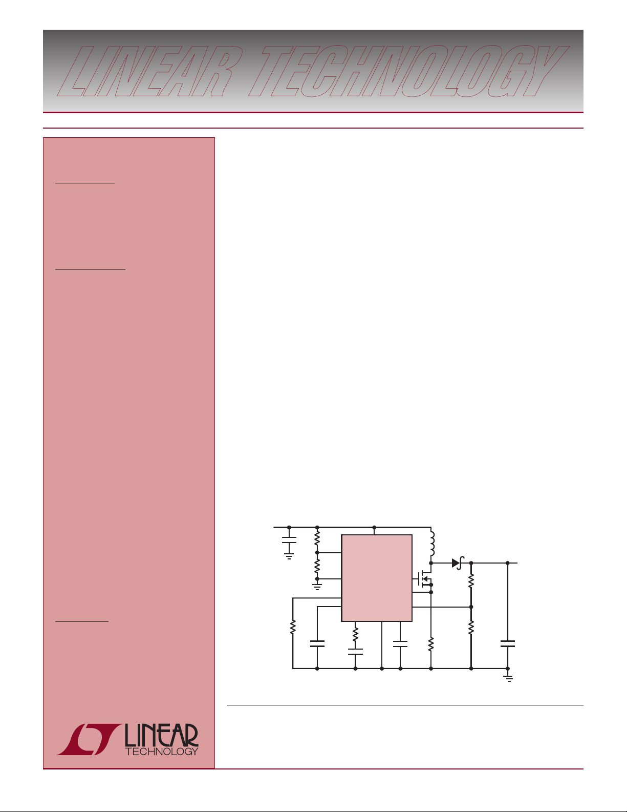
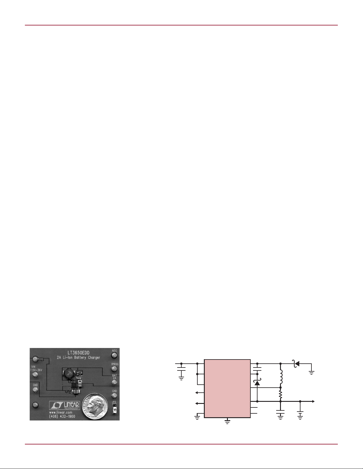
Two New Controllers for Boost, Flyback, SEPIC and Inverting DC/DC Converters Accept Inputs up to 100V
Introduction
Two new versatile DC/DC controller
ICs, the LT®3757 and LT3758, are
optimized for boost, flyback, SEPIC
and inverting converter applications.
The LT3757 operates over an input
range of 2.9V to 40V, suitable for applications from single-cell lithium-ion
battery portable electronics up to high
voltage automotive and industrial
power supplies. The LT3758 extends
the input voltage to 100V, providing
flexible, high performance operation
in high voltage, high power telecommunications equipment. Both ICs
exhibit low shutdown quiescent cur -
rent of 1µA, making them an ideal fit
for battery-operated systems.
Both integrate a high voltage, low
dropout linear (LDO) regulator. Thanks
to a novel FBX pin architecture, the
LT3757 and LT3758 can be connected
directly to a divider from either the
positive output or the negative output to ground. They also pack many
popular features such as soft-start,
input undervoltage lockout, adjustable frequency and synchronization
in a small 10-lead MSOP package or
a 3mm × 3mm QFN package.
by Wei Gu
continued on page 3
Space-Saving, Dual Output
DC/DC Converter Yields
Plus/Minus Voltage Outputs
with (Optional) I2C Programming .......22
Mathew Wich
DESIGN IDEAS
....................................................26–36
(complete list on page 26)
New Device Cameos ...........................37
Design Tools ......................................39
Sales Offices .....................................40
L
, Li nea r E xpr ess , L ine ar Te chn olo gy, L T, LTC , L T M, Bo de CAD , B urs t M ode , F ilt erC AD, L T spi ce,
OPTI-LOOP, Over-The-Top, PolyPhase, SwitcherCAD, µModule and the Linear logo are registered trademarks of Linear
Technology Corporation. Adaptive Power, Bat-Track, C-Load, DirectSense, Easy Drive, FilterView, Hot Swap, LTBiCMOS,
LTCMOS, LinearView, Micropower SwitcherCAD, Multimode Dimming, No Latency ∆Σ, No Latency Delta-Sigma, No R
Operational Filter, PanelProtect, PowerPath, PowerSOT, SafeSlot, SmartStart, SNEAK-A-BIT, SoftSpan, Stage Shedding,
Super Burst, ThinSOT, TimerBlox, Triple Mode, True Color PWM, UltraFast and VLDO are trademarks of Linear Technology
Corporation. All other trademarks are the property of their respective owners.
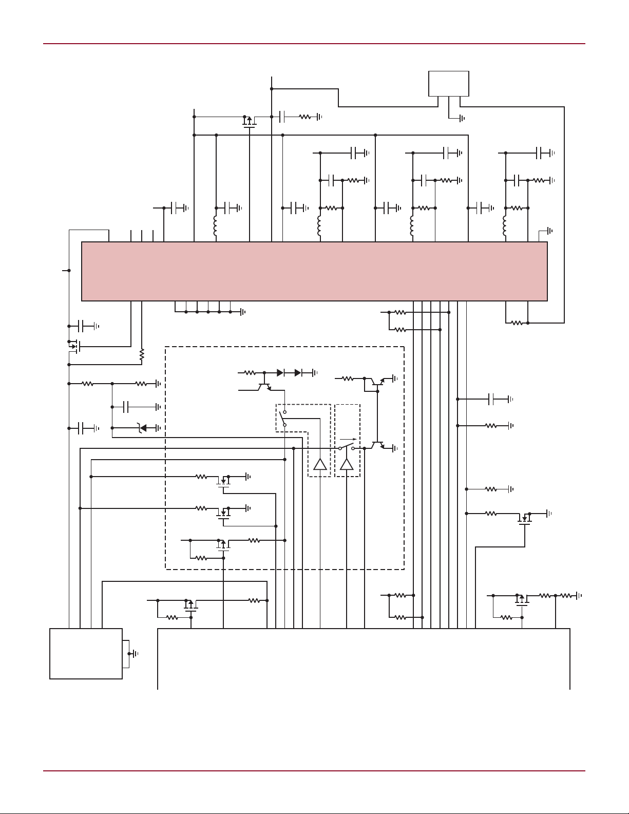
Figure 1. A 10V–30V input, 48V at 1A output boost converter
SENSE
,
L LINEAR IN THE NEWS
Linear in the News…
EDN Innovation Award Winners
EDN magazine on March 30 announced the winners of their
annual Innovation Awards. Linear Technology’s LTM®4606
Ultralow EMI, 6A DC/DC µModule® Regulator was selected
as the winner in the Power ICs: Modules category. This
innovative device significantly reduces switching regulator noise by attenuating conducted and radiated energy
at the source. The µModule device is a complete DC/DC
system-in-a-package, including the inductor, controller IC,
MOSFETs, input and output capacitors and the compensation circuitry—all in a surface mount plastic package
in an IC form factor.
The other Innovation Award winner, in the category
Best Contributed Article, was Jim Williams for his article,
“High Voltage, Low-Noise DC/DC Converters,” which you
can read at www.edn.com/jimwilliams.
In addition to these winners, two other Linear Technology products were finalists for Innovation Awards:
q
LTC®6802 Battery Stack Monitor in the Battery ICs
Category
q
LTC3642 50mA Synchronous Step-Down Converter
in the Power ICs Category
Current Source Makes Worldwide Debut
Linear Technology has just introduced an elegant building-block component that promises to simplify many
power designs—the LT3092 2-terminal current source.
The LT3092 has recently been announced worldwide in a
series of articles by Linear Technology CTO Bob Dobkin.
The LT3092 is a new solution to an old problem: how
to create an easy-to-use current source that maintains
regulation in a variety of conditions. In the past, a designer
would have to choose between an imprecise IC solution,
or build a current source from discrete components.
The LT3092 200mA 2-terminal current source solves
the problems of prior approaches, with its wide voltage
range, high AC and DC impedance, good regulation, low
temperature coefficient, and the fact that it requires no
capacitors. The device’s two floating terminals make it
eminently easy to use.
easy, but it is fraught with problems. Although high quality
voltage sources are readily available, the current source
as an IC has, until now, remained elusive.
set of issues, especially if high accuracy and stability over
temperature are required features. A current source must
operate over a wide voltage range, have high DC and AC
impedance when connected in series with unknown reactance, and exhibit good regulation and a low temperature
coefficient. For optimal 2-terminal solutions, no power
supply bypass capacitor should be used since it degrades
AC impedance.
than 1% initial accuracy and a very low temperature coefficient. Output currents can be set from 0.5mA to 200mA,
and current regulation is typically 10ppm per volt. The
LT3092 operates down to 1.5V or up to 40V. This gives an
impedance of 100MΩ at 1mA or 1 MΩ at 100mA. Unlike
almost any other analog integrated circuit, special design
techniques have been used for stable operation without a
supply bypass capacitor, allowing the LT3092 to provide
high AC impedance as well as high DC impedance. Transient and start-up times are about 20µs.
Linear Announces
New Quad PSE Controller for PoE+
Last month, Linear Technology held press meetings in the
US, Europe and Asia to introduce the LTC4266, a 4-port
Power over Ethernet (PoE) controller for Power Sourcing
Equipment (PSE), designed to meet the IEEE 802.3at requirements of 25.5W or proprietary higher power levels.
Next-generation PoE applications call for more power to
support demanding features, while increasing power efficiency in an effort to be more green and reduce costs.
cabling and is fully compliant with the new IEEE 802.3at
PoE+ standard and backward compatible with the prior
IEEE 802.3af PoE standard. To help conserve power, the
LTC4266 delivers the lowest-in-industry heat dissipation
by using low R
eliminating the need for expensive heat sinks and providing a more robust PSE solution.
plications, including next-generation switches, routers,
hubs and midspans. Users will appreciate the extremely
low power dissipation, which simplifies thermal design
when compared to designs that use PSEs with more fragile,
normally higher R
On the surface, current source design appears relatively
The desirable 2-terminal current source brings its own
The LT3092 meets these expectations. It has better
The LTC4266 provides up to 100W over 4-pair Ethernet
MOSFETs and 0.25Ω sense resistors,
DS(ON)
The LTC4266 is suitable for a wide variety of PSE ap-
, MOSFETs.
DS(ON)
L
2
2
Linear Technology Magazine • June 2009
DESIGN FEATURES L
EFFICIENCY (%)
I
LOAD
(mA)
200
98
93
300 400 500 600 700 800 900 1000
94
94
95
95
96
VIN = 12V
V
IN
= 24V
SENSE
LT3757
V
IN
V
IN
4.5V TO 36V
4.7µF
50V
X5R
4.7µF
10V
X5R
10µF
50V
X5R
C1
22µF
50V
V
OUT
–5V
3A
0.01Ω
M1
Si7850
42.2k
GATE
FBX
GND
INTV
CC
SHDN/UVLO
SYNC
RT
SS
V
C
215k
100k
0.1µF
10nF
8.45k
L1
6.8µH
L2
6.8µH
D1
PDS1045
C1: SANYO 50CE22BS
L1, L2: VISHAY IHLP4040DZ-11
105k
1%
20k
1%
100µF
6.3V, X5R
s2
+
EFFICIENCY (%)
I
LOAD
(mA)
0
88
86
72
500 1000 1500 2000 2500 3000
74
76
82
78
80
84
VIN = 5V
V
IN
= 12V
V
IN
= 36V
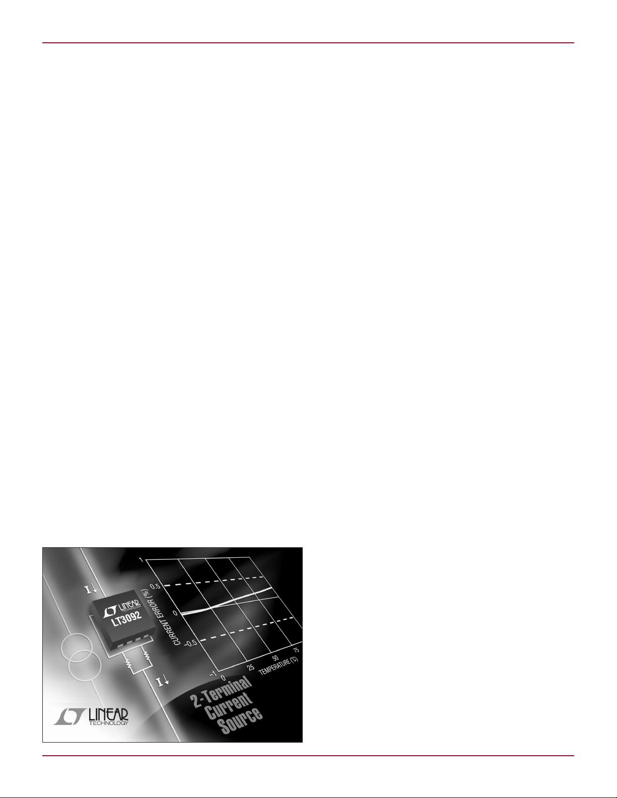
LT3757/58, continued from page 1
Internal High Voltage LDO
In high voltage applications, the
LT3757 and LT3758 eliminate the
need for an external regulator or a
slow-charge hysteretic start scheme
through the integration of an onboard
linear regulator, allowing simple
start-up and biasing. This regulator
generates INTVCC, the local supply
that runs the IC from the converter
input VIN. The internal LDO can operate the IC continuously, provided
the input voltage and/or MOSFET
gate charge currents are low enough
to avoid excessive power dissipation
in the part.
When the INTVCC pin is driven
externally above its regulated voltage
during operation—from the input,
the output or a third winding—the
internal LDO is automatically turned
off, reducing the power dissipation in
the IC. The LDO also provides internal
current limit function to protect IC
from excessive on-chip power dissipation. The current limit decreases
as VIN increases. If the current limit
is exceeded, the INTVCC voltage falls
and triggers the soft-start.
Sensing Output Voltage
Made Easier
Unlike traditional controllers, which
can only sense positive outputs, the
LT3757 and LT3758 have a novel FBX
pin architecture that simplifies the
design of inverting and non-inverting
converters. The LT3757 and LT3758
each contain two internal error amplifiers; one senses positive outputs
and the other negative. When the
converter starts switching and the
output voltage starts ramping up or
down, depending on the topologies,
one of the error amplifiers seamlessly
takes over the feedback control, while
the other becomes inactive.
The FBX pin can be connected
directly to a divider from either a
positive output or a negative output.
This direct connection saves space and
expense by eliminating the traditional
glue circuitry normally required to
level-shift the feedback signal above
ground in negative converters. The
power supply designer simply decides
the output polarity he needs, the topology he wants to use and the LT3757
or LT3758 does the rest.
Precision UVLO Voltage
and Soft-Start
Input supply UVLO for sequencing
or start-up over-current protection is
easily achieved by driving the UVLO
with a resistor divider from the VIN
supply. The divider output produces
1.25V at the UVLO pin when VIN is at
the desired UVLO rising threshold voltage. The UVLO pin has an adjustable
input hysteresis, which allows the IC
to resist a settable input supply droop
before disabling the converter. During
a UVLO event, the IC is disabled and
VIN quiescent current drops to 1µA
or lower.
Figure 2. Efficiency of the
converter in Figure 1
The SS pin provides access to the
soft-start feature, which reduces the
peak input current and prevents output voltage overshoot during start-up
or recovery from a fault condition. The
SS pin reduces the inrush current by
not only lowering the current limit but
also reducing the switching frequency.
In this way soft-start allows the output
capacitor to charge gradually towards
its final value.
Adjustable/Synchronizable
Switching Frequency
The operating frequency of the LT3757
and LT3758 can be programmed from
100kHz to 1MHz range with a single
resistor from the RT pin to ground, or
synchronized to an external clock via
the SYNC pin.
The adjustable operating frequency
allows it to be set outside certain
frequency bands to fit applications
that are sensitive to spectral noise.
Linear Technology Magazine • June 2009
Figure 3. A 4.5V–36V to –5V at 3A inverting converter
Figure 4. Efficiency of the
converter in Figure 3
3
L DESIGN FEATURES
SENSE
LT3758
V
IN
V
IN
18V TO 72V
C
IN
1µF
× 2
INTV
CC
C
OUT
100µF
× 2
V
OUT
–3.3V
2A
0.04Ω
M1
Si4848
36.5k
GATE
FBX
GND
SHDN/UVLO
SYNC
RT
SS
V
C
t
t
t
105k
8.66k
0.1µF
10k
2.2nF
T1
PA1277NL
BAS516
BAV21W
D1
UPS840
31.6k
10k
4.7nF
4.7µF
10k
51.1Ω
EFFICIENCY (%)
LOAD CURRENT (mA)
100
95
55
200 300 400 500 600 700 800 900 1000
60
70
85
75
80
90
VIN = 18V
V
IN
= 24V
V
IN
= 36V
V
IN
= 48V
V
IN
= 72V
SENSE
LT3758
V
IN
V
IN
18V TO 72V
4.7µF
100V
V
OUT
24V
1A
0.02Ω
M1
FDMS2572
42.2k
GATE
FBX
GND
INTV
CC
SHDN/UVLO
SYNC
RT
SS
V
C
•
•
232k
20k
0.1µF
100pF
2.2µF
100V
4.7nF 4.7nF
30.9k
L1B
L1A
WURTH 744 870 470
D1
PDS3100
280k
1%
20k
1%
C
OUT1
22µF
35V
x2
C
OUT2
3.3µF
25V, X5R
+
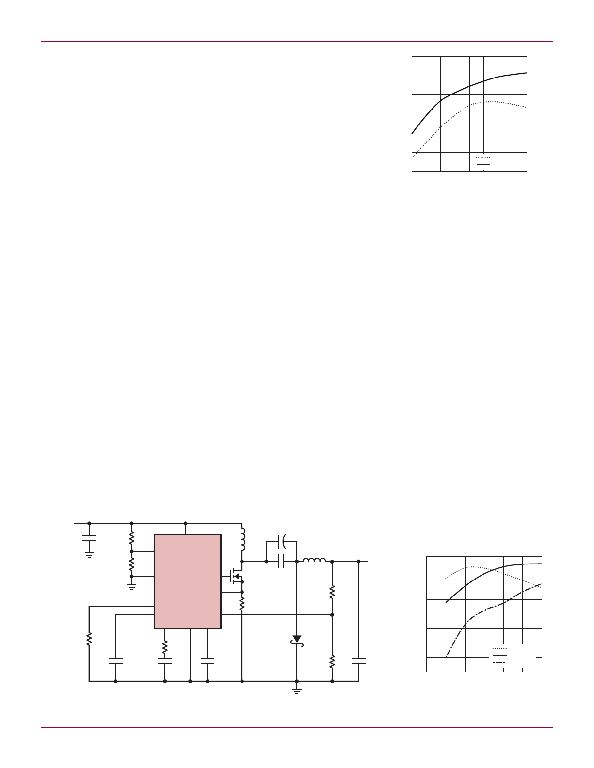
Figure 5. A 18V–72V input, 24V/1A output SEPIC converter
Figure 6. Efficiency of the
converter in Figure 5
In space constrained applications,
higher switching frequencies can be
used to reduce the overall solution
size and the output ripple. If power
loss is a concern, switching at a lower
frequency reduces switching losses,
improving efficiency.
Current Mode Control
The LT3757 and LT3758 use a current mode control architecture to
enable a higher supply bandwidth,
thus improving response to line and
load transients. Current mode control
also requires fewer compensation
components than voltage mode control architectures, making it much
easier to compensate over all operating
conditions.
A 10V–30V Input, 48V/1A
Output Boost Converter
Figure 1 shows a 48V, 1A output
converter that takes an input of 10V
to 30V. The LT3757 is configured as
a boost converter for this applications
where the converter output voltage
is higher than the input voltage.
Figure 2 shows the efficiency for this
converter.
A 4.5V–36V Input, –5V/3A
Output Inverting Converter
Figure 3 shows the LT3757 in an inverting converter that operates from a
4.5V to 36V input and delivers 3A to
a –5V load. The negative output can
be either higher or lower in amplitude
than the input. It has output short-
4
circuit protection, which is further
enhanced by the frequency foldback
feature in the LT3757. The 300kHz
operating frequency allows the use of
small inductors. The ceramic capacitor
used for the DC coupling capacitor provides low ESR and high RMS
current capability. The output power
can easily scaled by the choice of the
components around the chip without
modifying the basic design. Figure 4
shows the efficiency for this converter
at different input voltages.
An 18V–72V Input, 24V/1A
Output SEPIC Converter
A SEPIC converter is similar to the
inverting converter in that it can step
up or step down the input, but with
a positive output. It also offers output
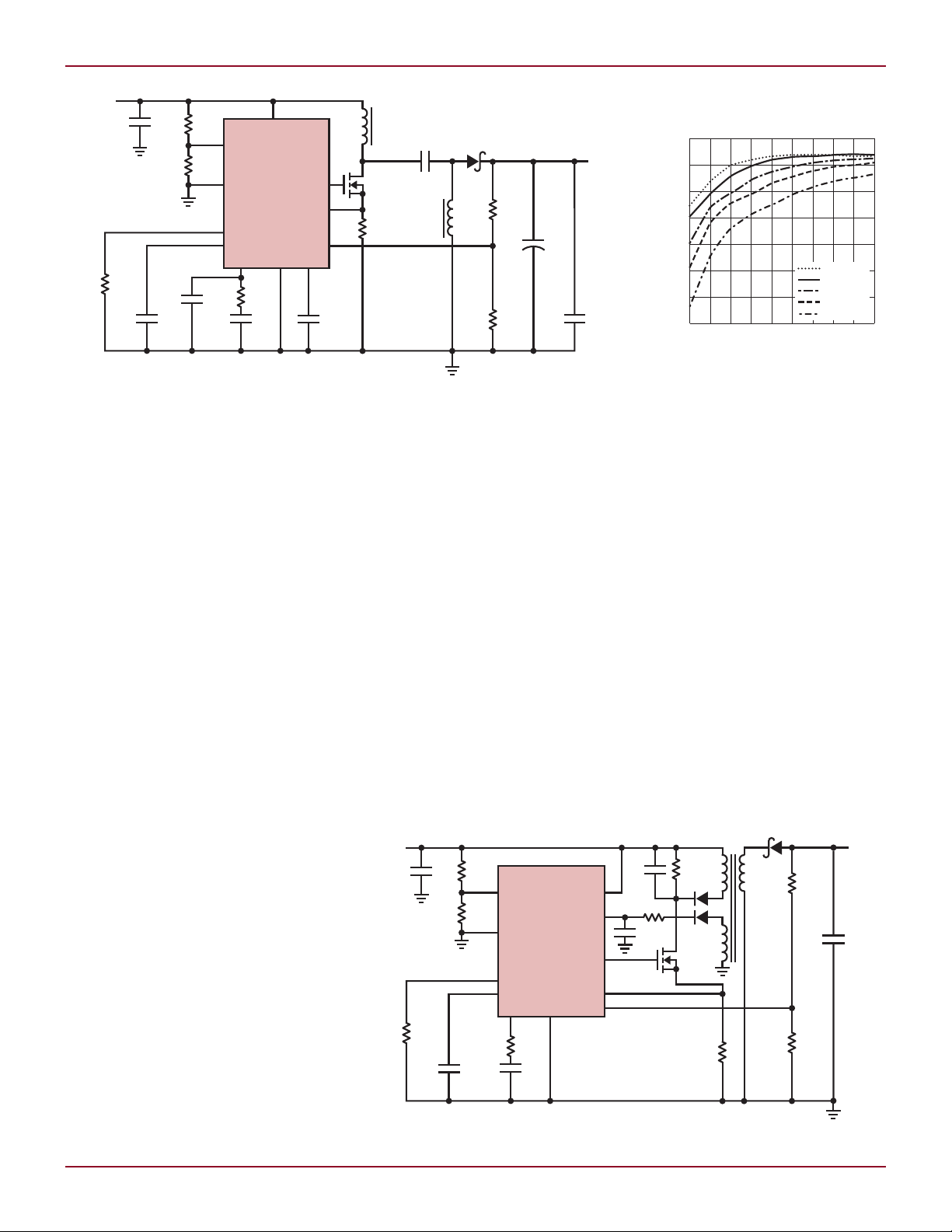
Figure 7. 18V–72V input, –3.3V/2A output flyback converter
disconnect and short-circuit protection. Figure 5 illustrates an 18V–72V
input, 24/1A output SEPIC power
supply using LT3758 as the controller.
Figure 6 shows the efficiency for this
converter at different input voltages.
An 18V–72V Input, –3.3V/2A
Output Flyback Converter
Figure 7 shows the LT3758 in a nonisolated flyback converter with an
18V to 72V input voltage range and a
–3.3V / 2A output. It provides robust
output short-circuit protection thanks
to the frequency foldback feature in the
LT3758. The circuit can also be used
for different negative voltages simply
by changing the value of the resistor
divider on the FBX pin.
continued on page 21
Linear Technology Magazine • June 2009
DESIGN FEATURES L
SW
V
IN
V
IN
7.5V TO 32V
(40 MAX)
CLP
RNG/SS
BOOST
SENSE
BAT
NTC
TIMER
CMPSH1-4
CMSH3-40MA
1µF
10µF
6.8µH
0.05Ω
10µF
LT3650-4.2
Li-Ion
CELL
+
SHDN
CHRG
FAULT
GND
Charge Li-Ion Batteries Directly from High Voltage Automotive and Industrial Supplies Using Standalone Charger in a 3mm × 3mm DFN
Introduction
Growth of the portable electronics
market is in no small part due to the
continued evolution of battery capacities. For many portable devices,
rechargeable Li-Ion batteries are the
power source of choice because of their
high energy density, light weight, low
internal resistance, and fast charge
times. Charging these batteries safely
and efficiently, however, requires
a relatively sophisticated charging
system.
One additional problem faced by
battery charger designers is how to deal
with relatively high voltage sources,
such as those found in industrial
and automotive applications. In these
environments, system supply voltages exceed the input ranges of most
charger ICs, so a DC/DC step-down
converter is required to provide a local
low voltage supply for the charger IC.
The LT3650 standalone monolithic
switching battery charger does not
need this additional DC/DC converter.
It directly accepts input voltages up to
40V and provides charge currents as
high as 2A. It also includes a wealth
of advanced features that assure safe
battery charging and expand its applicability.
The LT3650 includes features that
minimize the overall solution size,
requiring only a few external components to complete a charger circuit. A
fast 1MHz switching frequency allows
the use of small inductors, and the IC
is housed inside a tiny 3mm × 3mm
DFN12-pin package. The IC has builtin reverse current protection, which
blocks current flow from the battery
back to the input supply if that supply
is disabled or discharged to ground,
so a single-cell LT3650 charger does
not require an external blocking diode
on the input supply.
A Charger Designed for
Lithium-Ion Batteries
A Li-Ion battery requires constantcurrent/constant-voltage (CC/CV)
charging system. A Li-Ion battery
is initially charged with a constant
current, generally between 0.5C and
1C, where C is the battery capacity
in ampere-hours. As it is charged,
the battery voltage increases until
it approaches the full-charge float
voltage. The charger then transitions
into constant voltage operation as
the charge current is slowly reduced.
The LT3650-4.1 and LT3650-4.2 are
designed to charge single-cell Li-Ion
by Jay Celani
batteries to float voltages of 4.1V and
4.2V, respectively. The LT3650-8.2
and LT3650-8.4 are designed to charge
2-cell battery stacks to float voltages
of 8.2V and 8.4V.
Once the charge current falls below
one tenth of the maximum constant
charge current, or 0.1C, the battery
is considered charged and the charging cycle is terminated. The charger
must be completely disabled after
terminating charging, since indefinite
trickle charging of Li-Ion cells, even at
miniscule currents, can cause battery
damage and compromise battery stability. A charger can top-off a battery
by continuing to operate as the current falls lower than the 0.1C charge
current threshold to make full use of
battery capacity, but in such cases a
backup timer is used to disable the
charger after a controlled period of
time. Most Li-Ion batteries charge fully
in three hours.
The LT3650 addresses all of the
charging requirements for a Li-Ion
battery. The IC provides a CC/CV
charging characteristic, transitioning
automatically as the requirements of
the battery change during a charging
cycle. During constant-current operation, the maximum charge current
Figure 1. An LT3650 standalone battery
charger is small and efficient.
Linear Technology Magazine • June 2009
Figure 2. A single-cell 2A Li-Ion battery charger configured for C/10 charge termination
5

L DESIGN FEATURES
I
BAT
(A)
0
EFFICIENCY (%)
80
90
100
70
60
0.5
1
1.5
2
VIN = 12V
VIN = 20V
V
BAT
(V)
CHARGE CURRENT (A)
1.0
1.2
1.4
1.6
1.8
2.0
0.6
0.8
0
0.2
0.4
3.0 3.22.6 2.8
3.4
3.8 4.0 4.23.6
FAULT
CHG
V
IN
10k
10k
LT3650
Figure 3. Battery charge current vs BAT pin
voltage for the charger shown in Figure 2
provided to the battery is programmable via a sense resistor, up to a
maximum of 2A. Maximum charge
current can also be adjusted using the
RNG/SS pin. The charger transitions
to constant-voltage mode operation as
the battery approaches the full-charge
float voltage. Power is transferred
through an internal NPN switch element, driven by a boosted drive to
maximize efficiency. A precision SHDN
pin threshold allows incorporation
of accurate UVLO functions using a
simple resistor divider.
Charge Cycle Termination
and Automatic Restart
A LT3650 charger can be configured
to terminate a battery charge cycle
using one of two methods: it can use
low charge current (C/10) detection,
enabled by connecting the TIMER
pin to ground, or terminate based on
the onboard safety timer, enabled by
connecting a capacitor to the TIMER
pin. After termination, a new charge
cycle automatically restarts should
the battery voltage fall to 97.5% of the
float voltage.
is selected, the LT3650 terminates
a charging cycle when the output
current has dropped to 1/10 of the
6
When C/10 ter mination mode
Figure 5. Visual charger status is
easily implemented using LEDs
A Basic Charger
Figure 2 shows a basic 2A single-cell
Li-Ion battery charger that operates
from a 7.5V to 32V input. Charging is
suspended if the input supply voltage
exceeds 32V, but the IC can withstand
input voltages as high as 40V without
damage. The 2A maximum charge
current corresponds to 100mV across
the 0.05Ω external sense resistor. This
basic design does not take advantage
of the status pins, battery temperature
Figure 4. Power conversion efficiency vs
charger output current (I
charger shown in Figure 2
) for the battery
BAT
programmed maximum. In a 2A
charger, for example, the charge cycle
terminates when the battery charge
current falls to 200mA.
Timer termination, or top-of f
charging, is enabled when a capacitor is connected to the TIMER pin.
The value of the capacitor sets the
safety timer duration—0.68µF corresponds to a 3-hour cycle time. When
timer termination is implemented,
the charger continues to operate in
constant-voltage mode when charge
currents fall below C/10, allowing additional low current charging to occur
until the timer cycle has elapsed, thus
maximizing use of the battery capacity.
During top-off charging, the CHRG
and FAULT status pins communicate
“charge complete.” At the end of the
timer cycle, the LT3650 terminates
the charging cycle.
After charge cycle termination, the
LT3650 enters standby mode where
the IC draws 85µA from the input supply and less than 1µA from the battery.
Both the CHRG and FAULT pins are
high impedance during standby mode.
Should the battery voltage drop to
97.5% of the float voltage, the LT3650
automatically restarts and initializes
a new charging cycle.
Table 1. Status pin state and corresponding operating states
CHRG FAULT Charger Status
High Impedance High Impedance Standby/Shutdown/Top-off
Low High Impedance CV/CC Charging (>C/10)
High Impedance Low Bad Battery Detected
Low Low Temperature Fault
monitoring, or a safety timer features.
The battery charging cycle terminates
when the battery voltage approaches
4.2V and the charge current falls to
200mA. A new charge cycle is automatically initiated when the battery
voltage falls to 4.1V.
Safety Features:
Preconditioning,
Bad Battery Detection,
and Temperature Monitor
Li-Ion batteries can sustain irreversible damage when deeply discharged,
so care must be taken when charging
such a battery. A gentle preconditioning charge current is recommended to
activate any safety circuitry in a battery
pack and to re-energize deeply discharged cells, followed by a full charge
cycle. If a battery has sustained damage from excessive discharge, however,
the battery should not be recharged.
Deeply discharged cells can form
copper shunts that create resistive
shorts, and charging such a damaged
battery could cause an unsafe condition due to excessive heat generation.
Should a deeply discharged battery be
encountered, a battery charger must
be intelligent enough to determine
whether or not the battery has sustained deep-discharge damage, and
avoid initiating a full charge cycle on
such a damaged battery.
Linear Technology Magazine • June 2009
DESIGN FEATURES L
CLP
SYSTEM LOAD
INPUT SUPPLY
V
IN
R
CLP
LT3650
SW
V
IN
CLP
RUN/SS
BOOST
SENSE
BAT
NTC
TIMER
1N914
CMSH3-40MA
SYSTEM LOAD
1µF
6.8µH
0.057
LT3650-X
GND
10µF
Li-Ion
CELL
10k
INPUT SUPPLY
12V TO 32V
(40V MAX)
BZX384-C9V1
(9.1V)
10µF
10µF
0.05Ω
SHDN
CHRG
FAULT
10k
36k
3k
10k
0.68µF
+
0.1µF
The LT3650 employs an automatic
precondition mode, which gracefully
initiates a charging cycle into a deeply
discharged battery. If the battery voltage is below the precondition threshold
of 70% of the float voltage, the maximum charge current is reduced to 15%
of the programmed maximum (0.15C)
until the battery voltage rises past the
precondition threshold.
If the battery does not respond
to the precondition current and the
battery voltage does not rise past the
temperature, and suspends charging
should the temperature fall outside of
the safe charging range.
precondition threshold, a full-current
charge cycle does not initiate.
If the safety timer is used for termination, the LT3650 also enables
deep-discharge damage detection
and incorporates a “bad battery”
detection fault. Should the battery
voltage remain below the precondition threshold for 1/8 of the charge
cycle time (typically 22.5 minutes), the
charger suspends the charging cycle
and signals a “bad battery” fault on
the status pins. The LT3650 maintains this fault state indefinitely, but
automatically resets itself and starts
a new charging cycle if the damaged
battery is removed and another battery
is connected.
Li-Ion batteries have a relatively
narrow temperature range where they
can be safely charged. The LT3650
has a provision for monitoring battery
Figure 7. A single cell Li-Ion 2A battery charger with 3 hour safety timer termination, LED status
indicators, temperature sensing, low input voltage charge current foldback, and input supply
current limit
Linear Technology Magazine • June 2009
is enabled by connecting a 10k (B =
3380) NTC thermistor from the IC’s
NTC pin to ground. This thermistor
must be in close proximity to the battery, and is generally housed in the
battery case. This function suspends a
charging cycle if the temperature of the
thermistor is greater than 40°C or less
than 0°C. Hysteresis corresponding to
5°C on both thresholds prevents mode
glitching. Both the CHRG and FAULT
status output pins are pulled low during a temperature fault, signaling that
the charging cycle is suspended. If the
safety timer is used for termination,
the timer is paused for the duration
of a temperature fault, so a battery
receives a full-duration charging cycle,
even if that cycle is interrupted by
the battery being out of the allowed
temperature range.
Figure 6. R
supply current limit
Under/overtemperature protection
sets the input
CLP
Status Indicator Pins
The status of a LT3650 charger is communicated via the state of two pins:
CHRG and FAULT. These status pins
are open-collector pull-down, reporting the operational and fault status of
the battery charger. CC/CV charging
is indicated while charge currents are
greater than 1/10 the programmed
maximum charge current. The status
pins also communicate bad battery
and battery temperature fault states.
Table 1 shows a fault-state matrix for
these two pins.
The status outputs can be used as
digital status signals in processorcontrolled systems, and/or connected
to pull current through an LED for
visual status display. The status pins
can sink currents up to 10mA and can
handle voltages as high as 40V, so a
visual display can be implemented by
simply connecting an LED and series
resistor to VIN.
Maximum Charging Current
Programming and Adjustment
Maximum charge current is set using an external sense resistor placed
between the BAT and SENSE pins of
the LT3650. Maximum charge current
corresponds to 100mV across this resistor. The LT3650 supports maximum
charge currents up to 2A, corresponding to a 0.05Ω sense resistor.
The LT3650 includes two control
pins that allow reduction of the programmed maximum charge current.
The RNG/SS pin voltage directly affects the maximum charge current
such that the maximum voltage allowed across the sense resistor is 1/10
the voltage on RNG/SS for RNG/SS
< 1V. This pin sources a constant
50µA, so the voltage on the pin can
be programmed by simply connecting
a resistor from the pin to ground. A
capacitor tied to this pin generates a
voltage ramp at start-up, creating a
soft-start function. The pin voltage can
be forced externally for direct control
over charge current.
The IC includes a PowerPath™
control feature, activated via the CLP
pin, which acts to reduce battery
charge current should the load on a
continued on page 38
7
16
20
39
+
+
–
+
–
ENABLE
V
IN3
SW3
FB3
GND
37
I
LIM0
30
CHRG
1
CLPROG
3
NTCBIAS
4
NTC
6
OVSENS
V
C
5
OVGATE
38
I
LIM1
11
ENOTG
10
EN1
22
EN2
19
EN3
12
DV
CC
14
SDA
13
SCL
1A 2.25MHz
BUCK
REGULATOR
17
24
25
ENABLE
V
IN2
SW2
FB2
400mA 2.25MHz
BUCK
REGULATOR
23
8
7
ENABLE
V
IN1
29
PROG
32
BAT
15mV
0.3V
3.6V
IDEAL
1.18V
OR 1.15V
+
–
5.1V
SW1
FB1
21
RST3
400mA 2.25MHz
BUCK
REGULATOR
2.25MHz
BIDIRECTIONAL
PowerPath
SWITCHING
REGULATOR
9
D/A
D/A
D/A
4
4
4
I2C PORT
I
LIM
DECODE
LOGIC
CC/CV
CHARGER
3.3V LDO
CHARGE
STATUS
OVP
27
26
28
WALL
DETECT
V
C
CONTROL
31
IDGATE
33
V
OUT
SW
ACPR
WALL
+
–
+
–
+
–
BATTERY
TEMPERATURE
MONITOR
SUSPEND LDO
500µA/2.5mA
36
LDO3V3
2
35
V
BUS
34
V
BUS
L DESIGN FEATURES
Power Management IC Combines USB On-The-Go and USB Charging in Compact Easy-to-Use Solution
by George H. Barbehenn and Sauparna Das
Introduction
The USB interface was originally
designed so that the device providing
power (an “A” device) would act as the
host and the device receiving power (a
“B” device) was the peripheral. The A
plug of the USB cable would always
connect to the host device and the B
plug would connect to the peripheral.
The USB On-The-Go (OTG) standard,
however, removes that restriction, so
that the B device can now become a
host and the A device can act as a
peripheral.
In the USB specification, standard
hosts and hubs are limited to providing
500mA to each downstream device,
but if a device is designated as a USB
charger, it can supply up to 1.5A. USB
chargers come in two flavors. A “dedicated charger” is a charger that is not
capable of data communication with
the attached B device. A ”host/hub
charger” is a charger that is capable
of data communications with attached
B devices.
When USB OTG functionality is
combined with a USB battery charger
in an end-user product, power can
flow in both directions, with relatively
complicated logic and handshaking
steering the flow. To implement a
robust solution, an integrated USB
battery charger and power manager
is a necessity. This article shows how
to use the LTC3576 USB power management IC to easily combine USB
On-The-Go functionality and battery
charger capability into a single portable product.
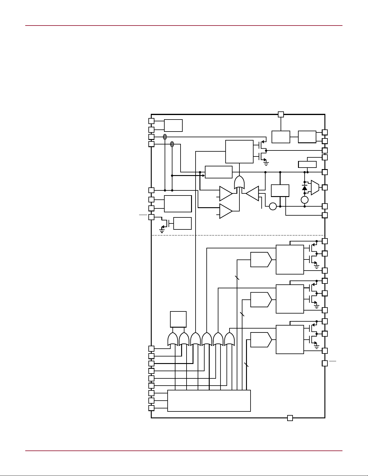
Overview of the LTC3576
The LTC3576 provides the power
resources needed to implement a portable device with USB OTG and USB
battery charger detection capabilities
(see block diagram in Figure 1). The
USB input block contains a bidirec-
8
Figure 1. The LTC3576 combines USB charging and USB On-The-Go by using bidirectional DC/DC
conversion from V
BUS
to V
OUT
Linear Technology Magazine • June 2009
DESIGN FEATURES L
< 6.5µF
ENOTG
MINI/MICRO A/B
MINI/MICRO A PLUG
OTG
COMPATIBLE
DEVICE SUCH
AS LTC3576
OTG
COMPATIBLE
BUSS
TRANSCEIVER
A DEVICE
B DEVICE
MINI/MICRO A/B
MINI/MICRO A PLUG
ENOTG
OTG
COMPATIBLE
DEVICE SUCH
AS LTC3576
OTG
COMPATIBLE
BUSS
TRANSCEIVER
VBUS
D+
D–
ID
GND
VBUS
D+
D–
ID
GND
3.3V
FOR LOW SPEED
ONLY
FOR FULL/HIGH SPEED
ONLY
3.3V
< 6.5µF
ATTACH PHASE
PHYSICAL CONNECTION
OF DEVICES
CONNECT PHASE
DETECT VOLTAGE LEVELS ON
D+/D– TO DETERMINE DATA
SPEED AND POWER LEVELS
ENUMERATION PHASE
SOFTWARE
HANDSHAKE
Figure 2. USB On-The-Go system diagram
Figure 3. USB sequence of events at start-up
tional switching regulator between
V
BUS
from the USB input, this regulator operates as a step-down converter. Using
the Bat-Track™ charging technique,
the switching regulator sets the voltage at V
very efficient charging solution. When
operating as an OTG A device, the
regulator acts as a step-up converter
by taking power from V
5V on V
The LTC3576 also has overvoltage
protection and can be used with an
external HV Buck regulator to provide
V
OUT
switching regulator can take power
from the HV buck regulator to supply
power to the USB connection.
In addition, the LTC3576 provides
two 400mA and one 1A step-down
1.5kΩ to 3.3V on D– during Connect for
1.5kΩ to 3.3V on D+ during Connect for
Full/High Speed, measure voltage on D–
Linear Technology Magazine • June 2009
and V
. When power is coming
OUT
OUT
BUS
to V
.
+ 0.3V, providing a
BAT
OUT
to produce
. In OTG mode, the bidirectional
Table 1. Load power signaling during Attach and Connect
Voltage on D–
with VDAT_SRC on D+ during Attach
Low Speed, measure voltage on D+
switching regulators for generating
three independent voltage rails for the
portable device. The LTC3576 allows
all three step-down switching regulator
output voltages to be enabled/disabled
and adjusted over a 2:1 range via I2C.
All three step-down regulators feature
pulse-skipping mode, Burst Mode
®
operation and LDO mode, which can
also be adjusted on-the-fly via I
2
C.
Mode Detection
The USB specification allows for a
number of different modes of operation
for products supporting both the USB
OTG specification1 and the battery
charger specification2. Figure 2 shows
a typical OTG system and Figure 3
shows the sequence of events that
occur when the USB cable is plugged
in. The product can be a B device
I
BUS
Host/Hub
< 500mA
0V 0.5V–0.7V 0.5V–0.7V
— > 2V < 0.8V
— > 2V < 0.8V
Dedicated Charger
I
BUS
< 1.5A
and can draw up to 100mA, 500mA,
900mA or 1.5A, depending on the type
of A device powering V
, as shown
BUS
in the Table 1.
When an OTG device has a micro/
mini-A plug connected to its micro/
mini-AB connector, the OTG device
becomes the A device and starts off as
the host. The OTG A device supplies
power to V
, as any other host A
BUS
device would, when requested by an
attached peripheral or OTG B Device.
As an A device, the LTC3576 can supply up to 500mA
The USB OTG specification provides
two means for a B device to signal to
the A device that it wants power. The
B device may drive the V
line above
BUS
2.1V, momentarily, or it may signal
by driving the D+ or D– signal lines.
The D+/D– signaling method could be
Host/Hub Charger
I
< (LS,FS < 1.5A/HS < 0.9A)
BUS
9
L DESIGN FEATURES
R5
7.68k
C
C1
1500pF
V
PROCESSOR
M3
UNLESS NOTED, RESISTORS: OHMS, 0402 1% 1/16 WATT
* THREE 1Ω, 5% RESISTORS IN PARALLEL
CAPACTORS: µF, 0402, 10% 25V
D2, D3: 1N4148
L1: 1098AS-2R0M
L2, L3: 1098AS-4R7M
L4: LPS4018-3R3MLC
M2, M3, M6: NDS0610
M4, M5, M7: 2N7002L
Q1, Q2, Q3: MMBT3904LT1
DV
CC
4.35V TO 5.5V
NON-OPERATING FAULT TOLERANCE
TO 30V CONTINUOUS
47k
10k
100k 100k
VBUS
D–
D+
IO
GNDSHGND
IDPUEN
FSPUEN
VBATVEN
VBATV
1ACHARGEEN
BAT
J2
DF3-3P-2DSA
GND
NTC-EXT
V
PROCESSOR
M2
V
PROCESSOR
V
PROCESSOR
V
PROCESSOR
V
PROCESSOR
3.6V AT
400mA
V
BUS
47k 15k 15k
V
BAT
M6
M7
47k
2.00k 2.00k
10k
10k
M4
BATTERY CHARGER HANDSHAKE
M5
U2B
LTC202
Q1
Q3
44.2k
D2
D3
100k
100k
100k
LEAKAGE
CURRENT
MUST BE
<400nA
6.2k
PROGV
CLPROGV
SCL
SDA
DV
CC
RST3
CHRG
VDAT_SRCEN
IDAT_SINKEN
D-V
VBUSV
D–
D+
HUBEN
IDV
DV
CC
I
DAT_SINK
V
DAT_SRC
4.7k
4.7k
100k
1.5k
3.01k
4.7µF
50V
22µF
6.3V
1µF
10V
22µF
6.3V
10µF
6.3V
0.1µF
16V
3.3V
U2A
LTC202
“V” SUF FIX
INDICATES
A/D INP UT
VC
WALL
ACPR
LD03V3
OVSENS
OVGATE
ILM0
ILM1
V
BUS
ENOTG
EN1
EN2
EN3
V
OUT
V
OUT
V
BAT
SW
IDGATE
BAT
V
IN1
SW1
FB1
CHRG
RST3
DVCC
SDA
SCL
CLPROG
PROG
NTCBIAS
NTC
M1
Si2306BDS
M8
Si2333DS
100µF
6.3V
0.337*
U1
LTC3576EUFE
L4
3.3µH
LEAKAGE CURRENT MUST BE < 50nA
0.1µF
16V
L3
4.7µH
2.2µF
6.3V
1.02M
324k
12pF
50V 5%
3.3V AT
400mA
10µF
6.3V
V
IN2
SW2
FB2
L2
4.7µH
2.2µF
6.3V
1.02M
R23
324k
18pF
50V 5%
1.8V
AT1A
22µF
6.3V
V
IN1
SW3
FB3
GND
L1
2.0µH
2.2µF
6.3V
402k
324k
27pF
50V 5%
Q2
J1
USBMICRO-AB
µC
10
Figure 4. Portable system with OTG and battery charger support
Linear Technology Magazine • June 2009

DESIGN FEATURES L
V
IH
V
(D+ or D–)
V
BUS
V
IL
5V
2.1V
0V
100ms
7.5ms
4.9s
B DEVICE SIGNALING
A DEVICE DELIVERING V
USB
detected by an OTG compatible USB
module on the system microcontroller
(µC ). The V
signaling method could
BUS
be detected via an A/D on the µC.
The LTC3576 bidirectional switching
regulator is then enabled as a step-up
converter (OTG mode) by setting the
appropriate bit in the control registers
via I2C.
Implementing a System
for USB OTG and
Battery Charging
Figure 4 shows an application for a portable device that supports both USB
battery charging and USB OTG.
When IDPUEN is low, the ID pin is
pulled up via R5, and if IDV is > 3V
then it is configured to be a B device.
If IDV is < 0.5V then it is configured
to be an A device. The components
enclosed in the box labeled “battery
charger handshake” enable communication of the power capabilities
depending on whether the portable
device is configured as an A device or
a B device. During the Attach phase,
if the portable device is a B device, it
can apply V
DAT_SRC
D+ line, load the D– line with I
(50µA~150µA), and measure the resultant voltage on D– via D–V. If the
voltage is 0, the A device is a Host/Hub,
if the voltage is V
device is a USB Charger.
During the Connect phase, FSPUEN
is pulled low to apply 3.3V to D+,
indicating a full/high speed device.
At the same time the voltage on the
D– line is read again via D–V. If it is
less than 0.8V, then the A device is a
Host/Hub Charger. If the voltage on
D–V is above 2V, then the A device is
a Dedicated Charger.
Linear Technology Magazine • June 2009
(0.5V~0.7V) to the
DAT_SRC
Figure 5. Session Request Protocol timing reference
then the A
DAT_SINK
For OTG functionality, if the portable device is configured as an A
device, then it must drive V
V
, which in this case is powered
OUT
BUS
from
from the battery. Since the LTC3576
is capable of supplying 500mA as an A
device, the µC asserts HUBEN to indi-
cate it is a Host/Hub. The bidirectional
switching regulator in the LTC3576
is enabled by setting the appropriate
bit in the control registers via the I2C
port. If the B device drawing current
from the V
line goes idle, then the
BUS
OTG A device may turn off the V
voltage to conserve the battery. When
the B device needs the V
voltage
BUS
to be present at some later time, it
can request that the A device again
drive V
by turning the bidirectional
BUS
switching regulator back on. It can do
this by signaling on the D+ or D– lines
or by driving the V
line to > 2.1V
BUS
(see Figure 5).
The Host A device only needs to
respond to one of two SRP signaling
methods. However, since not all USB
engines respond to the D+/D– signaling, the V
line is sensed to check if
BUS
it is higher than 2.1V via the VBUSV
A/D input.
When the portable device’s µC detects that the B device is requesting
power on V
, either by sensing the
BUS
D+/D– signaling or by sensing that
V
has been driven higher than 2.1V,
BUS
it should again turn on the OTG stepup converter in the LTC3576.
The PROG (PROGV) and BAT
(VBATV) pins allow a Coulomb counter
to be implemented in the µC. Reading the BAT voltage requires that the
sensing divider be enabled by setting
VBATVEN low. This ensures that the
sense divider network does not dis-
1
charge the battery when the battery
voltage isn’t being measured.
The default battery charge current has been set to 500mA, but can
be increased to 1A by asserting the
1AchargeEN signal. This turns on M7,
halving the PROG resistance and increasing the charge current. The input
current limit will need to be set to 10X
mode (1A) using the I2C port.
The optional network of C14 and
R27/R28/R29 suppresses ripple on
the BAT pin (and consequently on the
V
BUS
pin) if there is no battery present.
BUS
This ripple can be in the tens of mV.
While this will not damage anything,
it may be desirable to suppress this
signal.
The CLPROG (CLPROGV) and
CHRG signals are often useful for
housekeeping tasks in the µC.
The LTC3576 has an overvoltage
protection function that controls M1,
and protects the system from excessive
voltages on the USB (J1) connector.
Because the A/D is configured to monitor V
, it must also be protected by
BUS
D1 from excessive voltages.
The LDO3V3 regulator is configured
to power the µC in low power mode
(<20mA). When the µC needs to leave
low power mode it first enables Buck
Regulator 2, which will provide up to
400mA.
Conclusion
The LTC3576 is a versatile PMIC
consisting of a bidirectional power
manager, overvoltage protection, three
step-down switching regulators and
a controller for an external high voltage step-down switching regulator.
In conjunction with a few support
components, the LTC3576 allows the
implementation of a complete power
management system for portable devices that support both USB OTG and
USB battery charging.
Bibliography
1
”On-The-Go Supplement to the USB Specification”,
Revision 1.3
2
“Battery Charging Specification”, Revision 1.0
3
www.usb,org/developers/docs
L
11
L DESIGN FEATURES
LTC3101
BUCK-BOOST
LDO
ON/OFF
AC
ADAPTER
USB
or
HOT SWAP OUT
3.xV AT 300 to 800mA
1.xV AT 350mA
1.xV AT 350mA
1.8V AT 50mA
3.xV AT 100mA
x.xV AT 200mA
TRACKING OUT
LI-ION
USB
BAT
Power Management IC with Pushbutton Control Generates Six Voltage Rails from USB or 2 AA Cells Via Low Loss PowerPath Topology
Introduction
As the complexity of portable electronic
devices continues to increase, the demands placed on power supplies, and
their designers, expand dramatically.
Not only must typical power systems
accommodate multiple input sources,
with voltages as low as 1.8V for two
AA cells, but they must also provide
an increasing number of independent
output rails to support a wide range
of requirements—for memory, microprocessors, backlights, audio and RF
components. To further complicate
matters, expanding feature sets add up
to increased power dissipation, making
it important to optimize overall power
system efficiency. This is particularly
challenging given that the constant
drive to minimize the required board
area and profile height of the power
system is at direct odds with improving efficiency.
The LTC3101 addresses all of these
challenges with a single-IC power
management solution that allows a
designer to easily maximize overall
power system efficiency while minimizing space requirements. The LTC3101
can generate six power rails by integrating three synchronous switching
converters, two protected switched
Figure 2. Complete portable power
solution with a 16mm × 19mm footprint
12
by John Canfield
Figure 1. Six output rails, a low loss PowerPath and integrated pushbutton control
power outputs, and an LDO. Its integrated low loss PowerPath™ topology
allows each switching converter to
run directly from either of two input
power sources.
Two 350mA, high efficiency low
voltage rails, typically used to power
processors and memory, are generated
by synchronous buck converters. Each
converter is able to operate down to an
input voltage of 1.8V thereby enabling
single stage conversion from any input
power source.
A single inductor buck-boost
converter generates a high efficiency
intermediate output rail, typically at
3V or 3.3V, and is able to operate from
either input power source and with
input voltages that are above, below,
or even equal to the output regulation
voltage. The buck-boost converter
can supply a 300mA load at 3.3V for
battery voltages down to 1.8V and an
800mA load for input voltages of 3.0V
and greater.
Two always-alive outputs—MAX,
which tracks the higher voltage input
power source and LDO, a fixed 1.8V
output—provide power to critical
functions that must remain powered
under all conditions. An integrated
pushbutton controller with programmable µP reset generator provides
complete ON/OFF control using only
a minimal number of external components while independent enables allow
total power-up sequencing flexibility.
This complete portable power solution
is packaged in a single low profile 24lead 4mm × 4mm QFN package and
the entire power supply, including
all external components, occupies a
PCB area of less than 3cm2 as shown
in Figure 2.
Zero Loss PowerPath
Topology Maximizes
Efficiency
Although rechargeable Li-Ion and
Li-Polymer batteries are the leading
chemistries for powering portable
devices due to their high energy density and long cycle life, many portable
devices continue to be powered by
alkaline and NiMH cells. This allows
indefinite periods of use away from a
Linear Technology Magazine • June 2009

BAT1
USB1
C
RS
ENA1
ENA2
ENA3
PWRKEY
PWRON
PWM
PBSTAT
RESET
USB2
FB3
LDO
SW2
FB2
HSO
MAX
10µF
10µF
2 AA
CELLS
USB/WALL
ADAPTER
1.8V TO 5.5V
10µF
1M
V
OUT3
= 3.3V
300mA FOR VIN ≥ 1.8V
800mA FOR VIN ≥ 3V
221k
Hot Swap OUTPUT: 3.3V AT 100mA
TRACKING OUTPUT: 200mA
4.7µH
4.7µF
1.8V AT 50mA
V
OUT2
1.8V
350mA
V
OUT1
1.5V
350mA
10µF
221k
110k
4.7µH
SW1
FB1
10µF
221k
147k
4.7µH
0.1µF
ON/OFF
BAT2 SW3A
LTC3101
GND
µP
SW3B OUT3
DIS ENA
+
USB
BAT
+
BUCK
V
OUT
USB
BAT
+
BUCK-BOOST
V
OUT
charging socket—which is particularly
important for devices intended for use
in remote locales such as handheld
personal navigation devices or portable
medical devices. Voice recorders, digital still cameras and ultra-small video
recorders are additional examples of
devices that benefit from the ability to
operate from a pair of commonly available batteries, rather than requiring
the lengthy recharging cycle needed
for an internal Li-Ion battery.
Even in portable devices where the
primary power source is restricted
to AA or AAA form factor cells, there
still exist a wide variety of compatible chemistries including alkaline,
rechargeable alkaline, NiMH and
single-use lithium. As a result, the
AA/AAA powered device must accommodate a wide range of input voltages,
from 1.8V for two series alkaline cells
near end of life, to approximately 3.7V
for a pair of fresh non-rechargeable
lithium cells. With its wide 1.8V to
5.5V input voltage range, the LTC3101
can easily support all of these battery chemistries. In addition, the
LTC3101 is able to operate from a
single standard Li-Ion/Polymer cell in
cases where recharging is performed
independently.
Although rechargeable cells are
usually charged outside these types
of devices, the power supply must
accommodate a secondary tethered
power source such as USB or a regulated wall adapter. Consequently, the
power supply must include a means to
generate every power rail from either of
two input sources, and the ubiquitous
3.3V rail must be generated from input
power sources that can be higher or
lower voltage.
In many devices, the capability to
handle dual power sources is provided
by using discrete power MOSFETs to
switch regulator inputs between the
two input power sources or by utilizing
two regulators for generation of each
rail (for example, a buck converter
that generates a 3.3V rail from the
USB input in conjunction with a boost
converter that generates the 3.3V rail
from the battery input).
Both of these approaches suffer
from significant drawbacks. The par-
Linear Technology Magazine • June 2009
allel converter approach increases
system cost and size given that only
one converter is ever active at any given
time and often suffers from glitches
and disruptions to the output rails
during the transition between the
two input power sources. Similarly,
the discrete power switch technique
reduces efficiency due to the addition
of extra series elements in the power
path, increases component count,
and can also lead to disruptions in
the output rails unless the supply
crossover is carefully controlled.
The LTC3101 avoids these problems by using a low loss PowerPath
topology as shown in Figure 4, where
each converter is able to operate directly from either input power source.
In this architecture, each switching
converter utilizes an additional power
switch, which is connected to the
alternate power input. As a result,
each converter is able to run with
maximum efficiency from either input
power source so no efficiency penalty
DESIGN FEATURES L
Figure 3. Typical application
is incurred in supporting dual input
power sources.
The total solution area is minimized
by the fact that the same inductor is
used in either case. In addition, the
automatic transition between the
two input power sources is seamless—there is no interruption to any
of the output rails. Figure 5 shows the
transient response of the buck-boost
converter as the input power source
transitions from battery power to USB
power in response to a live cable plug
into a USB port.
Integrated Buck-Boost
Provides High Efficiency
3V/3.3V Rail from
Any Power Source
In many portable devices an intermediate supply rail, typically regulated to
3.3V, is required to power an RF stage
or audio amplifiers. Often this rail is
generated from the two series AA cells
using a boost converter. However, the
higher cell voltage of single-use lithium
Figure 4. The low loss PowerPath architecture
13

L DESIGN FEATURES
OUTPUT
VOLTAGE
200mV/DIV
INDUCTOR
CURRENT
200mA/DIV
V
USB
2V/DIV
100µs/DIV
batteries such as the Energizer e2
brand can cause problems when the
battery voltage is significantly higher
than the output voltage. Depending
on the boost converter utilized, this
can result in low efficiency operation
or even loss of regulation on the 3.3V
rail.
To avoid this problem, the LTC3101
generates the 3.3V rail utilizing a
buck-boost converter, which accepts
any input voltage in the range 1.8V to
5.5V without sacrificing efficiency. In
fact, when operating with a fresh pair
of single-use lithium batteries at 3.7V,
the LTC3101 buck-boost efficiency is
greater than 94% at 150mA load current. In addition, the same buck-boost
converter is able to operate directly
from the USB input, so generation
of the 3.3V rail requires only a single
inductor.
Reverse Blocking LDO
Enables Data Retention
During Battery Swaps
Many portable electronic devices contain critical circuitry such as real time
clocks, which must remain powered
under all conditions. The MAX and
LDO outputs of the LTC3101 are alive
as long as either input power source
is present, regardless of the state of
the pushbutton interface or enable
inputs. It is also possible to connect
a large capacitor directly to the LDO
output to serve as a charge reservoir
for powering critical functions during
times, such as battery swaps, when
both input power sources are temporarily removed. In its reverse blocking
state, the maximum reverse current
through the LDO is limited to under
1µA in order to preserve charge in the
reservoir capacitor.
Figure 5. Buck-boost output voltage transient on USB hot plug
14
MAX and Hot Swap Outputs
Power Additional Regulators
and Flash Memory Cards
Portable electronic devices often require additional miscellaneous power
supplies, such as current regulated
drivers for LED backlighting and LDOs
for low power rails. Typically these
secondary supplies must be functional
whenever either input power source
is present, so they also require power
path control to switch between the two
input power sources.
External supplies can take advantage of the LTC3101’s PowerPath
control circuit via the MAX output,
which continuously tracks the higher
voltage input power source. Additional
regulators can be directly connected
to this output, thus freeing the designer from the need to implement
an additional switched power path.
The MAX output is able to support a
200mA load and is current limited to
protect against overload conditions
and short circuits.
Many portable electronic devices
provide flash memory card interfaces for use as bulk storage memory.
Typical flash memory cards such as
Compact Flash (CF) and Secure Digital (SD) formats require a regulated
3.3V supply that is typically capable
of providing tens of milliamps. However, many flash memory cards have
a significant amount of supply bypass
capacitance installed on the card and
when hot plugged into a live 3.3V rail,
the inrush current required to charge
these supply bypass capacitors on
the memory card can momentarily
drag down the host’s supply, causing disruption to other ICs powered
by that rail.
The LTC3101’s dedicated 100mA
hot swap output (powered from the
buck-boost converter rail) does not
have this problem. The independent
current limit of the hot swap switch
allows flash memory cards to be hot
plugged without disruption to the
primary 3.3V rail. In addition, the
hot swap output is fully short circuit
protected to safeguard against accidental shorts at the memory card
interface port.
Low Quiescent Current
Minimizes Battery Drain
Most portable electronic devices spend
significant, if not the majority, of their
time in sleep or standby modes. In fact,
even when an appliance is off, there is
often circuitry that must remain powered, including real time clocks and
volatile memory storing configuration
settings. The always-alive 1.8V LDO
and tracking MAX outputs remain
powered whenever either input power
source is present allowing them to be
utilized for supplying such critical
functions. In order to minimize battery
discharge during this time, the total
quiescent current draw of the LTC3101
with both the MAX and LDO outputs
active is reduced to 15µA.
Many portable electronic devices
also support a standby mode in which
several of the system’s voltage rails
must be kept in regulation. Typically,
in standby the microprocessor and
memory remain powered and the
processor is placed in a low current
sleep mode enabling the device to return to an active operating state with
minimal delay.
In order to minimize battery drain
in such modes of operation, all three
switching converters in the LTC3101
feature Burst Mode operation, which
can be enabled via a dedicated pin.
With Burst Mode operation enabled,
the buck converters automatically
transition from PWM to Burst Mode
operation at sufficiently light load
(typically 10mA) while the buck-boost
converter uses Burst Mode operation
at all load currents. In Burst Mode
operation with all six output rails
maintained in regulation the total
quiescent current draw of the LTC3101
Linear Technology Magazine • June 2009

is reduced to only 38µA. In addition,
HSO
(OPTIONAL)
ENA1
ENA2
R
FILT
C
FILT
500µs/DIV
V
OUT
BUCK 1
(1V/DIV)
V
OUT
BUCK 2
(1V/DIV)
V
OUT
BUCK-BOOST
(2V/DIV)
HOT SWAP
(2V/DIV)
500µs/DIV
V
OUT
BUCK 1
(1V/DIV)
V
OUT
BUCK 2
(1V/DIV)
V
OUT
BUCK-BOOST
(2V/DIV)
HOT SWAP
(2V/DIV)
to ensure low supply rail noise, the
Burst Mode operation output voltage
ripple is typically less than 1% of the
regulation voltage of each output rail.
All three switching converters can be
forced into fixed frequency PWM mode
operation to ensure low noise operation while critical system functions
are underway.
DESIGN FEATURES L
Figure 6. Default power-up sequencing
Flexible Power-Up
Sequencing Options
The LTC3101 provides a variety of
sequencing options. Most systems
that incorporate multiple power
supply rails require that they come
into regulation in a certain sequence
with specific timing. This is because
individual ICs and modules that are
powered from multiple rails need
particular sequencing to minimize
start-up current and ensure predictable power-up behavior.
Common examples include microprocessors and FPGAs, which often
require that the peripheral supply
powering the I/O buffers is made
available only after the lower voltage
core is in regulation. In addition, at
the board level, many systems bring
up the supplies for peripheral devices
only after the processor is powered up
to avoid erratic behavior from peripherals lacking processor oversight.
Each switching converter in the
LTC3101 has an internal power-good
comparator, which is used internally
to sense when that rail is in regulation. The default power-up sequence
enables the individual outputs in the
following order: buck converter 1, buck
converter 2, buck-boost converter,
and finally the hot swap output. Each
converter is enabled once the preceding converter in the sequence reaches
regulation (typically 94% of the target
output voltage). The default power-up
sequence using all converter channels
is shown in Figure 6.
If the dedicated enable pin for any
switching converter is held low during
the pushbutton triggered initiation,
that converter is simply skipped in
the default power-up sequence, but
that channel can still be enabled at a
later time. This functionality allows the
LTC3101 to implement any arbitrary
power-up sequence using few if any
external components.
can be accomplished by adding a
simple RC filter with the desired time
constant between the hot swap output
and the buck enables. Notice however,
that if the hot swap output is forced
to ground, the buck converters will
be disabled. If there is a potential for
the hot swap output to fall below the
enable threshold (typically 0.7V) during normal operation, then the buck
enables can instead be driven through
an RC delay from the buck-boost voltage directly rather than from the hot
swap output.
For example, in some systems the
3.3V buck-boost rail must come up
first, followed by both buck rails in
unison. This can be accomplished
by driving the buck enables from the
hot swap output, HSO, as shown in
Figure 7. The bucks do not power up
in the normal sequence since their
enables are low to start. Once the
buck-boost reaches regulation, the hot
swap output is enabled, which in turn
enables the two buck converters. Since
the hot swap output is not powered
until the buck-boost is in regulation,
this configuration ensures that the
buck converters do not become active
until after the buck-boost is in regulation, as shown by the waveforms in
Figure 8.
If an additional delay is required
Conclusion
The LTC3101 is perfectly suited for
the needs of the next generation of
extended functionality compact portable electronic devices.
The job of the power system designer
is simplified by its compact solution
footprint and ability to generate six
commonly required output voltage
rails automatically from two independent wide input voltage range power
sources. The LTC3101’s low quiescent
current and a high efficiency, low loss
PowerPath architecture maximize
battery life. A wide range of output
voltages, programmable duration
µP reset generator, and independent
enables offer flexibility and easy customization.
before the bucks are enabled, this
L
Figure 7. Sequencing the buck enables
using the hot swap output rail
Linear Technology Magazine • June 2009
Figure 8. Power-up sequencing, buck-boost followed by the buck outputs
15

L DESIGN FEATURES
ADC
0.1µF
12V
V
OUT
12V
1.5A
20k
10k
12V
330µF
V
DD
UV
OUT
PG
GND
I
MON
LTC4217DHC-12
INTV
CC
TIMER
FLT
AUTO
RETRY
+
TEMPERATURE (°C)
–50
0.9
0.8
0.7
0.6
0.5
0.4
0.3
–25 0 25 50 75 150125100
V
ISET
(V)
Improve Hot Swap Performance and Save Design Time with Hot Swap Controller that Integrates 2A MOSFET and Sense Resistor
Introduction
The LTC4217 Hot Swap controller
turns a board’s supply voltage on and
off in a controlled manner allowing
the board to be safely inserted and
removed from a live backplane. No surprise there, this is generally what Hot
Swap controllers do, but the LTC4217
has a feature that gives it an advantage over other Hot Swap controllers.
It simplifies the design of Hot Swap
systems by integrating the controller,
MOSFET and sense resistor in a single
IC. This saves significant design time
that would otherwise be spent choosing an optimum controller/MOSFET
combination, setting current limits,
and carefully designing a layout that
protects the MOSFET from excessive
power dissipation.
One significant advantage of an
integrated solution over discrete solutions is that the current limit accuracy
is well known. In discrete solutions, the
overall precision of the current limit
is a function of adding the tolerances
of contributing components, while in
the LTC4217, it appears as a single
2A specification.
The integrated solution also simplifies layout issues by optimizing
MOSFET and sense resistor connections. The inrush current, current
limit threshold and timeout can be
set to default values with no external
16
components or easily adjusted using
resistors and capacitors to better suit a
large range of applications. The part is
able to cover a wide 2.9V to 26.5V voltage range and includes a temperature
and current monitor. The MOSFET
is kept in the safe-operating–area
(SOA) by using a time-limited foldback
current limit and overtemperature
protection.
The LTC4217 can be easily applied
in its basic configuration, or, with a
few additional external components,
set up for applications with special
requirements.
Monitoring the MOSFET
The LTC4217 features MOSFET
current and temperature monitoring. The current monitor outputs a
current proportional to the MOSFET
current, while a voltage proportional
to the MOSFET temperature is available. This allows external circuits to
predict possible failure and shutdown
the system.
The current in the MOSFET passes
through a sense resistor, and the voltage on the sense resistor is converted
to a current that is sourced out the
I
pin. The gain is 50µA from I
MON
for 1A of MOSFET current. The output
current can be converted to a voltage
using an external resistor to drive a
Figure 2. 12V, 1.5A card resident application
by David Soo
Figure 1. V
comparator or ADC. The voltage compliance for the I
(INTVCC – 0.7V).
The MOSFET temperature corresponds linearly to the voltage on the
I
pin, with the temperature profile
SET
shown in Figure 1. The open circuit
voltage on this pin at room temperature
is 0.63V. In addition, the overtemperature shutdown circuit turns off
the MOSFET when the controller die
temperature exceeds 145°C, and turns
it on again when the temperature
drops to 125°C.
12V Application
Figure 2 shows the LTC4217-12 in a
MON
12V Hot Swap application with default
settings. The only external component
required is the capacitor on the INTVCC
pin. The current limit, inrush current
control, and protection timer are internally set at levels that protect the
integrated MOSFET. The input voltage
monitors are preset for a 12V supply
using internal resistive dividers from
the V
pins. The UV condition occurs when
VDD falls below 9.23V; OV when VDD
exceeds 15.05V.
ply voltage on and off in a controlled
supply to drive the UV and OV
DD
The LTC4217 turns a board’s sup-
Linear Technology Magazine • June 2009
vs temperature
ISET
pin is from 0V to
MON

DESIGN FEATURES L
150k
20k
ADC
224k
0.1µF
20k
12V
12V
10k
0.47µF
330µF
V
OUT
12V
0.8A
V
DD
UV
OUT
FB
PG
GND
I
MON
20k
20k
I
SET
0.1µF
1k
GATE
LTC4217FE
OV
INTV
CC
TIMER
FLT
+
140k
20k
FB VOLTAGE (V)
0
0
CURRENT LIMIT VALUE (A)
0.5
1.0
1.5
2.0
2.5
0.2 0.4 0.6 0.8 1.0 1.2
t1 t2
SLOPE = 0.3V/ms
GATE
OUT
VDD + 6.15
V
DD
manner, allowing the board to be
safely inserted and removed from a live
backplane. Several conditions must be
present before the internal MOSFET
can be turned on. First the VDD supply
exceeds its 2.73V undervoltage lockout
level and the internally generated INTVCC crosses 2.65V. Next the UV and
OV pins must indicate that the input
power is within the acceptable range.
These conditions must be satisfied
for the duration of 100ms to ensure
that any contact bounce during the
insertion has ended.
The MOSFET is then turned on by
a controlled 0.3V/ms gate ramp as
shown in Figure 3. The voltage ramp of
the output capacitor follows the slope
of the gate ramp thereby setting the
supply inrush current at:
I
= CL • (0.3V/ms)
INRUSH
To reduce inrush current further,
use a shallower voltage ramp than the
default 0.3V/ms by adding a ramp
Linear Technology Magazine • June 2009
Figure 5. 0.8A, 12V card resident applicaiton
Figure 3. Supply turn-on
capacitor (with a 1k series resistor)
from gate to ground.
As OUT approaches the VDD supply,
the powergood indicator (PG) becomes
active. The definition of power good
is the voltage on the FB pin exceeds
1.235V while the GATE pin is high. The
FB pin monitors the output voltage via
an internal resistive divider from the
OUT pin. Once the OUT voltage crosses
the 10.5V threshold and the GATE to
OUT voltage exceeds 4.2V, the PG pin
ceases to pull low and indicates that
the power is good. Once OUT reaches
the VDD supply, the GATE ramps until
clamped at 6.15V above OUT.
The LTC4217 features an adjustable current limit with foldback that
protects against short circuits or
excessive load current. The default
current limit is 2A and can be adjusted
lower by placing a resistor between the
I
pin and ground. To prevent exces-
SET
sive power dissipation in the switch
during active current limit, the available current is reduced as a function
Figure 4. Current limit threshold foldback
of the output voltage sensed by the FB
pin as shown in Figure 4.
An overcurrent fault occurs when
the current limit circuitry has been
engaged for longer than the delay set
by the timer. Tying the TIMER pin
to INTVCC configures the part to use
a preset 2ms overcurrent time-out
and a 100ms cool-down time. After
the 100ms cool-down, the switch
is allowed to turn on again if the
overcurrent fault has been cleared.
Bringing the UV pin below 0.6V and
then high clears the fault. Tying the
FLT pin to the UV pin allows the part
to self-clear the fault and turn on again
after the 100ms cool-down.
Programmable Features
The LTC4217 application shown in
Figure 5 demonstrates the adjustable
features.
The UV and OV resistive dividers
set undervoltage and overvoltage turnoff thresholds while the FB divider
determines the power good trip point.
The R-C network on the GATE pin
decreases the gate ramp to 0.24V/ms
from the default 0.3V/ms to reduce
the inrush current.
The 20k I
sistive divider with an internal 20k
resistor to reduce the current limit
threshold (before foldback) to onehalf of the original threshold for a 1A
current limit. The graph in Figure 6
shows the current limit threshold as
the I
resistor varies.
SET
As in the previous application, the
UV and FLT signals are tied together
so that the part auto-retries turn-on
following shutdown for an overcurrent
fault.
resistor forms a re-
SET
continued on page 25
17

L DESIGN FEATURES
V
OUT
(AC)
50mV/DIV
V
SW
20V/DIV
I
L
10A/DIV
I
LOAD
10A/DIV
5µs/DIV
LOAD STEP 0A TO 10A
VIN = 12V
V
OUT
= 1.2V
MODE = 0V
SW FREQ = 400kHz
V
OUT
(AC)
50mV/DIV
V
SW
20V/DIV
I
L
10A/DIV
I
LOAD
10A/DIV
5µs/DIV
LOAD STEP 10A TO 0A
VIN = 12V
V
OUT
= 1.2V
MODE = 0V
SW FREQ = 400kHz
Compact No R
SENSE
Controllers
Feature Fast Transient Response
and Regulate to Low V
from Wide Ranging V
Introduction
The trend in digital electronics is to
lower voltages and increasing load currents. This puts pressure on DC/DC
converters to produce low voltages
from increasingly voltage-variable
supplies, such as stacked batteries
and unregulated intermediate power
buses, so power converters must be
optimized for low output voltages, low
duty factors, and wide control bandwidths. To meet these requirements,
the DC/DC controller IC must offer
high voltage accuracy, good line and
load regulation, and fast transient
response. The constant on-time valley current mode architecture used in
the LTC3878 and LTC3879 is ideally
suited to low duty factor operation,
offering a compact solution with excellent system performance.
The LTC3878 and LTC3879 are
a new generation of No R
SENSE
controllers that meet the demanding
requirements of low voltage supplies
for digital electronics. The LTC3878 is
a pin compatible replacement for the
LTC1778 in designs where EXTVCC
is not required. The LTC3879 adds
separate RUN and TRACK/SS pins for
applications requiring voltage tracking. Both devices offer continuously
programmable current limit, using
the bottom MOSFET VDS voltage to
sense current.
Valley Current Mode
Control Simplifies Loop
Compensation…
There are two common implementations of current mode control. Peak
current mode control regulates the
high side MOSFET on-time, while
valley current mode regulates the
bottom side MOSFET off-time. The
current mode loop bandwidth is in-
18
™
Figure 1. Transient response,
positive load step
versely proportional to the on-time for
a peak current controller and inversely
proportional to the off-time for a valley
mode controller. A peak current mode
controller with an on-time of 50ns
must have a closed current loop bandwidth exceeding 20MHz. For a valley
current mode controller, the current
loop bandwidth is determined by the
typical off-time of 220ns, resulting in a
closed current loop bandwidth requirement of only 4.5MHz. Consequently,
valley current mode control has less
stringent bandwidth requirements for
the same system performance when
compared to a peak current mode
control in a similar application. This
allows the LTC3878 and LTC3879 to
offer high performance, low duty factor
operation at reasonable current loop
bandwidths.
The constant on-time valley current
mode control of the LTC3878 and
LTC3879 simplifies compensation
design by eliminating the need for
slope compensation. A fixed frequency
valley mode controller requires slope
compensation when operating at less
than 50% duty factor to prevent subcycle oscillation. Subcycle oscillation
occurs because the PWM pulse width
IN
OUT
by Terry J. Groom
Figure 2. Transient response,
load release
is not uniquely determined by inductor
current alone. This oscillation cannot
exist in constant-on-time control because the PWM pulse width is uniquely
determined by the internal open loop
pulse generator. True current mode
control and constant on-time combine
to give the LTC3878 and LTC3879
performance advantages over other
constant on-time regulators or fixed
frequency valley current mode control
architectures.
…and Improves Transient
Response Time
In a buck controller, transient response
is largely determined by how quickly
the inductor current responds to loop
disturbances. The most demanding
loop disturbances are load steps and
load releases.
The inherent speed advantage of
a constant on-time architecture lies
in the fact that the regulator is pulse
frequency modulated (PFM) insead
of pulse width modulated (PWM).
Although the switching frequency is
fixed in steady state operation, it can
increase or decrease as required in
response to an output load step or
load release.
Linear Technology Magazine • June 2009

DESIGN FEATURES L
f Hz
MAX
ON OFF MIN
t t
=
(
)
+
1
( )
( )
f g EA R
I
C
V
V
CGO m C
LIMIT
OUT
REF
OUT
= • •( )
.1 6
1
I
L
5A/DIV
V
OUT
0.5V/DIV
TRACK/SS
0.5V/DIV
20ms/DIV
VIN = 12V
V
OUT
= 1.2V
SW FREQ = 400kHz
+
TRACK/SS
LTC3879
BOOST
16
C
B
0.22µF
M1
RJK0305DPB
C
VCC
4.7µF
C
C1
220pF
C
C2
33pF
D
B
CMDSH-3
L1
0.56µH
C
OUT1
330µF
2.5V
s2
C
OUT2
47µF
6.3V
s2
+
C
IN1
10µF
50V
s3
C
IN2
100µF
50V
V
OUT
1.2V
15A
V
IN
4.5V TO 28V
1
PGOOD
R
PG
100k
R2
80.6k
R
C
27k
R
FB1
10.0k
R1
10.0k
TG
152
V
RNG
SW
143
MODE PGND
134
I
TH
BG
125
SGND INV
CC
116
I
ON
V
IN
107
V
FB
RUN
98
R
ON
432k
R
FB2
10.0k
M2
RJK0330DPB
C
IN1
: UMK325BJ106MM s3
C
OUT1
: SANYO 2R5TPE330M9 s2
C
OUT2
: MURATA GRM31CR60J476M s2
L1: VISHAY IHLP4040DZ-11 0.56µH
C
SS
0.1µF
LOAD CURRENT (A)
30
EFFICIENCY (%)
90
100
20
10
80
50
70
60
40
0.01 1 10 100
0
0.1
CONTINUOUS
MODE
DISCONTINUOUS
MODE
VIN = 12V
V
OUT
= 1.2V
SW FREQ = 400kHz
The maximum frequency in response to a load step is determined
by the on-time plus the off-time:
In low duty factor applications the
maximum frequency is typically much
greater than the nominal operating frequency, producing excellent transient
characteristics.
Figure 1 shows the load step response of a 12V-to-1.2V converter
operating at 400kHz. In this case the
on-time is equal to 250ns and the
minimum off-time is 220ns. The maximum frequency available to respond
to a load step is 2.12MHz, which is
over five times the nominal switching
frequency. Note the increase in switching frequency of the VSW waveform
in response to the 10A load step. The
increase in switching frequency causes
the inductor current to ramp faster in
constant on-time PFM controllers than
is possible in a true fixed frequency
PWM.
In response to a load release
(Figure 2), the minimum frequency
is effectively zero, since the bottom
gate is held high as long as needed
to ramp the inductor current down
to the internal regulation set point.
In this example, the inductor current ramps from 11A to –8A in 13µs
as the output recovers from the load
step. For both load transient cases,
variable frequency has an inherent
speed advantage over fixed frequency
in transient recovery.
Start-Up Options
The LTC3878 offers the simplicity of
current limited start-up through the
combined RUN/SS pin. When RUN/SS
is greater than 0.7V all internal bias is
activated. Once RUN/SS exceeds 1.5V,
switching begins. The current limit is
gradually increased as the RUN/SS
pin voltage ramps until reaching full
Figure 3. Start-up into a prebiased output
Transient settling requires both
the large signal ramping of inductor current and the stable settling of
the output to the desired regulation
point. Excessive output overshoot or
ringing indicates marginal system
stability likely caused by inadequate
compensation. A rough compensation
check can be made by calculating the
gain crossover frequency, given by the
following equation (where V
for the LTC3878 and V
REF
= 0.8V
REF
= 0.6V for
the LTC3879):
As a rule of thumb, the gain crossover frequency should be less than
20% of the switching frequency. With
any analog system, transient response
is determined by closed loop bandwidth. In order to optimize for transient
performance, it is desirable to have a
small inductor and a wide closed loop
bandwidth. A small inductor is desired
for quick output current response,
while the closed loop bandwidth and
phase margin determines how quickly
the output settles after a load step.
output at approximately 3V.
separate RUN and TRACK/SS pins. All
internal bias is activated when RUN
exceeds 0.7V. Switching begins when
RUN exceeds 1.5V. The TRACK/SS
pin can also be used for input voltage tracking, where the LTC3879’s
output tracks the voltage on the
TRACK/SS pin until it exceeds 0.6V.
Once TRACK/SS exceeds 0.6V the
output regulates to the internal 0.6V
reference. An internal 1µA pull-up current is available to create a soft-start
voltage ramp when a small capacitor
is connected to TRACK/SS. Together,
RUN and TRACK/SS enable a number
Figure 4. Efficiency for application in Figure 5
The LTC3879 adds the flexibility of
Linear Technology Magazine • June 2009
Figure 5. Wide input range to 1.2V at 15A, operating at 400kHz
19

L DESIGN FEATURES
+
TRACK/SS
V
MASTER
LTC3879
BOOST
16
C
B
0.22µF
M1
RJK0305DPB
C
VCC
4.7µF
C
C1
330pF
C
C2
47pF
D
B
CMDSH-3
L1
0.44µH
C
OUT1
330µF
2.5V
s3
C
OUT2
100µF
6.3V
s2
+
C
IN1
10µF
16V
s2
C
IN2
180µF
16V
V
OUT
1.2V
20A
V
IN
4.5V TO 14V
1
PGOOD
R
PG
100k
R2
57.6k
R
TR2
10.0k
R
C
15k
R
FB1
10.0k
R1
10.0k
R
TR1
10.0k
TG
152
V
RNG
SW
143
MODE PGND
134
I
TH
BG
125
SGND INV
CC
116
I
ON
V
IN
107
V
FB
RUN
98
R
ON
576k
R
FB2
10.0k
C
PL
470pF
C
F
0.1µF
R
F
1Ω
M2
RJK0330DPB
C
IN1
: TDK C3225X5R1C106MT s2
C
OUT1
: SANYO 2R5TPE330M9 s3
C
OUT2
: MURATA GRM31CR60J107ME39 s2
L1: PULSE PA0513.441NLT
5ms/DIV
VIN = 12V
V
OUT
= 1.2V
SW FREQ = 400kHz
V
MASTER
0.5V/DIV
V
OUT
0.5V/DIV
Figure 6. Coincident tracking example produces 1.2V at 20A, operating at 300kHz
of start-up supply sequencing and
tracking options.
Both the LTC3878 and LTC3879
have the ability to start up onto prebiased outputs. Because current limit
is ramped in the LTC3878, prebiased
output voltages are not an issue. The
LTC3879 output tracks the input on
the TRACK/SS pin. To accommodate
prebiased outputs, the LTC3879 will
not switch until the TRACK/SS pin
exceeds the VFB voltage. Once TRACK/
SS exceeds VFB the output follows the
TRACK/SS pin in continuous conduction mode until the output regulates
to the internal reference.
In Figure 3 the LTC3879 output
is prebiased to 0.5V. The TRACK/SS
pin ramps from zero and crosses the
prebiased output feedback point at
approximately 28ms, when switching
begins. Once switching begins the output enjoys a smooth soft-start ramp.
The LTC3879 operates in continuous
conduction mode during start-up, regardless of the mode setting, allowing
regulation of the output voltage to the
TRACK/SS input pin voltage during
soft-start.
High Efficiency
The LTC3879 and LTC3879 offer
excellent efficiency through the combination of strong gate drivers and short
dead time. The top gate driver offers
a 2.5Ω pull up resistance and a 1.2Ω
pull down, while the bottom gate driver
offers a 2.5Ω pull up and a 0.7Ω pull
20
down. Dead time has been measured
as low as 12ns, minimizing switching
loss. Efficiency has been measured at
91.8% in a 1.2V/20A application.
The LTC3878 and LTC3879 offer
both discontinuous conduction mode
(DCM) and continuous conduction
mode (CCM) operation. Figure 4 shows
peak efficiency over 90% for 12V and
15A in CCM. In CCM, either the top
MOSFET or the bottom MOSFET is
active and the output inductor is
continuously conducting. In DCM,
the top and bottom MOSFET can be
off simultaneously in order to improve
low current efficiency. In Figure 4, at
100mA, the efficiency is greater than
70% in DCM, compared to only 20%
in CCM. Improvements in efficiency in
DCM are seen when the load is less
than the DC average of the steady state
ripple current, causing the regulator to
enter discontinuous conduction.
Application Example:
4.5V-to-28V In to 1.2V Out
with 90% Peak Efficiency
Figure 5 shows an application that
converts a wide 4.5V-to-28V input
voltage to a 1.2V ±5% output at 15A.
The nominal ripple current is chosen to
be 35% resulting in a 0.55µH inductor
and ripple current of 5.1A. Because the
top MOSFET is on for a short time, an
RJF0305DPB (R
nal), C
MILLER
= 150pF, V
sufficient. The stronger RJK0330DPB
is chosen for the bottom MOSFET, with
= 10mΩ (nomi-
DS(ON)
MILLER
= 3V) is
a typical R
of 3.8mΩ. This results
DS(ON)
in 90% peak efficiency. Note that the
efficiency, transient and start-up
waveforms in Figures 1–4 were taken
from this design example.
Tracking
Figure 6 shows a LTC3879 in a
1.2V/20A output, 300kHz application
design with coincident rail tracking. In
coincident tracking, two supplies ramp
up in unison until the lower voltage
supply reaches regulation, at which
point the higher voltage supply continues to ramp to its regulated value.
Coincident tracking is implemented by
making the resistor divider from the
master voltage to the TRACK/SS pin
equal to the feedback divider from V
to VFB. In Figure 6, the output is 1.2V,
so the divider is equal to 0.6V/1.2V,
or 0.5. This design tracks any master
supply that is equal to or greater than
1.2V. The TRACK/SS pin should be
greater than 0.65V in regulation to
ensure that the LTC3879 has sufficient
Figure 7. Coincident tracking waveforms
for application in Figure 6
Linear Technology Magazine • June 2009
OUT

DESIGN FEATURES L
t
t
t
V
IN
18V TO 72V
GND
5V, 2A
+V
OUT
–V
OUT
PA1277NL
T1
162k
1k
6.81k
10pF
2200pF
1µF
330pF
22.1k
M1
Si4848DY
LT4430ES6
0.47µF
PS2801-1
UPS840
C
OUT
100µF
×2
BAT54C
BAS516
C
IN
1µF
×2
4.7nF
10k
51.1Ω
BAV21W
BAS516
6.81k
0.04Ω
105k
4.7µF
0.1µF
INTVCC
GATE
SENSE
SYNC
GND
V
IN
LT3758
V
IN
SS
VC
SHDN/UVLO
FBX
RT
8.66k 36.5k
100pF
OPTO
COMP
FB
V
IN
GND
OC
margin to switch from tracking the
TRACK/SS input voltage to regulating
to the internal reference.
Figure 7 shows typical tracking
waveforms of the application in Figure 6. V
voltage, V
and the reference supply
OUT
MASTER
, are equal and track
together during start-up until they
reach 1.2V, at which point V
lates to 1.2V while V
MASTER
regu-
OUT
continues
ramping to 1.8V.
Conclusion
The LTC3878 and the LTC3879 support a VIN range from 4V to 38V (40V
abs max). The regulated output voltage
is programmable from 90% VIN down to
LT3757/58, continued from page 4
An 18V–72V Input,
5V/2A Output Isolated
Flyback Converter
The basic design shown in Figure 7
can be modified to provide DC isolation between the input and output
with the addition of a reference, such
as the LT4430, on the secondary side
of the transformer and an optocoupler
0.8V (for the LTC 3878) and 0.6V (for
the LTC3879). The output regulation
accuracy is ±1% over the full –40°C to
85°C temperature range. The operating
frequency is resistor programmable
and is compensated for variations in
VIN. Current limit is continuously programmable and is measured without
a sense resistor by using the voltage
drop across the external synchronous
bottom MOSFET.
The valley current mode architecture is ideal for low duty factor
operation and allows very low output
voltages at reasonable current loop
bandwidths. Compensation is easy
to design and offers robust and stable
to provide feedback from the isolated
secondary to the LT3758. Figure 8
shows an 18V–72V input, 5V/2A output isolated flyback converter.
Conclusion
The LT3757 and LT3758 are versatile
control ICs optimized for a wide variety
of single-ended DC/DC converter to-
operation even with low ESR ceramic
output capacitors. The LTC3878 offers current limited start-up, while
the LTC3879 has separate run and
output voltage tracking pins. The
LTC3878 is available in the GN16
package, and the LTC3879 is available in thermally enhanced MSE16
and QFN (3mm × 3mm) packages.
Excellent performance and compact
size make the LTC3878 and LTC3879
well suited to small, tightly constrained
applications such as distributed power
supplies, embedded computing and
point of load applications.
L
pologies. Both offer a particularly wide
input voltage range. These ICs produce
space saving, cost efficient and high
performance solutions in any of these
topologies. The range of applications
extends from single-cell, lithiumion powered systems to automotive,
industrial and telecommunications
power supplies. L
Linear Technology Magazine • June 2009
Figure 8. 18V–72V input, 5V/2A isolated flyback converter
21

L DESIGN FEATURES
LOAD CURRENT (mA)
0.1
35
EFFICIENCY (%)
POWER LOSS (mW)
45
350
300
250
200
150
100
50
0
55
65
75
85
95
1 10 100
V
OUTP
V
OUTN
LT3582
V
IN
SWP
CAPP
V
NEG
–12V
85mA
CAPP
V
PP
SDA
SCL
CA
GND
SWN
SWN
V
OUTN
I2C
INTERFACE
V
OUTP
SHDN
INPUT
4.5V TO 5.5V
V
POS
12V
80mA
L1
6.8µH
D1
C2
4.7µF
C6
10nF
C5
10nF
RAMPNRAMPP
C3
C1
4.7µF
C4 1µF
D2
L2 6.8µH
OPTIONAL ON
LT3582-12
REG0/OTP0 = B0h
REG1/OTP1 = D8h
REG2/OTP2 = 03h
D1-D2: DIODES INC. B0540WS-7
L1-L2: COILCRAFT XPL2010-682
C1: 4.7µF, 6.3V, X5R, 0805
C2: 4.7µF, 16V, X5R, 0805
C3: 1s 4.7µF OR 2s 4.7µF OR 10µF
16V, X5R, 0805
C4: 1µF, 16V, X5R, 0603
C5-C6: 10nF, 0603
Space-Saving, Dual Output DC/DC Converter Yields Plus/Minus Voltage Outputs with (Optional) I2C Programming
Introduction
There are many applications that require both positive and negative DC
voltages generated from a single input
supply. The LT3582 is a highly integrated dual switching regulator that
produces positive and negative voltages for AMOLEDs, CCDs, op amps, and
general ±5V and ±12V supplies. The
LT3582 uses a novel control scheme
resulting in low output voltage ripple
and high conversion efficiency over a
wide load current range. The total solution size is very small due to the tiny
3mm × 3mm 16-pin QFN package, integrated feedback resistors, integrated
loop compensation networks and the
single-inductor negative output topology (see Figure 1).
The LT3582-5 and LT3582-12 are
factory configured for accurate ±5V
and ±12V outputs respectively, making
it easy to squeeze a high performance
solution into a small space. For other
voltage combinations, the LT3582
offers I2C digitally programmable out-
puts of 3.2V to 12.775V and –1.2V to
–13.95V that can be made permanent
with on-chip OTP (One-Time-Programming) memory. The input supply range
is 2.55V to 5.5V and switch current
limits are 350mA and 600mA for the
boost and inverting switches, respectively. In addition, the LT3582 features
power up sequencing with ramping
from ground to regulation, power down
discharging, positive output disconnect and soft-start.
Accurate Output Voltages
without External Feedback
Resistors
The LT3582 series uses integrated
feedback resistors to select the output
voltages. The LT3582-5 and LT358212 are pre-configured at the factory
for ±5V and ±12V outputs with ±1.5%
accuracy or better. The LT3582 allows
other output voltages to be configured
using the I2C interface. There are
nine bits to configure the positive
output voltage from 3.2V to 12.775V
in 25mV steps and another eight bits
to configure the negative output voltage from –1.2V to –13.95V in 50mV
steps. Default settings can be stored
by Mathew Wich
Figure 1. Dual output supplies
in a small board footprint
in One-Time-Programmable memory
and, if left unlocked, the voltages can
be subsequently changed on the fly
using the I2C interface.
Great Performance
Includes Low Ripple and
High Efficiency Across
the Load Range
The LT3582 is among several novel
parts from Linear Technology that
modulate peak switch current and
switch off time to reduce ripple and
improve light load efficiency (also see
the LT3494, LT3495, LT8410 and
22
Figure 2. ±12V supplies from a single 5V input
Linear Technology Magazine • June 2009

DESIGN FEATURES L
L1
D1
SWP
C1
V
OUTP
C3
V
IN
C2
CAPP
LT3582
SERIES
DISCONNECT
CONTROL
LOAD
V
VOUTP
10mV/DIV
AC COUPLED
V
SWP
5V/DIV
I
L2
0.2A/DIV
5µs/DIV
CAPP
2V/DIV
I
L2
0.2A/DIV
V
RAMPP
0.2V/DIV
V
OUTP
2V/DIV
1ms/DIV
V
VOUTP
5V/DIV
V
VOUTN
5V/DIV
V
RAMPP
0.5V/DIV
V
RAMPN
0.5V/DIV
5ms/DIV
RAMPN
RAMPP
V
RAMPP
1V/DIV
V
RAMPN
1V/DIV
V
VOUTN
5V/DIV
V
VOUTP
5V/DIV
5ms/DIV
V
VOUTP
10mV/DIV
AC COUPLED
V
SWP
5V/DIV
I
L2
0.2A/DIV
200ns/DIV
V
VOUTP
10mV/DIV
AC COUPLED
V
SWP
5V/DIV
I
L2
0.2A/DIV
2µs/DIV
Figure 3. Switching waveforms at 1mA load
for the boost application shown in Figure 2
Figure 6. Power-Up Sequencing
(V
followed by V
OUTP
OUTN
)
LT8415). Under light load conditions,
the LT3582 chooses an optimum
combination of frequency and peak
switch current to improve efficiency
while moderating the output ripple.
Figures 3–5 show how the frequency
and peak inductor current vary from
light to heavy loads. At very light loads
(typically < 1mA), peak switching
currents are dramatically reduced to
further reduce ripple when frequencies
are in the audio band.
Figure 8. V
Linear Technology Magazine • June 2009
soft-start ramping from ground
OUTP
Figure 4. Switching waveforms at 10mA load
for the boost application shown in Figure 2
Figure 7. Output disconnect PMOS
Adjustable Power-Up
Sequencing and
Soft-Start Options
The LT3582 has digitally configurable
power-up sequencing that forces the
outputs to power up in one of four
ways:
q
V
ramps up first, followed by
OUTP
V
(shown in figure 6)
OUTN
q
V
ramps up first, followed by
OUTN
V
OUTP
q
both outputs ramp up
simultaneously
q
both outputs are disabled
The LT3582-5 and LT3582-12 are
factory configured for both outputs to
ramp up simultaneously.
The power-up ramp rates of the output voltages are also adjustable. Slowly
ramping the outputs (also known as
soft-start) reduces what would otherwise be high peak switching currents
during start-up. Without soft-start,
high start-up current is inherent in
switching regulators due to V
far from its final value. The regulator
tries to charge the output capacitors
OUT
Figure 5. Switching waveforms at 100mA load
for the boost application shown in Figure 2
as quickly as possible, which results
in large peak currents.
The output voltage ramp rates are
proportional to the ramp rates of the
RAMPP and RAMPN pin voltages. Upon
chip enable, a programmable current
(1µA, 2µA, 4µA or 8µA) linearly charges
capacitors (typically about 10nF)
connected to the RAMPP and RAMPN
pins. By varying the capacitor sizes
or charging currents, a wide range
of output voltage ramp rates can be
accommodated.
being
Figure 9. Power-down discharge waveforms
23

L DESIGN FEATURES
+
–
+
–
V
IN
SWN
SWN
FBN
VCN VCP
OTP
RAMPN
RAMPP
V
OUTN
CAPP
GND
SHDN
CHIP ENABLE
222k
V
PP
SCL
SDA
CA
OTP
SWP CAPP V
OUTP
–
+
–
+
+
–
–
+
–
+
+
2V
OTP ADJUST
OTP ADJUST
0.80V
0.75V
CAPP
V
OUTP
V
OUTN
V
IN
FBP
FBN
50mV
2V
OUTPUT SEQUENCING
BY OTP
I
PEAK TOFF
CONTROL
I
PEAK TOFF
CONTROL
Q S
Q R
QS
QR
VARIABLE DELAY VARIABLE DELAY
–
+
+
–
+
DISCONNECT
CONTROL
SERIAL INTERFACE,
LOGIC AND OTP
OUTPUT SEQUENCING
V
IN
0.80V
FBP
Output Disconnect and
Improved Efficiency
The LT3582 series has a PMOS output
disconnect switch connected between
CAPP and V
normal operation the switch is closed
(see Figure 7). During
OUTP
and current is limited to about 155mA
to help protect against output shorts.
During shutdown, the PMOS switch is
open providing up to 5V–5.5V of isolation between CAPP and V
cases this allows V
to ground.
In normal operation, the output
disconnect switch represents ~1.4Ω
of resistance in series with the output
leading to a 1%–2% efficiency loss under heavy load conditions. The CAPP
pin can be externally shorted to the
V
pin to eliminate the power loss
OUTP
in the switch and improve efficiency.
24
OUTP
to discharge
OUTP
. In most
Figure 10. LT3582 block diagram
Unique Ability to Ramp
Output Up From Ground
Smart control of the output disconnect PMOS also gives the LT3582 the
unique ability to generate a smooth
V
voltage ramp starting from
OUTP
ground and continuing all the way
up to regulation (see Figures 6 and 8).
This ability is not possible with typical
boost converters because the current
path from VIN through the inductor
(L1) and Schottky diode (D1) to the
output prevents it from starting at 0V
(see Figure 7).
The disconnect control circuitry in
the LT3582 allows V
ground when disabled. Once enabled,
the gate of the output disconnect
PMOS is precisely controlled such that
V
rises smoothly from ground up
OUTP
to regulation where the PMOS is fully
turned on to reduce power losses.
to discharge to
OUTP
Power Down Discharge Assist
The power down discharge feature assists in discharging the outputs after
shutdown (see Figure 9). This option
is factory enabled on the LT3582-5
and LT3582-12 and can be enabled
through the I2C interface in conjunction with the “both together” power-up
setting on the LT3582.
Upon SHDN falling and when
power -down discharge is enabled,
internal transistors activate to assist
in discharging the outputs toward
ground. After both outputs are within
~0.5V to ~1.5V of ground, the chip
powers down.
Digital Control and
One-Time Programming
The LT3582 series supports the Standard Mode I2C interface. Although
using this interface is not required
Linear Technology Magazine • June 2009

DESIGN FEATURES L
LOAD CURRENT (mA)
0.1
EFFICIENCY (%)
POWER LOSS (mW)
30
40
60
80
350
300
250
200
150
100
50
0
50
70
90
1 10 100
VIN = 3.3V
LT3582
V
IN
SWP
CAPP
V
NEG
–5V
90mA
CAPP
V
PP
SDA
SCL
CA
GND
SWN
SWN
V
OUTN
I2C
INTERFACE
V
OUTP
SHDN
INPUT
2.7V TO 4.2V
V
POS
4.6V
100mA
L1
1.5µH
D1
C2
10µF
C6
10nF
C5
10nF
RAMPNRAMPP
C3
10µF
C1
10µF
D2
C4 10µF
L2 1.5µH
REG0/OTP0 = 1Ch
REG1/OTP1 = 4Ch
REG2/OTP2 = 07h
D1-D2: PANASONIC M21D3800L LOW VF SCHOTTKY
L1-L2: TDK MLP3216S1R5L
C1-C4: TAIYO YUDEN JMK212BJ106MK, 6.3V, X5R 0805
C5-C6: 0402 X5R
VDS (V)
0.1
0.01
I
D
(A)
0.1
1
10
1 10 100
TA = 25°C
MULTIPLE PULSE
DUTY CYCLE = 0.2
DC
10s
100ms
10ms
1ms
1s
R
SET
(Ω)
1k
0
CURRENT LIMIT THRESHOLD VALUE (A)
0.5
1.0
1.5
2.0
2.5
10k 100k 1M 10M
for the LT3582-5 or LT3582-12, it
does permit reading of the chip’s
configuration and the ability to disable the power switches through the
interface.
Additional I2C functionality is
available with the LT3582 including
re-programmability of the output
voltages, and setting the power up
sequencing and power down discharge.
A default power-up configuration
can be made permanent in the LT3582
through the One-Time-Programmable
memory. The chip will always use
the default configuration from OTP
memory upon power -up. Unless
locked by programming a specific
OTP memory bit, the chip configuration can be changed after power-up
by writing new settings through the
I2C interface.
Conclusion
The LT3582 is an easy-to-use compact
solution for DC/DC converter applications where positive and negative
outputs are required. It is accurate,
efficient and includes an outsized
number of features for its diminutive
3mm × 3mm 16-pin QFN package. It
is offered in ±5V (LT3582-5), ±12V
(LT3582-12) and I2C-programmable
(LT3582) output versions.
L
LTC4217, continued from page 17
This example places a 20k resistor
on the I
pin to set the gain of the
MON
current monitor output to 1V per amp
of MOSFET current.
Instead of tying the TIMER pin
to the INTVCC pin for a default 2ms
overcurrent timeout, an external
0.47µF capacitor is used to set a
5.7ms timeout. During an overcurrent
event the external timing capacitor is
charged with a100µA pull-up current.
If the voltage on the capacitor reaches
the 1.2V threshold, the MOSFET turns
Figure 6. Current limit adjustment
Linear Technology Magazine • June 2009
Figure 11. Tiny AMOLED power supply is 0.8mm (max) thin
off. The equation for setting timing
capacitor’s value is as follows:
CT = TCB • 0.083(µF/ms)
extending the circuit breaker timeout
beyond 2ms. The SOA graph for the
MOSFET used in LTC4217 is shown
in Figure 7. The worse case power
While the MOSFET is cooling off,
the LTC4217 discharges the timing
capacitor. When the capacitor voltage
reaches 0.2V an internal 100ms timer
is started. Following this cool down
period the fault is cleared (when using
auto-retry) and the MOSFET is allowed
to turn on again.
It is important to consider the safe
dissipation occurs when the voltage
versus current profile of the foldback
current limit is at maximum. This occurs when the current is 1A and the
voltage is one half of the 12V or 6V
(see Figure 4, FB pin at 0.7V). In this
case the power is 6W, which dictates
a maximum time of 100ms (Figure 7,
at 6V and 1A).
operating area of the MOSFET when
Conclusion
The primary role of the LTC4217 is
to control hot insertion and provide
the electronic circuit breaker function. Additionally the part includes
Figure 7. MOSFET SOA curve
protection of the MOSFET with focus
on SOA compliance, thermal protection and precise 2A current limit. It
is also adaptable over a large range of
applications due to adjustable inrush
current, overcurrent fault timer and
current limit threshold. A high level of
integration makes the LTC4217 easy
to use yet versatile.
L
25

L DESIGN IDEAS
0.3A
C4
0.47µFC50.47µF
C6
0.47µF
D1 D2 D3
5.6k
0Ω
5.6k
68.1k
68.1k
2k 2k
ISN1
M1 M2 M3
330mΩ 330mΩ
TG1
PV
IN
43V to 58V
L1
33µH
L2
33µH
L3
33µH
M4
OVP1
OVP2
M5
M6
ISP1
0.3A
ISN2
TG2
ISP2
0.3A
ISN3
C1
1µF
s3
330mΩ
TG3
ISP3
5.6k
68.1k
2k
OVP3
C1: MURATA GRM31CR72A105KA01L
C4–C6: MURATA GRM21BR72A474KA73
D1–D3: DIODES B1100
L1–L3: WE 7447789133
M1–M3: ZETEX ZXMP6A13F
M4–M6: PHILIPS BC858B
1nF
SW1 SW2
LT3492
GND
SW3
FADJ
TG1-3
OVP1-3
V
C1-3
V
REF
CTRL1-3
ISP1-3
ISN1-3
V
IN
PWM1-3
SHDN
PWM1-3
SHDN
V
IN
5V
1µF
6.3V
430k
100k
8 LEDs 8 LEDs 8 LEDs
(1MHz)
14 LEDs
C2
1µF
100V
C3
1µF
100V
C4
1µF
100V
PV
IN
9V TO 40V
60mA
1020k
20k
OVP1
ISN1
TG1
1.65Ω
2.2nF
L1
22µH
L2
22µH
L3
22µH
ISP1
D1 D2 D3
M1 M2 M3
SW1 SW2
LT3492
GND
SW3
TG1-3
OVP1-3
V
C1-3
V
REF
CTRL1-3
ISP1-3
ISN1-3
V
IN
PWM1-3
SHDN
PWM1-3
SHDN
V
IN
5V
C1–C4: MURATA GRM31CR72A105KA01L
D1–D3: DIODES B1100
L1–L3: COILCRAFT MSS6132
M1–M3: ZETEX ZXMP6A13F
1µF
6.3V
14 LEDs
60mA
1020k
20k
OVP2
ISN2
TG2
1.65Ω
ISP2
14 LEDs
60mA
1020k
20k
OVP3
215k
18.2k
49.9k
ISN3
TG3
1.65Ω
ISP3
C1
1µF
s3
FADJ
(1MHz)
Triple Output LED Driver Works with Inputs to 60V and Delivers 3000:1 PWM Dimming
Introduction
The LT3492 is a 60V triple output
LED driver for high input and/or high
output voltage backlighting or direct
lighting applications. A single 4mm ×
5mm IC can drive a large number of
LEDs, reducing overall solution cost
when compared to less capable drivers.
A built-in gate driver for a disconnect
PMOS in series with the LED string,
along with other techniques, enables
a 3000:1 PWM dimming ratio. When
coupled with the part’s analog dimming functions, the overall dimming
ratio can be as high as 30,000:1. The
LT3492 can be configured into buckmode, boost-mode or buck-boost
mode, depending on the available input voltage source and the number and
configuration of LEDs to be driven.
High Input Voltage Triple
Buck Mode LED Driver
Many “regulated” supplies actually
have fairly loose tolerances. For ex-
Figure 1. Triple buck mode LED driver with open LED protection
by Hua (Walker) Bai
DESIGN IDEAS
Triple Output LED Driver Works with
Inputs to 60V and Delivers 3000:1
PWM Dimming ...................................26
Hua (Walker) Bai
Bidirectional Power Manager Provides
Efficient Charging and Automatic
USB On-The-Go with a Single Inductor
.........................................................28
Sauparna Das
Supercapacitor Charger with
Adjustable Output Voltage and
Adjustable Charging Current Limit
.........................................................30
Jim Drew
Monolithic Triple Output Converter for
Li-Ion Powered Handheld Devices ......32
Chuen Ming Tan
Ultralow Power Boost Converters
Require Only 8.5µA of Standby
Quiescent Current .............................34
Xiaohua Su
15VIN, 4MHz Monolithic Synchronous
Buck Regulator Delivers 5A in
4mm × 4mm QFN ...............................35
Tom Gross
26
26
Linear Technology Magazine • June 2009
Figure 2. Triple boost mode 60mA × 14 LED driver

DESIGN IDEAS L
PWM
5V/DIV
0V
0V
I
LED
50mA/DIV
1µs/DIV
PV
IN
9V TO 40V
2.2nF
SW1 SW2
PV
IN
LT3492
GND
SW3
ISP1-3
ISN1-3
V
IN
PWM1-3
SHDN
PWM
SHDN
V
IN
5V
1µF
6.3V
4 LEDs
150mA
1150k
20k
OVP3
18.2k
ISN3
TG3
0.68Ω
L1
27µH
L2
27µH
L3
27µH
ISP3
ISN2
0.68Ω
ISP2
C5
2.2µF
25V
PV
IN
C3
2.2µF
25V
PV
IN
C7
2.2µF
25V
ISN1
D1 D2 D3
0.68Ω
ISP1
1150k
20k
OVP2
1150k
20k
OVP1
C1
2.2µF
50V
4 LEDs
150mA
TG2TG1
4 LEDs
150mA
M1 M2 M3
C1: MURATA GRM31CR71H225KA88L
C3, C5, C7: MURATA GRM21BR71E225K
D1–D3: DIODES B1100
L1–L3: COILCRAFT MSS6132
M1–M3: ZETEX ZXMP6A13F
FADJ
TG1-3
OVP1-3
V
C1-3
V
REF
CTRL1-3
215k
49.9k
(1MHz)
350
300
250
200
150
100
50
0
10 20 30 40 50 60
OUTPUT VOLTAGE (V)
OUTPUT CURRENT(mA)
PVIN= 9V, 85% EFFICIENCY
ample, a 48V supply can range between
43V and 58V, well above most LED
drivers’ safe operating voltage ratings.
The LT3492’s 60V input voltage rating
makes it an easy fit in such volatile
voltage environments.
Figure 1 shows a triple buck-mode
LED driver for high voltage inputs.
Each channel can drive up to eight
300mA white LEDs in series, a limit
set by assuming 4V maximum forward
voltage and a 43V minimum input voltage. Red LEDs or infrared LEDs have
much lower forward voltage, therefore
each output can drive as many as 20
infrared LEDs. The VIN pin in Figure
1 is tied to a 5V supply, as opposed to
PVIN, to improve circuit efficiency.
Triple Boost Mode Driver
Supports 14 LEDs per Output
from a 9V–40V Input
Figure 2 shows a triple boost mode
LED driver that delivers 60mA to each
LED string. Due to the LT3492’s 60V
switch rating, each output can support up to 14 LEDs. The 9V-to-40V
input range covers a diverse range
of applications, including regulated
12V, 24V, 32V to 36V, etc. Unlike in a
buck mode regulator, where the output
current capability is determined by
the switch current limit, the current
driving capability of a boost regulator
Figure 3. Maximum output current
capability of an LT3492 boost circuit
is a function of the ratio of output voltage to minimum input voltage. Figure
3 shows the maximum output current
vs output voltage for a 9V minimum
input (assuming 85% efficiency at
1MHz). For applications that require
less than 40V output, the LT3496
should be considered instead.
Triple Buck-Boost Mode LED
Driver Regulates During Load
Dump Events
Buck-boost mode is used when the
LED string voltage falls within the
input voltage range. Figure 4 shows a
buck-boost application that uses one
inductor per driver. The LED string
is returned to the input—returning
all LED strings to the same potential
allows easy heat sinking. To prevent
body diode conduction, the drain of
the disconnect PMOS is tied to the
anode of the LED string. The high input
voltage of the circuits in Figure 2 and
Figure 4 is a real benefit in automotive
applications, where the ability to ride
through 40V load dump events while
maintaining LED current regulation is
required. Figure 5 shows the greater
than 3000:1 PWM dimming ratio
achievable with the LT3492. This high
PWM dimming ratio helps improve the
picture quality of an LCD display under
various dynamic conditions.
Conclusion
The LT3492 is a high voltage triple
output LED driver with 60V rated
switches, allowing high input voltage
and/or high output voltage operations
with accurate LED current. It can run
in buck mode, boost mode or buckboost mode with 3000:1 PWM dimming
capability.
Figure 5. High dimming ratio (>3000:1)
improves quality of an LCD display
L
Linear Technology Magazine • June 2009
Figure 4. Triple buck-boost mode 150mA × 4 LED driver
2727

L DESIGN IDEAS
V
BUS
CURRENT (mA)
0
V
BUS
(V)
4.5
5.0
5.5
4.0
3.5
3.0
200
400
600100
300
500
700
V
BUS
= 4.75V
I
VBUS
= 500mA
V
OUT
= BAT = 3.8V
USB 2.0 SPECIFICATIONS
REQUIRE THAT HIGH
POWER DEVICES NOT
OPERATE IN THIS REGION
LOAD CURRENT (mA)
0
CURRENT (mA)
250
500
750
800
0
–250
–500
200
400
600
1000
V
BUS
CURRENT
BATTERY CURRENT
(CHARGING)
V
BUS
= 5V
BAT = 3.8V
5x MODE
BATTERY CURRENT
(DISCHARGING)
V
BUS
USB
USB
ON-THE-GO
3.3µH
10µF
0.1µF
3.01k 1k
CLPROG PROG
LTC4160/
LTC4160-1
SW
V
OUT
BAT
Li-Ion
+
OVGATE
OVSENS
OPTIONAL
OVERVOLTAGE
PROTECTION
SYSTEM
LOAD
6.2k
10µF
Bidirectional Power Manager Provides
Efficient Charging and Automatic USB
On-The-Go with a Single Inductor
by Sauparna Das
Introduction
Imagine that your car won’t start—the
battery is dead, the kids are getting
fussy, you’re stranded in the middle
of nowhere, and your cell phone won’t
turn on because you forgot to charge it.
What do you do now? Fortunately, you
remember that your new camera is in
the car, and it has a fully charged battery. Even better, this camera supports
USB On-The-Go using a bidirectional
power manager. You connect a USB
micro-AB cable between the cell phone
and camera and instantly start charging your phone. The phone powers up
and you’re able to call for help.
The LTC4160 is a versatile, high
efficiency power manager and battery
charger that incorporates a bidirectional switching regulator, full featured
battery charger, an ideal diode (with a
controller for an optional external ideal
diode), and an optional overvoltage
protection circuit. The bidirectional
switching regulator is able to power a
portable system and charge its battery
or provide a 5V output for USB OnThe-Go using a single inductor (Figure
1). This reduces component count and
board space, key attributes for a power
management IC in today’s feature rich
portable devices. In shutdown, the
part only draws 8µA of current, thus
maximizing battery life.
Bidirectional Switching Power
Path for USB On-The-Go
The LTC4160 contains a bidirectional
switching regulator between V
and V
V
BUS
a step down converter and provides
power to the application and battery
charger (Figure 1). The switching
regulator includes a precision average
input current limit with multiple settings. Two of the settings correspond to
the USB 100mA and 500mA limits.
The bidirectional switching
regulator is able to power a
portable system and charge
ly 300mV above the battery when the
switcher is not in input current limit
and the battery voltage is above 3.3V.
This technique, known as Bat-Track
output control, provides very efficient
charging, which minimizes loss and
heat and eases thermal constraints.
For battery voltages below 3.3V, V
regulates to 3.6V when the switcher
. When power is applied to
OUT
,the switching regulator acts as
its battery or provide a 5V
output for USB On-The-Go
using a single inductor.
The voltage on V
is approximate-
OUT
is not in input current limit. This
instant-on feature provides power to
the system even when the battery is
BUS
completely discharged.
prioritized over charging the battery. If
the combined system load and charge
current exceed the current available at
the input, the battery charger reduces
its charge current to maintain power
to the application. If the load alone
exceeds the input current limit, then
additional current is supplied by the
battery via the ideal diode(s).
the bidirectional switching regulator
steps up the voltage on V
5V on V
ing regulator is capable of delivering
at least 500mA. Power to V
from the battery via the ideal diode(s).
A precision output current limit circuit, similar to the one in step-down
mode, prevents a load on V
drawing more than 680 mA (Figure 1).
The switching regulator also features
true output disconnect which prevents
body diode conduction of the PMOS
switch. This allows V
volts during a short circuit condition
or while shut down, drawing zero current from the battery. When V
OUT
3.2V, the LTC4160 allows a portable
Power to the application is always
For USB On-The-Go applications,
to produce
. In this mode the switch-
BUS
OUT
OUT
BUS
to go to zero
BUS
OUT
comes
from
is ≥
Figure 1. The LTC4160 provides bidirectional power transfer. Left plot: V
currents vs load current when input power is available.
28
28
voltage vs V
BUS
current in On-The-Go mode. Right plot: battery and V
BUS
Linear Technology Magazine • June 2009
BUS

DESIGN IDEAS L
TO µC
15
16
6
7
ENCHARGER
ENOTG
19
NTCBIAS
I
LIM0
I
LIM1
5
ID
TO USB
TRANSCEIVER
J1
MICRO-AB
V
BUS
USB
ON-THE-GO
L1
3.3µH
M1
C3
22µF
0805
C2
0.1µF
0402
17 8
13
1
2
3.01k 1k
CLPROG
20
NTC PROG
LTC4160/LTC4160-1
SW
9
3
VBUSGD
CHRG
4
FAULT
V
OUT
IDGATE
BAT
V
BUS
D
–
D
+
ID
GND
LDO3V3
RTC
SYSTEM
LOAD
14
12
GND
21
10
11
18
Li-ion
+
1µF
OVGATE
OVSENS
C1, C3: TAYIO YUDEN JMK212BJ226MG
J1: HIROSE ZX62-AB-5PA
L1: COILCRAFT LPS4018-332LM
M1: FAIRCHILD FDN372S
M2: SILICONIX Si2333DS
R1: 1/10 WATT RESISTOR
V
BUS
POWERS UP WHEN ID PIN HAS
LESS THAN 10Ω TO GND
(MICRO-A PLUG CONNECTED)
R1
6.2k
10k
10k
10k
C1
22µF
0805
TO µC
M2
product to meet the specification for
a high power USB device by maintaining V
above 4.75V for currents up
BUS
to 500mA.
Automatic USB On-The-Go
When two On-The-Go devices are
connected, one is the A-device and
the other is the B-device, depending
on the orientation of the cable, which
has a micro-A and a micro-B plug.
The A-device provides power to the
B-device and starts as the host. MicroA/micro-B cables include an ID pin
in addition to the four standard pins
(V
, D–, D+, and GND)—the micro-
BUS
A plug has its ID pin shorted to GND
while on the micro-B plug the ID pin
is floating. The impedance on the ID
pin allows the USB power manager to
determine whether it receives power
from an external device or whether it
should power up V
to an external device.
Step-up mode can be enabled by
either the ENOTG pin or the ID pin.
The ENOTG pin can be connected to
a microcontroller. The ID pin, on the
other hand, is designed to be connected
directly to the ID pin of a micro-AB
receptacle. The pin is active low and
contains an internal 2.5µA pull up
current source. When the ID pin is
floating or a micro-B plug is connected
to the AB receptacle, the internal current source pulls ID up to the max of
V
, V
BUS
and BAT. When a micro-A
OUT
to provide power
BUS
plug is connected to the receptacle,
the short between ID and ground in
the micro-A plug overrides the pull-up
current source and pulls the ID pin
on the LTC4160 down to ground. This
activates the bidirectional switching
regulator in step-up mode and powers up V
. A complete application
BUS
schematic is shown in Figure 2.
Other Features
The LTC4160 also includes a battery charger featuring programmable
charge current (1.2A max), cell preconditioning with bad cell detection
and termination, CC-CV charging,
C/10 end of charge detection, safety
timer termination, automatic recharge
and a thermistor signal conditioner for
temperature qualified charging. For
the LTC4160, the nominal float voltage is 4.2V. The LTC4160-1 provides
a nominal float voltage of 4.1V.
The overvoltage protection circuit
can be used to protect the low voltage USB/Wall adapter input from the
inadvertent application of high voltage
or a failed wall adapter. This circuit
controls the gate of an external high
voltage N-channel MOSFET, and in
conjunction with an external 6.2k
resistor, can provide protection up
to 68V.
The LTC4160 includes an integrated
ideal diode and a controller for an
optional external ideal diode. This
provides a low loss power path from
the battery to V
when input power
OUT
is limited or unavailable. When input
power is removed, the ideal diode(s)
prevent V
from collapsing, with
OUT
only the output capacitor required for
the switching regulator.
Conclusion
The LTC4160 is a feature rich power
manager that is especially suited for
USB On-The-Go applications, enabling
bidirectional USB power transfer between portable devices. The part can
directly detect the impedance on the ID
pin of a micro-AB receptacle to automatically tell the internal bidirectional
switching regulator to provide a 5V
output on V
The switching regulator can supply at
least 500mA and comes with a current limit of 680mA. In addition, the
LTC4160 can efficiently take power
from 5V inputs (USB, Wall adapter,
etc.) to power a portable application
and charge its battery using a single
inductor. Its unique switching architecture and Bat-Track output control
provides fast and efficient charging.
Furthermore, an optional overvoltage
protection circuit can provide protection against voltages of up to 68V on
the V
pin. The combination of bi-
BUS
directional power transfer, automatic
USB On-The-Go functionality and high
voltage protection make the LTC4160
a must have for today’s high end portable devices.
for USB On-The-Go.
BUS
L
Linear Technology Magazine • June 2009
Figure 2. LTC4160 with automatic USB On-The-Go
2929

L DESIGN IDEAS
I
C N V V
N T
CHARGE
EFF FC UV
RECHARGE
=
( )
• –
•
V
IN
GND
V
OUT
LT3663 BUCK
GND
TOP RAIL
+
TOP ENA
TOP RAIL
–
BOT RAIL
+
BOT ENA
GND
BIAS
GND
TOP CAP
+
TOP CAP
–
BOT CAP
+
BOT CAP
–
GND
V
CAP
12V
GND
C
BOT
50F
C
TOP
50F
RUN
V
IN
GND
V
OUT
LT3663 BUCK
CONTROL
CIRCUIT
(FIGURE 3)
GND
RUN
V
IN
V
IN
ENA
I
LIM
RUN
V
OUT
V
OUT
2.65V
1.2A
I
SENSE
BOOST
SW
IR05H40CSPTR
L1
3.3µH
L1: TDK VLCF5020T-3R3N1R7-1
LT3663
GND FB
4.7µF
50V
1206
40V
2.0A
DFLS240
10k
R
ILIM
28.7k
0.1µF
16V
47µF
1206
16V
R
FB2
86.6k
R
FB1
200k
Supercapacitor Charger with Adjustable Output Voltage and Adjustable Charging Current Limit
Introduction
For applications using larger value
supercapacitors (tens to hundreds of
farads), a charger circuit with a relatively high charging current is needed
to minimize the recharge time of the
system. Supercapacitors are used as
energy hold up devices in applications
such as solid state RAID disks, where
information stored in high speed volatile memory must be transferred to
non-volatile flash memory when power
is lost. This transfer time may take
minutes, requiring hundreds of farads
to hold up the power supply until the
transfer is complete. The requirement
for the recharge time of these banks
of supercapacitors is typically less
than one hour. To accomplish this,
a high charging current is required.
This article describes a supercapacitor
charging circuit using the LT3663 that
meets these difficult requirements.
The LT3663 is a 1.2A, 1.5MHz stepdown switching regulator with output
current limit ideal for supercapacitor
applications. The part has an input
voltage range of 7.5V to 36V,has
adjustable output voltage and adjustable output current limit. The output
voltage is set with a resistor divider
network in the feedback loop while
the output current limit is set by a
single resistor connected from the I
30
30
Figure 2. Capacitor charger circuit using the LT3663
Figure 1. Block diagram for charging two supercapacitors in series
pin to ground. With its internal compensation network and internal boost
diode, the LT3663 requires a minimal
number of external components.
Power Ride-Through
Application
A procedure for selecting the size of
the supercapacitor is outlined in the
September 2008 edition of Linear
Technology, in an article titled “Replace Batteries in Power Ride-Through
Applications with Supercaps and
3mm × 3mm Capacitor Charger.” The
procedure determines the effective
supercapacitor (C
0.3Hz, based on the power level to
LIM
) capacitance at
EFF
by Jim Drew
be held up, the minimum operating
voltage of the DC/DC converter supporting the load, the distributed circuit
resistances including the ESR of the
supercapacitors, and the required
hold up time.
Once the size of the supercapacitor
is known, the charging current can
be determined to meet the recharge
time requirements. The recharge
time (T
RECHARGE
to recharge the supercapacitors from
the minimum operating voltage (VUV)
of the DC/DC converter to the full
charge voltage (VFC) of the supercapacitors. The voltage on the individual
supercapacitors at the start of the
recharge cycle is the minimum operating voltage divided by the number
(N) of supercapacitors in series. From
here on, this article describes an application with two supercapacitors in
series. The recharge current (I
is determined by the capacitor charge
control law:
This assumes that the voltage
across the supercapacitor doesn’t
discharge below the VUV/N value. This
assumption is valid if the time period
Linear Technology Magazine • June 2009
) is the time required
)
CHARGE

DESIGN IDEAS L
T
C V
I
CHARGE
EFF FC
CHARGE
=
•
IN OUT
BIAS
(FIGURE 1
CONNECTIONS)
(FIGURE 1
CONNECTIONS)
GND
BYP
GND
V
–
V
+
SHDN
U6
LT1761-3.3
3.3V
3.3V
3.3V
3.3V
10µF
16V
0.01µF
0.01µF
10µF
TOP ENA
TOP CAP +
TOP CAP
–
150k
V
REF
U7
LT1634-1.25
BOT_CHRG_L
100k 100k
100k 100k
OUT A V+
–IN A OUT B
–IN B
+IN B
+IN A
GND
0.1µF
–
+
U1
LT1784
V
–
V
+
3.3V
0.01µF
BOT CAP
+
BOT CAP
–
100k 100k
100k 100k
–
+
U2
LT1784
V
–
V
+
3.3V
0.01µF
100k
10k
1M
100k
R2
402k
R1
10k
R3
10k
R4
402k
1M
1k
1M
100k 100k
10k
–
+
U3
LT1784
0.01µF
TOP RAIL
–
U5
4N25
BOT ENA
2N7002
10k
GND
U4
LT6702
while input power isn’t available is
such that the supercapacitor’s leakage
current hasn’t significantly reduced
the voltage across the capacitor. The
voltage across the supercapacitor may
actually rise slightly after the DC/DC
converter shuts down due to the dielectric absorption effect. The initial charge
time T
for a fully discharged
CHARGE
bank of supercapacitors is:
Figure 1 shows a block diagram of
the components for this supercapacitor charger application.
Charging Circuit
Using the LT3663
To set the charging current, a resistor
R
is connected from the I
ILIM
the LT3663 to ground. Table 1 shows
the nominal charging currents for
various values of R
The full charge voltage is set by
the resistor divider network in the
.
ILIM
pin of
LIM
Figure 3. Charger control circuit
feedback loop. Table 2 shows various
full charge voltages versus the value
of R
ground) when resistor R
tied between the V
pin) is 200k. Figure 2 shows the charging circuit for each supercapacitor.
Control Circuit
(resistor from the FB pin to
FB2
pin and the FB
OUT
(resistor
FB1
for Charging Supercapacitors
The control circuit in Figure 3 is used
to balance the voltages of the supercapacitors while they are charging.
This is accomplished by prioritizing
Charging Current (A)
Table 1. Charging current vs R
0.4 140
0.6 75
R
Value (kΩ)
ILIM
0.8 48.7
1.0 36.5
1.2 28.7
ILIM
charge current to the lower voltage
supercapacitor—specifically by enabling the charging circuit for the
supercapacitor with the lower voltage
while disabling the circuit for the other
supercapacitor.
If the top charging circuit is enabled
while the bottom charging circuit is
disabled, the bottom supercapacitor
is charged by the input return current from the top charger. This return
current is a fraction of the charging
current so the top supercapacitor
charges faster. The control circuit
Full Charge Voltage (V)
Table 2. Full charge voltage vs R
2.65 86.6
2.5 93.1
2.4 100
2.2 115
2.0 133
continued on page 33
FB2
R
(kΩ)
FB2
Linear Technology Magazine • June 2009
3131

L DESIGN IDEAS
PV
IN1
PV
IN2
SW2
V
OUT1
FB2
FB1
SW3
LTC3521
SHDN1
SHDN2
SHDN3
102k
22pF
137k
68.1k
C
OUT3
10µF
C
OUT2
10µF
22pF
V
IN
C
IN
4.7µF
Li-ion
L1
4.7µH
L3
6.8µH
L2
6.8µH
V
OUT2
1.8V
600mA
1.5M
332k
C
OUT1
22µF
V
OUT1
3.3V
1A
V
IN
2.4V TO 4.2V
100k
1M
1M
1M
PGOOD1
PGOOD2
PGOOD3
PWM
SW1A
SW1B
FB3
C
OUT1
: TDK C3216X5R0J226M
C
OUT2
, C
OUT3
: TDK C2012X5R0J106M
L1: Sumida CDRH5D16NP-4R7NC
L2, L3: Sumida CDRH2D18/LD-6R8NC
PGND2GNDPGND1
PWM
BURST
ON
OFF
V
OUT3
1.2V
600mA
+
EFFICIENCY (%)
LOAD CURRENT (mA)
1k1
100
0
10
100
10
20
30
40
50
60
70
80
90
BUCK-BOOST MODE
BUCK-BOOST MODE, BURST MODE OPERATION
BUCK MODE
BUCK MODE, BURST MODE OPERATION
VIN = 3.6V
V
OUT
= 3.3V
V
OUT
= 1.8V
Monolithic Triple Output Converter for Li-Ion Powered Handheld Devices
Introduction
Handheld devices often require several
voltage rails to power microprocessors, communication I/O and other
peripherals with a range of voltages
from as low as 1V to as high as 3.3V.
Producing these voltage rails from a
single-cell Li-Ion battery requires multiple converters that are efficient, can
operate in a combination of buck and
boost modes, and fit into the already
crowded board space of the handheld
device. To meet these challenges,
the LTC3521 triple-output converter
combines a buck-boost converter and
two synchronous buck converters in
a 4mm × 4mm QFN package (Figure
1).
The LTC3521 is a monolithic de-
vice internally compensated and with
built-in soft-start capacitors. External
components are limited to feedback
resistors, output inductors and capacitors (Figure 2). The internal switching
frequency of 1MHz makes it possible to
select a wide range of tiny, low profile
capacitors and inductors. A complete
3-output converter occupies less than
0.5in2 (Figure 1), delivering up to 5W
of total output power with less than
a 15°C temperature rise.
Figure 1. Buck-boost and buck converters
occupy less than 0.5in2 of board space.
The LTC3521’s wide input voltage
range allows its buck-boost converter
to operate from 1.8V to 5.5V. Its proprietary buck-boost switching algorithm
makes it possible to produce seamless
transitions between buck and boost
modes, using only a single inductor in
a fixed frequency operation. Smooth
buck-boost transitions are especially
useful in 3.3V applications where
battery run time depends on using
the entire 2.4V–4.2V operating range
of a single cell Li-Ion battery. The
by Chuen Ming Tan
buck-boost converter can support up
to 1A loads.
The LTC3521 buck converters feature internally compensated current
mode control that ensures a rapid
transient response over a wide range
of output capacitor values. The buck
converters can supply a load current
of up to 600mA each over the entire
input voltage range and its output can
be set as low as 0.6V. The buck converter transitions smoothly to 100%
duty cycle operation to extend battery
life in low dropout operation. Other
useful features of LTC3521 include
short circuit protection, individual
open-drain power good indicator,
which allows for undervoltage fault
detection, and sequenced start-up.
Each converter can be independently
enabled. With all converters disabled,
the total supply current is reduced to
under 1µA.
High Efficiency
Due to its high efficiency, the LTC3521
is able to operate in a tiny package,
delivering 1A of output current on the
buck-boost converter and 600mA each
on the buck converters. As shown
in Figure 3, all the converters can
easily operate at efficiencies above
90% in PWM mode. Peak efficiency
32
32
Figure 2. A 3-output converter takes a single Li-Ion battery to
3.3V at 1A (buck-boost mode), 1.8V at 600mA and 1.2V at 600mA.
Figure 3. Efficiency vs load current
for the circuit in Figure 2
Linear Technology Magazine • June 2009

occurs at the midpoint of the avail-
V
OUT1
100mV/DIV
V
OUT2
100mV/DIV
V
OUT3
100mV/DIV
100µs/DIV
V
OUT1
1V/DIV
V
OUT2
1V/DIV
V
OUT3
1V/DIV
500µs/DIV
ENABLE TOP
ENABLE BOTTOM
ENABLE PINS
5V/DIV
V
C
TOP
500mV/DIV
0V
0V
0V
V
C
BOT
500mV/DIV
5s/DIV
C
TOP
= 50F
C
BOT
= 50F
INITIAL V
C
TOP = INITIAL VCBOT
ENABLE PINS
5V/DIV
V
C
TOP
500mV/DIV
0V
0V
0V
V
C
BOT
500mV/DIV
5s/DIV
C
TOP
= 50F
C
BOT
= 100F
INITIAL V
C
TOP < INITIAL VCBOT
ENABLE TOP
ENABLE BOTTOM
able output current range—ensuring
high efficiency under most operating
conditions. When the application enters low power mode, the converters
can be independently set to Burst
Mode operation to further improve
efficiency at light loads. In Burst Mode
operation, the total quiescent current
of the converters is reduced to 35µA.
During noise critical phases, Burst
Mode operation can be temporarily
forced to low noise by dynamically
driving the PWM pin high.
Supply Sequencing
Digital applications with multiple
supplies typically specify sequenced
start-up and shut-down of the supplies. Supply sequencing is important
to prevent powering up I/O pins that
are driven by unpowered core logic.
Without defined logic states, erratic
fluctuations may occur at the I/O pins.
LTC3521 provides individual control
of shutdown and PGOOD indicator
pins, which can be used for supply
sequencing. The three outputs of
LTC3521 can be powered sequentially
by tying the SHDN and PGOOD pins
Figure 4. Sequenced power-up waveforms
as shown in Figure 2. A low-to-high
transition on SHDN3 pin powers up
channel 3. When channel 3 is powered
up, PGOOD3 pulls SHDN2 high to
turn on channel 2. When channel 2
is powered up and PGOOD2 is high,
SHDN1 is pulled high, finally turning
on all three outputs (Figure 4).
Inter-Channel Performance
While in PWM mode, all three converters operate synchronously from
a common 1MHz oscillator. This
minimizes the interaction between the
converters so that load steps on the
output of one converter have minimum
impact on the others. For example, Figure 5 shows the output voltages as two
DESIGN IDEAS L
Figure 5. Alternating light to full load
step responses show little crosstalk
between channels.
separate 20mA to 600mA load steps
are applied to the buck channels and
a 0A to 1A load step is applied to the
buck-boost channel. In this case, even
with small 10µF output capacitors on
the buck converters and 22µF on the
buck-boost converter, the interaction
among channels is minimal.
Conclusion
The LTC3521 provides a highly
integrated monolithic solution for applications requiring multiple voltage
rails in a compact footprint. Its high efficiency and exceptional performance
make the LTC3521 well suited for
even the most demanding handheld
applications.
L
LT3663, continued from page 31
consists of a 3.3V LDO (U6) and a
precision 1.25V reference (U7). U1
and U2 are configured as difference
amplifiers with a gain of one to measure
the voltage across each supercapacitor
while U3 is a level shifted difference
amplifier used to determine the voltage
difference between the two supercapacitors. By level shifting the output
of U3 to the reference voltage, the two
comparators in U4 determine which
supercapacitor needs charging.
An additional pair of level shifting
resistors (R14 and R15, R16 and R17)
are used to allow both supercapacitors
to charge when they are within a 50mV
window. When both supercapacitors
are being charged, the bottom supercapacitor charges faster because it is
being charged by its charging current
plus the input return current of the
top charger. This effect can be seen
in Figure 4. The enable signal of the
bottom charger is toggling as the bot-
Linear Technology Magazine • June 2009
tom supercapacitor is being charged
faster than the top supercapacitor to
maintain the 50mV difference between
the two supercapacitors. Figure 5
shows the effect of a 2-to-1 mismatch
in capacitance value where the top is a
50F supercapacitor and the bottom is
a 100F. Here the voltage on the bottom
supercapacitor rises more slowly and
the top supercapacitor charger enable
signal toggles to allow it to maintain
Conclusion
The LT3663 allows for a low component
count supercapacitor charging circuit
with adjustable full charge voltage
and adjustable current limit ideal for
larger value supercapacitors. A control
circuit can monitor and balance the
voltage across each supercapacitor,
even if the supercapacitors are grossly
mismatched in capacitance or initial
voltage.
L
voltage balance.
Figure 4. Charging with equal value capacitors Figure 5. Charging with mismatched capacitors
3333

L DESIGN IDEAS
SW CAP
GND
CHIP
ENABLE
FBP
LT8410
2.2µF
0.1µF
100µH
0.1µF
0.1µF*
V
OUT
= 16V
V
IN
2.5V to 16V
V
CCVOUT
V
REF
SHDN
604K
412K
*HIGHER VALUE CAPACITOR IS REQUIRED
WHEN THE VIN IS HIGHER THAN 5V
LOAD CURRENT (mA)
0.01
EFFICIENCY (%)
100
50
60
70
80
90
40
100100.1 1
VIN = 12V
VIN = 5V
VIN = 3.6V
LOAD CURRENT (mA)
0.01
V
OUT
PEAK-TO-PEAK RIPPLE (mV)
10
8
2
6
4
0
1010.1
VIN = 3.6V
Ultralow Power Boost Converters Require Only 8.5µA of Standby Quiescent Current
Introduction
Industrial remote monitoring systems
and keep-alive circuits spend most of
their time in standby mode. Many of
these systems also depend on battery
power, so power supply efficiency in
standby state is very important to
maximize battery life. The LT8410/-1
high efficiency boost converter is ideal
for these systems, requiring only
8.5µA of quiescent current in standby
mode. The device integrates high
value (12.4M/0.4M) output feedback
resistors, significantly reducing input
current when the output is in regulation with no load. Other features
include an integrated 40V switch and
Schottky diode, output disconnect
with current limit, built in soft-start,
overvoltage protection and a wide input
range, all in a tiny 8-pin 2mm × 2mm
DFN package.
by Xiaohua Su
Figure 1. 2.5V–16V To 16V boost converter
Application Example
Figure 1 details the LT8410 boost
converter generating a 16V output
from a 2.5V-to-16V input source. The
LT8410/-1 controls power delivery by
varying both the peak inductor current and switch off time. This control
scheme results in low output voltage
ripple as well as high efficiency over a
wide load range. Figures 2 and 3 show
efficiency and output peak-to-peak
ripple for Figure 1’s circuit. Output
ripple voltage is less than 10mV despite the circuit’s small (0.1µF) output
capacitor.
The soft-start feature is implemented by connecting an external
capacitor to the V
is not needed, the capacitor can be
removed. Output voltage is set by a
resistor divider from the V
ground with the center tap connected
to the FBP pin, as shown in Figure 1.
The FBP pin can also be biased directly
by an external reference.
34
34
pin. If soft-start
REF
pin to
REF
Figure 2. Efficiency vs load current for Figure
1 converter
The SHDN pin of the LT8410/-1
can serve as an on/off switch or as
an undervoltage lockout via a simple
resistor divider from VCC to ground.
Ultralow Quiescent Current
Boost Converter with
Output Disconnect
Low quiescent current in standby
mode and high value integrated feedback resistors allow the LT8410/-1 to
regulate a 16V output at no load from a
3.6V input with about 30µA of average
input current. Figures 4, 5 and 6 show
typical quiescent and input currents
in regulation with no load.
The device also integrates an output
disconnect PMOS, which blocks the
output load from the input during
shutdown. The maximum current
Figure 3. Output peak-to-peak ripple vs load
current for Figure 1 converter at 3.6V
through the PMOS is limited by circuitry inside the chip, allowing it to
survive output shorts.
Compatible with High
Impedance Batteries
A power source with high internal
impedance, such as a coin cell battery, may show normal output on a
voltmeter, but its voltage can collapse
under heavy current demands. This
makes it incompatible with high current DC/DC converters. With very low
switch current limits (25mA for the
LT8410 and 8mA for the LT8410-1),
the LT8410/-1 can operate very efficiently from high impedance sources
without causing inrush current problems. This feature also helps preserve
battery life.
continued on page 36
Linear Technology Magazine • June 2009

DESIGN IDEAS L
RT TRACK MODE SGND PGND
PGOOD
SW
SW
SW
SW
SW
SW
V
ON
BOOST
C5
0.1µF
25V
L1
0.33µH
C7
2.2µF
C9
0.1µF
C6
0.1µF
25V
R4
71.5k
R1
10.0k
R2
20.0k
C3
47µF
6.3V
C4
47µF
6.3V
V
OUT
1.8V
5A
C2
22µF
16V
C1
22µF
16V
V
IN
12V
D1
FB
PV
IN
PV
IN
SV
IN
RUN
CLKIN
CLKOUT
PHMODE
R5
100k
R3
10Ω
LTC3605
ITH INTV
CC
PGND
∆V
O
100mV/DIV
I
O
2A/DIV
20µs/DIV
V
SW1
10V/DIV
V
SW2
10V/DIV
500ns/DIV
I
L1
5A/DIV
I
L2
5A/DIV
15V
, 4MHz Monolithic
IN
Synchronous Buck Regulator
Delivers 5A in 4mm × 4mm QFN
Introduction
The LTC3605 is a high efficiency,
monolithic synchronous step-down
switching regulator that is capable
of delivering 5A of continuous output
current from input voltages of 4V to
15V. Its compact 4mm × 4mm QFN
package has very low thermal impedance from the IC junction to the PCB,
such that the regulator can deliver
maximum power without the need of
a heat sink. A single LTC3605 circuit
can power a 1.2V microprocessor
directly from a 12V rail—no need for
an intermediate voltage rail.
The LTC3605 employs a unique controlled on-time/constant frequency
current mode architecture, making
it ideal for low duty cycle applications
and high frequency operation. There
are two phase-lock loops inside the
LTC3605: one servos the regulator
on-time to track the internal oscillator frequency, which is determined by
an external timing resistor, and the
other servos the internal oscillator to
an external clock signal if the part is
synchronized. Due to the controlled ontime design, the LTC3605 can achieve
very fast load transient response while
minimizing the number and value of
external output capacitors.
The LTC3605’s switching frequency
is programmable from 800kHz to
4MHz, or the regulator can be synchronized to an external clock for
noise-sensitive applications.
Furthermore, multiple LTC3605s
can be used in parallel to increase
the available output current. The
LTC3605 produces an out-of-phase
clock signal so that parallel devices
can be interleaved to reduce input and
output current ripple. A multiphase,
or PolyPhase®, design also generates
lower high frequency EMI noise than a
single-phase design, due to the lower
switching currents of each phase.
This configuration also helps with
the thermal design issues normally
associated with a single high output
current device.
1.8V
OUT
Buck Regulator
The LTC3605 is specifically designed
for high efficiency at low duty cycles
such as 12VIN-to-1.8VOUT at 5A, as
Figure 1. 12V to 1.8V at 5A buck converter operating at 2.25MHz
shown in Figure 1. High efficiency is
achieved with a low R
synchronous MOSFET switch (35mΩ)
and a 70mΩ R
DS(ON)
MOSFET switch.
This circuit runs at 2.25MHz, which
reduces the value and size of the
output capacitors and inductor. Even
with the high switching frequency, the
efficiency of this circuit is about 80%
at full load.
Figure 2 shows the fast load transient response of the application
circuit shown in Figure 1. It takes
only 10µs to recover from a 4A load
step with less than 100mV of output
, 2.25MHz
voltage deviation and only two 47µF
ceramic output capacitors. Note that
compensation is internal, set up by
tying the compensation pin (ITH) to the
internal 3.3V regulator rail (INTVCC).
Tom Gross
bottom
DS(ON)
top synchronous
Linear Technology Magazine • June 2009
Figure 2. Load step response of the circuit in Figure 1
Figure 3. Multiphase operation waveforms of the circuit in Figure 4. The
switch voltage and inductor ripple currents operate 180° out of phase
with respect to each other.
3535

L DESIGN IDEAS
TRACK CLKOUT RT MODE SGND
BOOST
SW
VON
FB
PV
IN
SV
IN
C
FILT1
0.1µF
RUN
PGND
ITH
CLKIN
R
FILT1
10Ω
PGOOD
R
PG
100k
PHMODE INTV
CC
LTC3605
RT MODE SGND PGND
FB
PHMODE
INTV
CC
BOOST
SW
V
ON
PV
IN
SV
IN
RUN
PGOOD
CLKOUT
ITH
TRACK CLKIN
LTC3605
R
T1
162k
R
FB1
10.0k
R
T2
162k
R
FB2
10.0k
R
ITH
8k
R
FILT2
10Ω
C
FILT2
0.1µF
C
IN2
22µF
C
BST1
0.1µF
L1
0.33µH
L2
0.33µH
D
BST1
C
OUT1
47µF
V
OUT
1.2V
10A
C
INTVCC2
2.2µF
C
BST2
0.1µF
C
OUT2
47µF
C
INTVCC1
2.2µF
C
C1
10pF
C
C2
10pF
C
SS
0.1µF
C
IN1
22µF
V
IN
12V
C
ITH
390pF
D
BST2
VCC VOLTAGE (V)
0
QUIESCENT CURRENT (µA)
12
10
6
8
2
4
0
161284
OUTPUT VOLTAGE (V)
0
AVERAGE INPUT CURRENT (µA)
1000
100
10
4020 3010
VCC = 3.6V
TEMPERATURE (°C)
–40
QUIESCENT CURRENT (µA)
10
6
8
2
4
0
12080400
VCC = 3.6V
This connects an internal series RC
to the compensation point of the
loop, while introducing active voltage
positioning to the output voltage: 1.5%
at no load and –1.5% at full load. The
hassle of using external components
for compensation is eliminated. If one
wants to further optimize the loop,
and remove voltage positioning, an
external RC filter can be applied to
the ITH pin.
1.2V
Several LTC3605 circuits can run
in parallel and out of phase to deliver high total output current with a
minimal amount of input and output
capacitance—useful for distributed
power systems.
The 1.2V
ulator shown in Figure 4 can support
10A of output current. Figure 3 shows
the 180° out-of-phase operation of the
two LTC3605s. The LTC3605 requires
no external clock device to operate
up to 12 devices synchronized out of
phase—the CLKOUT and CLKIN pins
of the devices are simply cascaded,
where each slave’s CLKIN pin takes
the CLKOUT signal of its respective
master. To produce the required phase
offsets, simply set the voltage level on
LT8410, continued from page 34
Conclusion
The LT8410/-1 is a smart choice
for applications which require low
standby quiescent current and/or
require low input current, and is
especially suited for power supplies
Figure 4. Quiescent current vs temperature
(not switching)
36
36
, 10A, 2-Phase Supply
OUT
2-phase LTC3605 reg-
OUT
Figure 4. 12V to 1.2V at 10A 2-phase buck converter
the PHMODE pin of each device to
INTVCC, SGND or INTVCC/2 for 180°,
120° or 90° out-of-phase signals, respectively, at the CLKOUT pin.
LTC3605s can run in parallel to produce 60A of output current. PolyPhase
operation can also be used in multiple output applications to lower
the amount of input ripple current,
Conclusion
The LTC3605 offers a compact,
monolithic, regulator solution for
high current applications. Due to its
PolyP h ase capability, up to 12
with high impedance sources. The
ultralow quiescent current and high
value integrated feedback resistors
keep average input current very low,
significantly extending battery oper-
Figure 5. Quiescent current vs VCC voltage
(not switching)
reducing the necessary input capacitance. This feature, plus its ability to
operate at input voltages as high as
15V, make the LTC3605 an ideal part
for distributed power systems.
L
ating time. The LT8410/-1 is packed
with features without compromising
performance or ease of use and is
available in a tiny 8-pin 2mm × 2mm
package.
L
Figure 6. Average input current in
regulation with no load
Linear Technology Magazine • June 2009

New Device Cameos
NEW DEVICE CAMEOS L
Ultralow Power, 14-Bit
150Msps ADC Reduces
Digital Feedback in
Data Conversion Systems
The LTC2262 is a low power 14-bit,
150Msps Analog-to-Digital Converter
(ADC) that dissipates only 149mW, less
than one-third the power of competitive solutions. This new benchmark
enables portable applications limited
by stringent power budgets to extend
their performance capabilities, as
well as providing higher operating
efficiency and reduced recurring operating costs for 3G/4G LTE and WiMAX
basestation equipment. In addition
to offering considerably lower power,
the LTC2262 integrates two unique
features for reducing digital feedback
in situations where even good layout
practice may fail. These features in
combination with low power ease the
task of designing with high speed
ADCs in a wide variety of applications,
including portable medical imaging
and ultrasound, portable test and
instrumentation, non-destructive test
equipment, software defined radios
and cellular basestations.
Digital feedback occurs when
energy from ADC outputs couples
back into the analog section, causing interaction that appears as odd
shaping in the noise floor and spurs
in the ADC output spectrum. The
worst situation is at midscale, where
all outputs are changing from ones to
zeroes, or vice versa, generating large
ground currents that couple back into
the input.
To combat this effect, the LTC2262’s
proprietary alternate bit polarity (ABP)
mode inverts all of the odd bits before
the output buffers to equalize the
number of ones and zeroes switching. This method effectively cancels
the large ground plane currents that
contribute to digital feedback. In addition to the alternate bit polarity mode,
an optional data output randomizer is
also available for reducing interference
from the digital outputs. The randomizer decorrelates the digital output
to reduce the likelihood of repetitive
code patterns that couple back into
the ADC input, causing unwanted
tones in the output spectrum. Both
digital feedback reduction techniques
have proven to improve spurious free
dynamic range (SFDR) performance
by 10dB –15dB.
Operating from a low 1.8V analog
supply, the LTC2262 achieves significant power savings without sacrificing
AC performance. This ADC offers signal to noise ratio (SNR) performance
of 72.8dB and spurious free dynamic
range (SFDR) of 88dB at baseband.
Ultralow jitter of 0.17ps
undersampling of IF frequencies with
excellent noise performance.
The LTC2262’s innovative digital
outputs can be set to full rate CMOS,
double data rate CMOS, or double data
rate LVDS. Double data rate digital
outputs allow data to be transmitted
on both the rising edge and the falling edge of the clock, reducing the
number of data lines needed by half.
A separate output power supply allows
the CMOS output swing to range from
1.2V to 1.8V.
Offered in a 6mm × 6mm QFN
package, the LTC2262 includes a
clock duty cycle stabilizer circuit to
facilitate non-50% clock duty cycles,
programmable digital output timing,
programmable LVDS output current
and optional LVDS output termination. These features combine to make
the data transmission between the
ADC and the digital receiver more
flexible.
allows
RMS
Quad 12-Bit/10-Bit/8-Bit
DACs Include 10ppm/°C
Reference
The LTC2634 quad 12-bit, 10-bit
and 8-bit rail-to-rail digital-to-analog
converters (DACs) integrate a precision
reference in tiny 3mm × 3mm QFN
and MSOP packages. The LTC2634
is the latest offering in Linear’s family
of tiny 12-bit, 10-bit and 8-bit DACs
with internal references. The LTC2634
joins the previously released LTC2636
octal and LTC2630/LTC2640 single
channel DACs, offering a versatile
selection of the smallest DACs for
numerous applications.
The LTC2634’s small size and internal reference is important for a variety
of industrial, automotive and ATE applications. By integrating a 10ppm/°C
reference, the LTC2636 offers further
space reduction for compact circuit
boards. The LTC2634 offers 12-bit
performance of ±2.5LSB (max) INL
error and less than 2.4nV•s crosstalk,
ensuring that a voltage change on one
DAC has minimal effect on the other
DACs. Operating from a single 2.7V to
5.5V supply, supply current is a low
125µA per DAC.
The LTC2634 DACs are available in
a number of ordering options to meet
a wide range of applications. In addition to selecting one of three resolution
options, designers can also choose
between a 2.5V or 4.096V full-scale
range. Ordering options provide the
choice between powering up the DACs
at zero-scale or mid-scale, offering
flexibility for designs that cannot be
forced to ground when power is first
applied. Designers can choose between
an MSOP-10 package or a 16-pin 3mm
× 3mm QFN package that includes a
hardware load-DAC (LDAC) pin, a clear
pin that asynchronously forces the
DAC outputs to their respective reset
state, and a serial data output pin.
10MHz to 6GHz Low Power
RMS Detector with 40dB
Dynamic Range for Accurate
RF Power Measurement
The LT5581 is a broadband 6GHz
RMS detector, featuring 40dB dynamic
range and a low operating supply cur rent of 1.4mA. The device is well suited
for a wide range of power monitor and
control applications in portable and
battery-powered wireless systems,
cellular basestations, picocells and
femtocells, fiber optic transmitters
and instrumentation. The LT5581
outputs a DC voltage that is linearly
proportional to the log input power,
providing an easy-to-use, mV/dB
scaling with exceptional linearity of
better than ±1dB across 40dB range.
Linear Technology Magazine • June 2009
3737

L NEW DEVICE CAMEOS
CURRENT (A)
0.5
0.6
0.7
0.8
0.9
1.0
0.3
0.4
0
0.1
0.2
0.5
0.6
0.7
0.8 0.9
1.0
0.3
0.4
0
0.1
0.2
INPUT
SUPPLY
CURRENT
VIN = 24V
CHARGER
INPUT
CURRENT
SYSTEM LOAD CURRENT (A)
VIN (V)
I
OUT(MAX)
(A)
I
IN
(A)
1.0
1.2
1.4
1.6
1.8
2.0
0.6
0.8
0
0.2
0.4
0.25
0.30
0.35
0.40
0.45
0.50
0.15
0.20
0
0.05
0.10
16 181210 32 4014
20
24 26 3022
I
OUT(MAX)
I
INPUT
The LT5581’s RMS measurement capability provides accurate RF power
readings to within ±0.2dB regardless
of waveforms that have high crest-factor modulated content, multicarrier
or multitone. Moreover, the LT5581
offers exceptional accuracy of ±1dB
over its operating temperature range
of –40°C to 85°C.
Operating over a wide supply voltage
range of 2.7V to 5.25V, the LT5581’s
low power consumption makes it ideal
for battery-powered communication
LT3650, continued from page 7
monitored input supply become excessive. The CLP pin can be configured
to implement an input current limit
function for systems having multiple
loads that share the LT3650 VIN supply. The LT3650 reduces maximum
battery charge current if the voltage
on the CLP pin exceeds the voltage on
VIN by 50mV. Total load current on the
input power supply can be monitored
by connecting a sense resistor from the
CLP pin to VIN, and connecting any external loads to the VIN pin. The LT3650
servos the charger maximum output
current such that 50mV is maintained
across the CLP sense resistor.
A Full Complement of
Battery Charger Features
Figure 7 shows a battery charger that
incorporates many of the LT3650’s
unique features. This charger incor-
and multimedia devices. Yet, it has
the accuracy performance to meet the
performance required by basestations,
picocells and femtocells, cable infrastructure and optical communication
systems. Additionally, the LT5581’s
wide frequency range extends to
applications including WiMAX and
wireless systems in the 5GHz ISM
bands. The LT5581’s single-ended RF
input does not require an external RF
transformer, thus simplifying the application design while reducing costs.
porates top off charging with a 3-hour
backup safety timer, and directly
accepts input voltages from 12V to
40V (32V operating maximum). This
charger uses a 9.1V Zener diode to
level-shift the input supply, incorporating an undervoltage lockout
function for VIN < 10V.
Battery pack temperature-sensing is enabled by connecting an NTC
thermistor to the NTC pin. Charging is
suspended if the battery temperature
does not remain within a 0°C to 40°C
range. The charger uses a resistor
divider to modulate the voltage on
RNG/SS, which reduces the maximum
battery charge current if VIN is below
20V, useful for current-limited input
sources such as wall adapters. A capacitor on the RNG/SS pin enables
a soft-start function. A secondary
system load is supported, with the
input supply protected by an input
The LT5581 has a fast response time
of 1µs rise time to a full power swing,
suitable for time-division duplexing
systems.
The LT5581 also incorporates a
shutdown feature. When the LT5581’s
Enable input pin is pulled low, the chip
draws a typical shutdown current of
0.2µA, and a maximum of 6µA. The
device is offered in a tiny 8-lead, 3mm
× 2mm DFN surface mount package.
L
current limit feature, incorporated
by connecting the input supply to the
CLP pin via a 0.05Ω sense resistor. The
maximum charge current is automatically reduced to keep the total input
supply current from exceeding the 1A
limit set by the sense resistor.
Conclusion
The LT3650 provides a versatile and
easy-to-use platform for a wide variety
of efficient Li-Ion battery charger solutions. Low power dissipation makes
continuous charging up to 2A practical, deriving power directly from input
supplies up to 32V without the need
for an intermediate DC/DC converter.
The compact size of the IC coupled with
modest external component requirements allows construction of space
saving, cost-effective, and feature-rich
Li-Ion battery chargers.
L
Figure 8. Charger maximum input current (IIN) and maximum output
current (I
7. Charge current reduction for V
supply current below 0.5A
38
38
OUT(MAX)
) vs VIN for the battery charger shown in Figure
< 20V keeps the charger input
IN
Figure 9. Charger maximum input current, system load current, and total
input supply current for the battery charger shown in Figure 7 for V
24V. Battery charger output current is reduced to maintain a maximum
input supply current of 1A, which corresponds to 50mV across the 0.05Ω
resistor that is connected between the CLP and V
Linear Technology Magazine • June 2009
pins of the LT3650.
IN
IN
=

www.linear.com
DESIGN TOOLS L
MyLinear
(www.linear.com/mylinear)
MyLinear is a customizable home page to store your
favorite LTC products, categories, product tables, contact
information, preferences and more. Creating a MyLinear
account allows you to…
• Store and update your contact information. No more
reentering your address every time you request a
sample!
• Edit your subscriptions to Linear Insider email
newsletter and Linear Technology magazine.
• Store your favorite products and categories for future
reference.
• Store your favorite parametric table. Customize a table
by editing columns, filters and sort criteria and store
your settings for future use.
• View your sample history and delivery status.
Using your MyLinear account is easy. Just visit
www.linear.com/mylinear to create your account.
Purchase Products
(www.linear.com/purchase)
Purchase products directly from Linear Technology either
through the methods below or contact your local Linear
sales representative or licensed distributor.
Credit Card Purchase — Your Linear Technology parts
can be shipped almost anywhere in the world with
your credit card purchase. Orders up to 500 pieces
per item are accepted. You can call (408) 433-5723
or email orders@linear.com with questions regarding
your order.
Linear Express® — Purchase online with credit terms.
Linear Express is your new choice for purchasing any
quantity of Linear Technology parts. Credit terms are
available for qualifying accounts. Minimum order is only
$250.00. Call 1-866-546-3271 or email us at express@
linear.com.
Subscribe!
Subscribe to
Linear Technology magazine at
www.linear.com/mylinear
Product and Applications
Information
At www.linear.com you will find our complete collection
of product and applications information available for
download. Resources include:
Data Sheets — Complete product specifications,
applications information and design tips
Application Notes — In depth collection of solutions,
theory and design tips for a general application area
Design Notes — Solution-specific design ideas and
circuit tips
LT Chronicle — A monthly look at LTC products for
specific end-markets
Product Press Releases — New products are announced
constantly
Solutions Brochures — Complete solutions for automotive electronics, high speed ADCs, LED drivers, wireless
infrastructure, industrial signal chain, handheld, battery
charging, and communications and industrial DC/DC
conversion applications.
Product Selection
The focus of Linear Technology’s website is simple—to
get you the information you need quickly and easily. With
that goal in mind, we offer several methods of finding the
product and applications information you need.
Part Number and Keyword Search — Search Linear
Technology’s entire library of data sheets, Application
Notes and Design Notes for a specific part number or
keyword.
Sortable Parametric Tables — Any of Linear Technology’s product families can be viewed in table form,
allowing the parts to be sorted and filtered by one or
many functional parameters.
Applications Solutions — View block diagrams for a
wide variety of automotive, communcations, industrial
and military applications. Click on a functional block to
generate a complete list of Linear Technology’s product
offerings for that function.
Design Support
Packaging (www.linear.com/packaging) — Visit our
packaging page to view complete information for all of
Linear Technology’s package types. Resources include
package dimensions and footprints, package cross
reference, top markings, material declarations, assembly
procedures and more.
Quality and Reliability (www.linear.com/quality)
— The cornerstone of Linear Technology’s Quality,
Reliability & Service (QRS) Program is to achieve 100%
customer satisfaction by producing the most technically
advanced product with the best quality, on-time delivery
and service. Visit our quality and reliability page to view
complete reliability data for all of LTC’s products and
processes. Also available is complete documentation on
assembly and manufacturing flows, quality and environmental certifications, test standards and documentation
and failure analysis policies and procedures.
Lead Free (www.linear.com/leadfree) — A complete
resource for Linear Technology’s Lead (Pb) Free Program
and RoHS compliance information.
Simulation & Software
Linear Technology offers several powerful simulation
tools to aid engineers in designing, testing and troubleshooting their high performance analog designs.
LTspice® IV (www.linear.com/ltspice) — LTspice is a
powerful SPICE simulator and schematic capture tool
specifically designed to speed up and simplify the simulation of switching regulators. LTspice includes:
• Powerful general purpose Spice simulator with
schematic capture, waveform viewing, and speed
enhancements for switching regulators.
• Complete and easy to use schematic capture and
waveform viewer.
• Macromodels for most of Linear Technology’s
switching regulators as well as models for many of
Liinear’s high performance linear regulators, op amps,
comparators, filters and more.
• Ready to use demonstration circuits for over one hundred of Linear Technology’s most popular products.
FilterCAD® — FilterCAD 3.0 is a computer-aided design
program for creating filters with Linear Technology’s
filter ICs.
Noise Program — This program allows the user to calculate circuit noise using Linear Technology op amps to
determine the best op amp for low noise applications.
SPICE Macromodel Library — The Library includes
Linear op amp SPICE macromodels for use with any
SPICE simulation package.
Linear Technology Magazine • June 2009
3939

SALES OFFICES
North AmericA
NORTHERN CALIFORNIA /
NEVADA
Bay Area
720 Sycamore Dr.
Milpitas, CA 95035
Tel: (408) 428-2050
Fax: (408) 432-6331
Sacramento / Nevada
2260 Douglas Blvd., Ste. 280
Roseville, CA 95661
Tel: (916) 787-5210
Fax: (916) 787-0110
PACIFIC NORTHWEST
Denver
7007 Winchester Cir., Ste. 130
Boulder, CO 80301
Tel: (303) 926-0002
Fax: (303) 530-1477
Portland
5005 SW Meadows Rd., Ste. 410
Lake Oswego, OR 97035
Tel: (503) 520-9930
Fax: (503) 520-9929
Salt Lake City
Tel: (801) 731-8008
Seattle
2018 156th Ave. NE, Ste. 100
Bellevue, WA 98007
Tel: (425) 748-5010
Fax: (425) 748-5009
SOUTHWEST
Los Angeles
21243 Ventura Blvd., Ste. 238
Woodland Hills, CA 91364
Tel: (818) 703-0835
Fax: (818) 703-0517
Orange County
15375 Barranca Pkwy., Ste. A-213
Irvine, CA 92618
Tel: (949) 453-4650
Fax: (949) 453-4765
Phoenix
2085 E. Technology Cir., Ste. 101
Tempe, AZ 85284
Tel: (480) 777-1600
Fax: (480) 838-1104
San Diego
5090 Shoreham Place, Ste. 110
San Diego, CA 92122
Tel: (858) 638-7131
Fax: (858) 638-7231
CENTRAL
Chicago
2040 E. Algonquin Rd., Ste. 512
Schaumburg, IL 60173
Tel: (847) 925-0860
Fax: (847) 925-0878
Cleveland
7550 Lucerne Dr., Ste. 106
Middleburg Heights, OH 44130
Tel: (440) 239-0817
Fax: (440) 239-1466
Columbus
Tel: (614) 488-4466
Detroit
39111 West Six Mile Road
Livonia, MI 48152
Tel: (734) 779-1657
Fax: (734) 779-1658
Indiana
Tel: (847) 925-0860
Iowa
Tel: (847) 925-0860
Kansas
Tel: (913) 829-8844
Minneapolis
7805 Telegraph Rd., Ste. 225
Bloomington, MN 55438
Tel: (952) 903-0605
Wisconsin
Tel: (262) 859-1900
NORTHEAST
Boston
15 Research Place
North Chelmsford, MA 01863
Tel: (978) 656-4750
Fax: (978) 656-4760
Connecticut
Tel: (860) 228-4104
Philadelphia
3220 Tillman Dr., Ste. 120
Bensalem, PA 19020
Tel: (215) 638-9667
Fax: (215) 638-9764
SOUTHEAST
Atlanta
Tel: (770) 888-8137
Austin
8500 N. Mopac, Ste. 603
Austin, TX 75075
Tel: (512) 795-8000
Fax: (512) 795-0491
Dallas
2301 W. Plano Pkwy., Ste. 109
Plano, TX 75075
Tel: (972) 733-3071
Fax: (972) 380-5138
Fort Lauderdale
Tel: (954) 473-1212
Houston
1080 W. Sam Houston Pkwy.,
Ste. 225
Houston, TX 77043
Tel: (713) 463-5001
Fax: (713) 463-5009
Huntsville
Tel: (256) 881-9850
Orlando
Tel: (407) 688-7616
Raleigh
15100 Weston Pkwy., Ste. 202
Cary, NC 27513
Tel: (919) 677-0066
Fax: (919) 678-0041
Tampa
Tel: (813) 634-9434
CANADA
Calgary, AB
Tel: (403) 455-3577
Montreal, QC
Tel: (450) 689-2660
Ottawa, ON
Tel: (450) 689-2660
Toronto, ON
Tel: (440) 239-0817
Vancouver, BC
Tel: (604) 729-1204
AsiA
AUSTRALIA / NEW ZEALAND
Linear Technology Corporation
133 Alexander Street
Crows Nest NSW 2065
Australia
Tel: +61 (0)2 9432 7803
Fax: +61 (0)2 9439 2738
CHINA
Linear Technology Corp. Ltd.
Units 1503-04, Metroplaza
Tower 2
223 Hing Fong Road
Kwai Fong, N.T., Hong Kong
Tel: +852 2428-0303
Fax: +852 2348-0885
Linear Technology Corp. Ltd.
Room 2701, City Gateway
No. 398 Cao Xi North Road
Shanghai, 200030, PRC
Tel: +86 (21) 6375-9478
Fax: +86 (21) 5465-5918
Linear Technology Corp. Ltd.
Room 816, 8/F
China Electronics Plaza B
No. 3 Dan Ling Rd., Hai Dian
District
Beijing, 100080, PRC
Tel: +86 (10) 6801-1080
Fax: +86 (10) 6805-4030
Linear Technology Corp. Ltd.
Room 2604, 26/F
Excellence Times Square Building
4068 YiTian Road, Futian District
Shenzhen, 518048, PRC
Tel: +86 755-8236-6088
Fax: +86 755-8236-6008
To subscribe to Linear Technology magazine, visit www.linear.com/mylinear
europe
JAPAN
Linear Technology KK
8F Shuwa Kioicho Park Bldg.
3-6 Kioicho Chiyoda-ku
Tokyo, 102-0094, Japan
Tel: +81 (3) 5226-7291
Fax: +81 (3) 5226-0268
Linear Technology KK
6F Kearny Place Honmachi Bldg.
1-6-13 Awaza, Nishi-ku
Osaka-shi, 550-0011, Japan
Tel: +81 (6) 6533-5880
Fax: +81 (6) 6543-2588
Linear Technology KK
7F, Sakuradori Ohtsu KT Bldg.
3-20-22 Marunouchi, Naka-ku
Nagoya-shi, 460-0002, Japan
Tel: +81 (52) 955-0056
Fax: +81 (52) 955-0058
KOREA
Linear Technology Korea Co.,
Ltd.
Yundang Building, #1002
Samsung-Dong 144-23
Kangnam-Ku, Seoul 135-090
Korea
Tel: +82 (2) 792-1617
Fax: +82 (2) 792-1619
SINGAPORE
Linear Technology Pte. Ltd.
507 Yishun Industrial Park A
Singapore 768734
Tel: +65 6753-2692
Fax: +65 6752-0108
TAIWAN
Linear Technology Corporation
8F-1, 77, Nanking E. Rd., Sec. 3
Taipei, Taiwan
Tel: +886 (2) 2505-2622
Fax: +886 (2) 2516-0702
1-800-4-LINEAR • 408-432-1900 • 408-434-0507 (fax)
FINLAND
Linear Technology AB
Teknobulevardi 3-5
P.O. Box 35
FIN-01531 Vantaa
Finland
Tel: +358 (0)46 712 2171
Fax: +358 (0)46 712 2175
FRANCE
Linear Technology S.A.R.L.
Parc Tertiaire Silic
2 Rue de la Couture, BP10217
94518 Rungis Cedex
France
Tel: +33 (1) 56 70 19 90
Fax: +33 (1) 56 70 19 94
GERMANY
Linear Technology GmbH
Osterfeldstrasse 84, Haus C
D-85737 Ismaning
Germany
Tel: +49 (89) 962455-0
Fax: +49 (89) 963147
Linear Technology GmbH
Haselburger Damm 4
D-59387 Ascheberg
Germany
Tel: +49 (2593) 9516-0
Fax: +49 (2593) 951679
Linear Technology GmbH
Jesinger Strasse 65
D-73230 Kirchheim/Teck
Germany
Tel: +49 (0)7021 80770
Fax: +49 (0)7021 807720
ITALY
Linear Technology Italy Srl
Orione 3, C.D. Colleoni
Via Colleoni, 17
I-20041 Agrate Brianza (MI)
Italy
Tel: +39 039 596 5080
Fax: +39 039 596 5090
SWEDEN
Linear Technology AB
Electrum 204
Isafjordsgatan 22
SE-164 40 Kista
Sweden
Tel: +46 (8) 623 16 00
Fax: +46 (8) 623 16 50
UNITED KINGDOM
Linear Technology (UK) Ltd.
3 The Listons, Liston Road
Marlow, Buckinghamshire
SL7 1FD
United Kingdom
Tel: +44 (1628) 477066
Fax: +44 (1628) 478153
Linear Technology Corporation
1630 McCarthy Blvd.
Milpitas, CA 95035-7417
www.linear.com
© 2009 Linear Technology Corporation/Printed in U.S.A./44K
Linear Technology Magazine • June 2009
 Loading...